ELECTRONIC VOLUME CONTROL WITH BUILT-IN SPEATEN FILTER
MITSUBISHI SOUND PROCESSOR ICs
M62496FP
DESCRIPTION
The M62496FP is a sound controller IC for mini stereo component and radio cassette
units. It has stereo enhancing processor Speaten filter. (Best suited for compact size
speakers systems) As a result, the reproduced sound is much clear to a live performance.
You can get several class high quality
Licensing and application information may be obtained from Dedekind Lab.
The device available only to licensees of Dedekind Lab.
Use of this IC requires the license of Dedekind Lab.( Tokushima C. Japan)
FEATURES
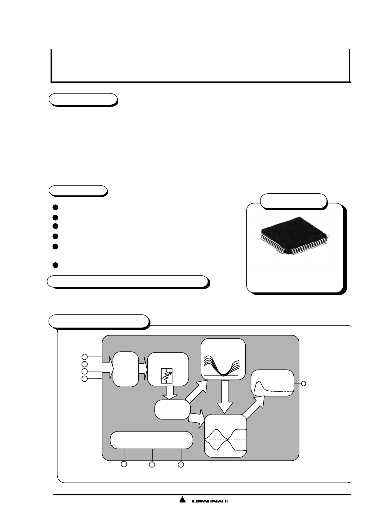
PACKAGE
Built-in 4ch input selector
Variable volume range 0 to -83dB,-∞ (1dB/step)
Built-in bass boost circuit (loudness type)
Built-in speaten filter (5 mode)
2band tone control
(0,±2.0,±4.0,±6.0,±8.0,±10.0,dB)
Bass boost 0N/OFF
RECOMMENDED OPERATING CONDITIONS
Outline 64P6N-A
0.8mm pitch QFP
(14.0mm X 14.0mm X 2.8mm)
Analog supply voltage range ------- 6.0 to 9.0V
Digital supply voltage range -------- 4.5 to 5.5V
SYSTEM CONFIGURATION
(CH1/CH2)
iN 1
IN 2
IN 3
IN 4
LATCH
Input
selector
u-com interface
DATA
volume &
Buss boost
speaten filter
ON/PASS SW
CLK
speaten filter
circuit
(CH1/CH2)
X-Bass boost
OUT
tone control
Bass treble

ELECTRONIC VOLUME CONTROL WITH BUILT-IN SPEATEN FILTER
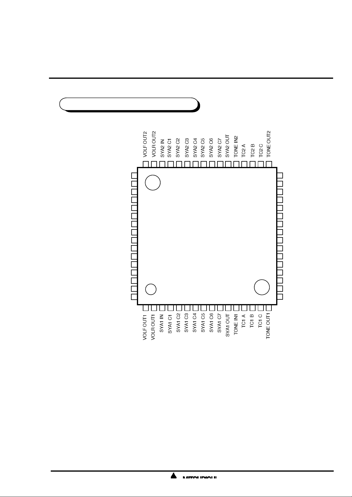
PIN CONFIGURATION(TOP VIEW)
MITSUBISHI SOUND PROCESSOR ICs
M62496FP
LOUD IN2
VOL IN2
SELECT OUT2
SELECT NF2
SELECT2 INA
SELECT2 INB
SELECT2 INC
SELECT2 IND
SELECT1 INA
SELECT1 INB
SELECT1 INC
SELECT1 IND
SELECT NF1
SELECT OUT1
VOL IN1
LOUD IN1
484647
49
50
51
52
53
54
55
56
57
58
59
60
61
62
63
64
1
2
44
45
43 42
4140393837
M62496FP
5 6 7
4
3
8 9
10 11 12
36
13
33
35
34
FBB2
32
NFBB2
31
INBB2
30
OUT2
29
SYA VREF2
28
VREF
27
VCC
26
CLOCK
25
DATA
24
VDD
23
GND
22
SYA VREF1
21
OUT1
20
INBB1
19
NFBB1
18
FBB1
17
15 16
14

ELECTRONIC VOLUME CONTROL WITH BUILT-IN SPEATEN FILTER
MITSUBISHI SOUND PROCESSOR ICs
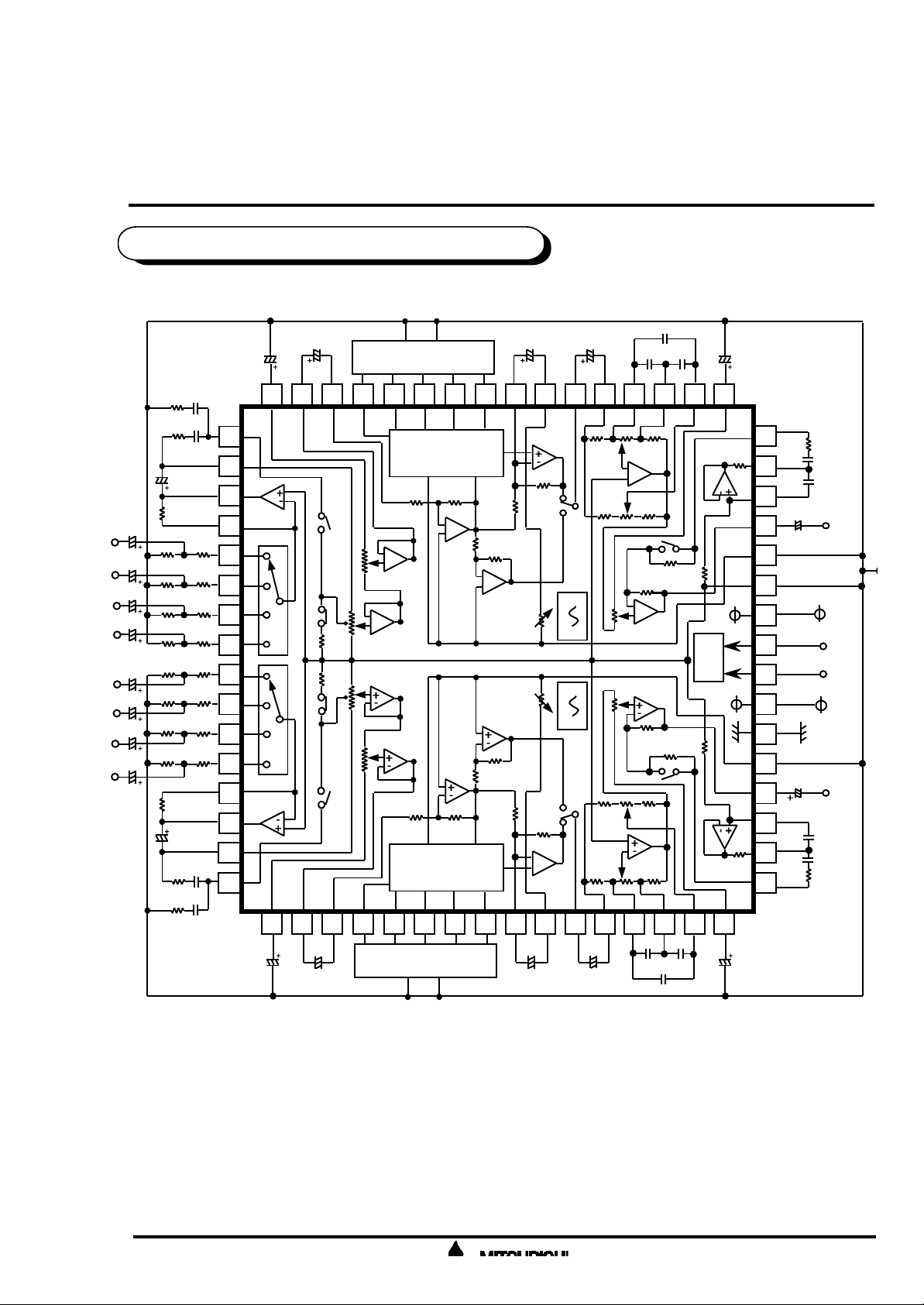
IC INTERNAL BLOCK DIAGRAM
VREF
3
2
5
0.068µ
0.068µ
+++
M62496FP
2.2µ
2.2µ
2.2µ
2.2µ
2.2µ
2.2µ
2.2µ
2.2µ
0.1µ4.7K
68K 680p
2.2µ
15K
47
47K
15K
K
47K
15K
47K
15K
47K
15K
47K
15K
47K
15K
47K
15K
47K 15K
15K
2.2µ
68K 680p
49
50
51
52
53
54
55
56
57
58
59
60
61
62
63
64
4.7µ
A
B
C
D
A
B
C
D
48 4647
2.2µ
Speaten Filter
45 44
43
Speaten Filter
+
+
Speaten Filter
42
+
40
41
+
Control of
Speaten
filter
Control of
Speaten
filter
100µ
39 38
0dB
-28dB
0dB
-28dB
+
SW5
SW5
2.2µ
37
36
+
+
10K
10K
0.0068µ
0.0068µ
35
160K
160K
34 33
56K
I/F
56K
1.5K
1.5K
4.7µ
32
31
30
29
28
27
26
25
24
23
22
21
20
19
18
17
3.3K
1µ
0.033µ
2.2µ
+
2ch OUT
CLOCK
DATA
GND
2.2µ
1ch OUT
0.033µ
1µ
3.3K
VCC
VDD
0.1µ4.7K
4.7µ
1
2.2µ
4
Speaten Filter
2.2µ
13 14
0.0068µ
0.0068µ
15 16
4.7µ
6
7
8 9
100µ
10
11 12

ELECTRONIC VOLUME CONTROL WITH BUILT-IN SPEATEN FILTER
MITSUBISHI SOUND PROCESSOR ICs
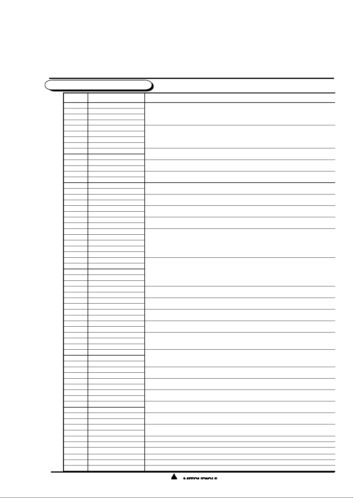
PIN DESCRIPTION
M62496FP
Pin No.
57
58
59
60
53
54
55
56
61
52
62
51
63
50
64
49
1
48
2
47
3
46
4
5
6
7
8
45
44
43
42
41
9
10
40
39
11
38
12
37
13
14
15
36
35
34
16
33
17
32
18
31
19
30
20
29
21
28
22
23
24
25
26
27
Symbol
SELECT1 IN A
SELECT1 IN B
SELECT1 IN C
SELECT1 IN D
SELECT2 IN A
SELECT2 IN B
SELECT2 IN C
SELECT2 IN D
SELECT NF1
SELECT NF2
SELECT OUT1
SELECT OUT2
VOL IN1
VOL IN2
LOUD IN1
LOUD IN2
VOLF OUT1
VOLF OUT2
VOLR OUT1
VOLR OUT2
SYA1 IN
SYA2 IN
SYA1 C1
SYA1 C2
SYA1 C3
SYA1 C4
SYA1 C5
SYA2 C1
SYA2 C2
SYA2 C3
SYA2 C4
SYA2 C5
SYA1 C6
SYA1 C7
SYA2 C6
SYA2 C7
SYA1 OUT
SYA2 OUT
TONE IN1
TONE IN2
TC1 A
TC1 B
TC1 C
TC2 A
TC2 B
TC2 C
TONE OUT1
TONE OUT2
FBB1
FBB2
NFBB1
NFBB2
INBB1
INBB2
OUT1
OUT2
SYA VREF1
SYA VREF2
GND
VDD
DATA
CLOCK
VCC
VREF
Function
Input pin for channel 1 of the input selector switch block.
Input pin for channel 2 1 of the input selector switch block.
Adjusts input gains by using the resistance between this pin and the SELECT
OUT pin and by using resistance added to INA to IND.
Output pin of the input selector switch.
Input pin of the volume block.
Pin for setting the frequency characteristics of the loudness block.
Output pin of the volume block (1st stage). Connect this pin to VREF pin with C
connection to reduce switching noise.
Output pin of the volume block (2nd stage).
Input pin of the speaten filter block.
Pin for connecting filter of the speaten filter. (ch1)
Pin for connecting filter of the speaten filter. (ch2)
Reduce switching noise on speaten filter effect by using the capacitance
between pin9 and pin10.(ch1)
Reduce switching noise on speaten filter effect by using the capacitance
between pin39 and pin410.(ch2)
Output pin of the speaten filter block.
Input pin of the tone control block.
Pin for setting frequency characteristics of the tone control block for channel 1.
Pin for setting frequency characteristics of the tone control block for channel 2.
Output pin of the tone control block.
Resonant impedance (band-pass filter) connection pin for base section.
Output pin of bass boosting resonant buffer amp.
Input pin of bass boosting resonant buffer amp.
Final output pin of the ATT block.
Ground of the speaten filter speaten filter block. Apply 1/2Vcc.
Ground pin
Digital power supply pin.
Input pin of the control data. This pin inputs data in synchronization with CLOCK.
Clock input pin for serial data transfer.
Analog power supply pin.
IC signal ground. Apply 1/2Vcc.
 Loading...