MITSUBISHI SOUND PROCESSORS
PRELIMINARY
Notice ; This is not a final specification.
some parametric limits are subject to change.
SINGLE CHIP ANALOG SOUND PROCESSOR
FEATURES
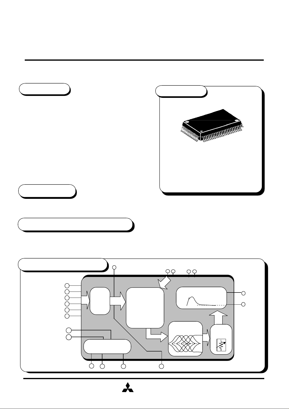
• Capable of controlling functions with serial data
6-input selector
5band tone control (0, ±3, ±6, ±10dB)
Bass boost (loudness type) [ON/OFF]
Surround (using external delay) [ON/OFF]
Voice cancel (stereo) [ON/OFF]
Multilingual record switching [L only/R only]
Electric volume 32steps ( 0dB ~ ∞ )
SW mode for control of DPL and other sound
fields 3 lines for Rec output,2 lines for port output
• Supporting digital delay
• Input/output of adapter supporting karaoke control
M62433FP
DIGITAL SOUND CONTROLLER
PACKAGE
Outline
Pitch : 0.8 mm
Size : 20.0 mm X 14.0mm
X 2.8mm
80P6N
APPLICATION
Home Audio equipment,Radio-Cassette tape recorder,TV
RECOMMENDED OPERATING CONDITIONS
Supply voltage range • • • • ±4.5 ~ ±7.3V
Rated supply voltage • • • • ±7 V
SYSTEM BLOCK DIAGRAM
IN A
IN B
IN C
IN D
IN E
IN F
PORTA
PORTB
6-Input
selector
RECOUT 2
(3-Outputs)
SW FOR:
Multilingual
switching
Vocal cancel
Surround
DPL and
other modes
KEY1 KEY2
Bass boost
Tone
OUT2
OUT1
Electric
volume
LATCH
µ -com Interface
DATA
CLK
MITSUBISHI
ELECTRIC
RECOUT1 (3-Outputs)
( / 2 1 )D - 62433Q - 78A
1
MITSUBISHI SOUND PROCESSORS
PRELIMINARY
Notice ; This is not a final specification.
some parametric limits are subject to change.
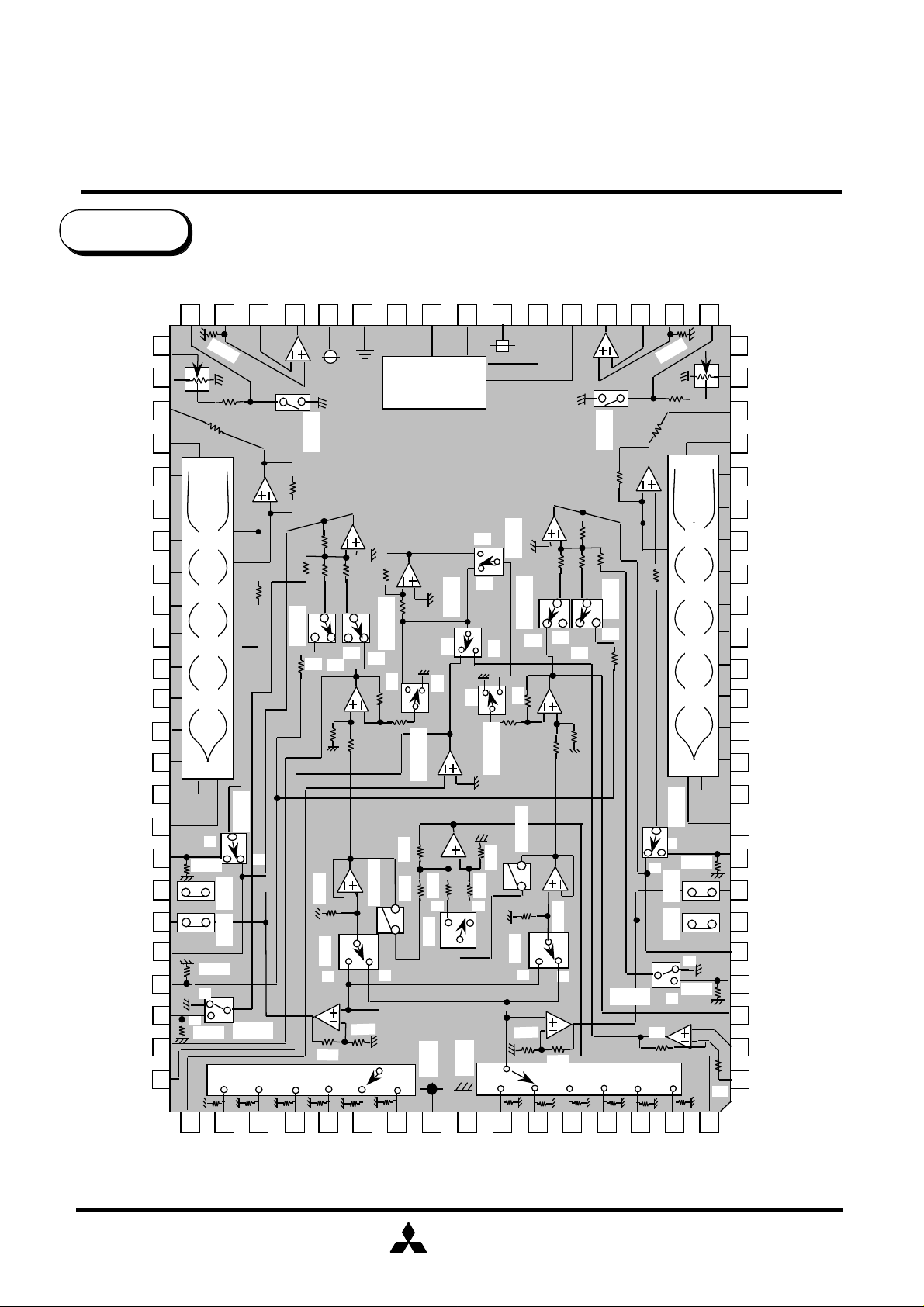
IC Internal
Block Diagram
BB2
BUFIN2
BUFNF2
BUFOUT2
40 39 38 37 36
VOLOUT2
FOUT2
F5F2
F4IN2
F4O2
F4F2
F3IN2
F3O2
F3F2
F2IN2
F2O2
F2F2
F1IN2
F1O2
F1F2
FIN2
REC2B
REC2A
REC2C
MIC IN
KEYOUT2
KEYIN2
BPFOUT
100K
41
42
43
444546
4748
49505152
SW18
5-Element Graphic Equalizer
53
54
55
56
57
58
100K
SW16
A
B
SW6SW4
59
6061
100K
B
A
626364
SW22 5K
100K
F
E
D
AVDD
SW20
A
B
100K
SW8
B
20K
C
DGND
35 34
G=2.4î{
A
B
SW12-1
8.5K
B
LATCH
33 32 31
µ -COM
SW10-2
A
SW12-2
20K
20K
A
A
DATA
interface
Logic
SW13
B
B
20K
A
SW9
SW2
CLOCK
A
B
A
B
SW11-2
20K
20K
B
SW1
A
DVDD
30
SW14
SW10-1
B
A
SW11-1
SW7
A
8.5K
B
M62433FP
DIGITAL SOUND CONTROLLER
PORTA
PORTB
BUFOUT1
29 28 27 26 25
SW19
G=2.4î{
SW17
A
100K
B
20K
C
A
B
SW21
E
D
BUFIN1
BUFNF1
100K
SW15
A
100K
B
SW5SW3
B
100K
A
F
BB1
VOLOUT1
VOLIN1VOLIN2
23 24
22
21
16 17 18 19 20
15
14
5-Element Graphic Equalizer
12 13
11
9 10
8
7
6
5
4
3
2
1
5K
FOUT11
F5F1
F4IN1
F4O1
F4F1
F3IN1
F3O1
F3F1
F2IN1
F2O1
F2F1
F1IN1
F1O1
F1F1
FIN1
REC1B
REC1A
REC1C
KEYOUT1
KEYIN1
P/S C
DELAY OUT
65 66 67 68 69 70 71 72 73 74
IN2F
BPFIN
IN2E
IN2D
IN2C
IN2B
IN2A
AVSS
AGND
MITSUBISHI
ELECTRIC
75 76
IN1A
IN1B
77
IN1C
78
IN1D
79 80
IN1E
IN1F
DELAYIN
( / 2 1 )D - 62433Q - 78A
2
MITSUBISHI SOUND PROCESSORS
PRELIMINARY
Notice ; This is not a final specification.
some parametric limits are subject to change.
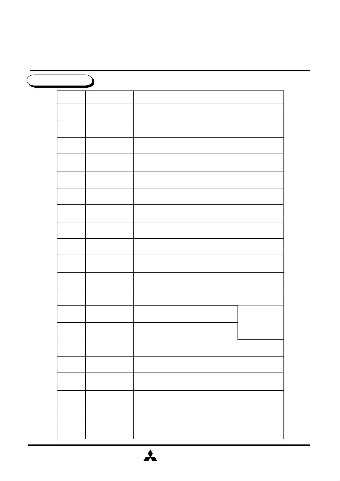
Pin Description
Pin No. Symbol Function
72
73
74,75,76
77,78,79
71,70,69
68,67,66
80
1
AVSS
AGND
IN1A,IN1B,IN1C
IN1D,IN1E,IN1F
IN2A,IN2B,IN2C
IN2D,IN2E,IN2F
DELAYIN
DELAYOUT
Negative power supply to internal analog circuit
Input pin at the side of channel1
Input pin at the side of channel2
M62433FP
DIGITAL SOUND CONTROLLER
GND of internal analog circuit
(R-L) output pin for surround. Connected to the input
of delay circuit. Total load resistance is 20kΩ
(R-L) input pin for surround.
Connected to the output of delay circuit.
2
3,63
4,62
64
65
5,60
6,59
7,58
8,57
9,46
10,45
P/S C
KEYIN1
KEYIN2
KEYOUT1
KEYOUT2
BPFOUT
BPFIN
REC1A
REC2A
REC1B
REC2B
REC1C
REC2C
FIN1
FIN2
F1F1
F1F2
F1O1
F1O2
Phase shift filter pin for surround
Key control adapter output pin. Connected to the input
of key control circuit etc. Total load resistance is 20kΩ
Key control adapter input pin.
Connected to the outputof key control circuit
Band-pass filter amplifier output pin for voice cancel
Band-pass filter amplifier input pin for voice cancel
Rec output pin A
Rec output pin B (with mute SW)
Rec output pin C (with mute SW)
Tone input pin (Surround adapter OUT)
Pin for connecting resonance impedance (band filter)
of the 1st element
Output pin of resonance buffer amplifier of the 1st element
total load
resistance ;
min. 20KΩ
11,54
12,53
13,52
F1IN1
F1IN2
F2F1
F2F2
F2O1
F2O2
Input pin of resonance buffer amplifier of the 1st element
Pin for connecting resonance impedance (band filter)
of the 2nd element
Output of resonance buffer amplifier of the 2nd element
MITSUBISHI
ELECTRIC
( / 2 1 )D - 62433Q - 78A
3
MITSUBISHI SOUND PROCESSORS
PRELIMINARY
Notice ; This is not a final specification.
some parametric limits are subject to change.
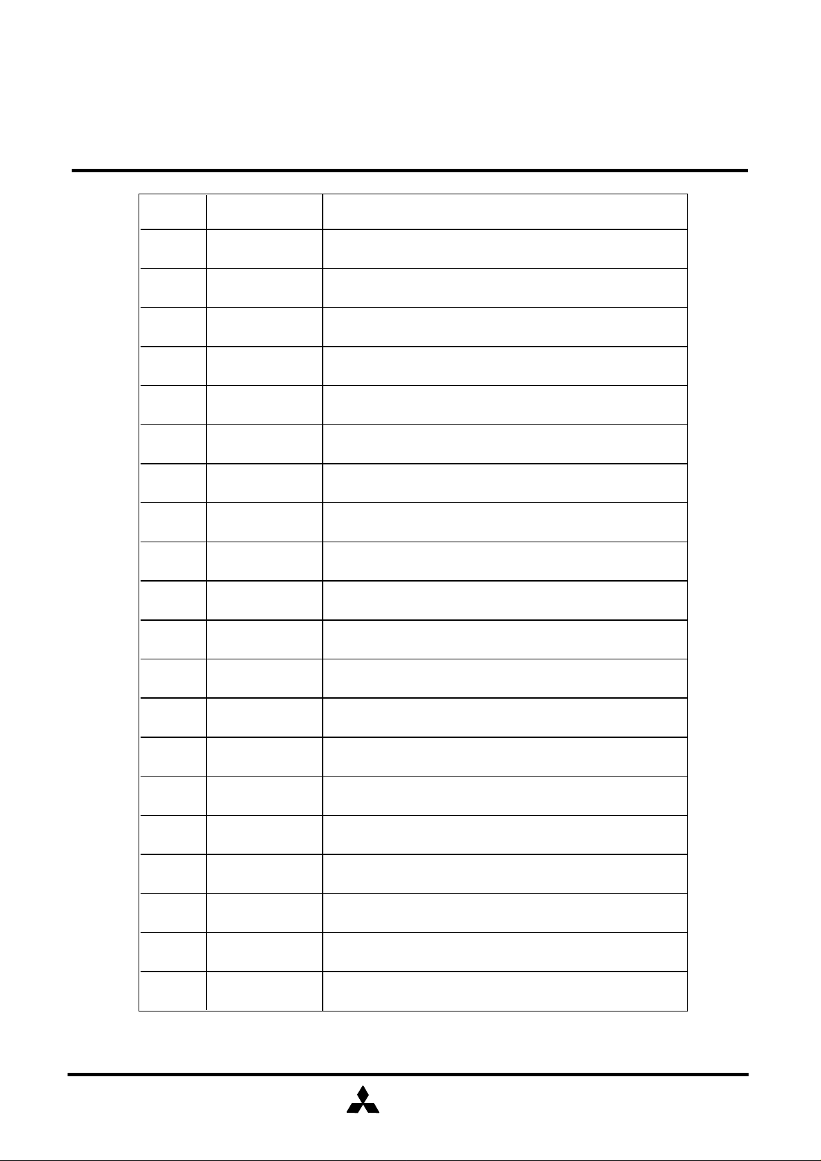
Pin No. Symbol Function
14,51
15,50
16,49
17,48
18,47
19,46
20,45
21,44
22,43
23,42
24,41
25,40
26,39
27,38
28,37
F2IN1
F2IN2
F3F1
F3F2
F3O1
F3O2
F3IN1
F3IN2
F4F1
F4F2
F4O1
F4O2
F4IN1
F4IN2
F5F1
F5F2
FOUT1
FOUT2
VOLIN1
VOLIN2
VOLOUT1
VOLOUT2
BB11
BB12
BUFIN1
BUFIN2
BUFNF1
BUFNF2
BUFOUT1
BUFOUT2
Input pin of resonance buffer amplifier of the 2nd element
Pin for connecting resonance impedance (band filter)
of the 3rd element
Output pin of resonance buffer amplifier of the 3rd element
Input pin of resonance buffer amplifier of the 3rd element
Pin for connecting resonance impedance (band filter)
of the 4th element
Output pin of resonance buffer amplifier of the 4th element
Input pin of resonance buffer amplifier of the 4th element
Pin for connecting band filter of the 5th element
Tone output pin. Capacitor is combined for connection
with the next stage.
R-ladder volume input pin
R-ladder volume output pin
Bass boost capacitance connection pin.
Sets frequency characteristics.
+input pin of bass boost output amplifier
-input pin of bass boost output amplifier
Output pin of bass boost output amplifier
M62433FP
DIGITAL SOUND CONTROLLER
29
30
31
32
33
PORTA
PORTB
DVDD
CLOCK
DATA
Output of port A
Output of port B
Power supply to internal logic circuit
Clock input pin for serial data transfer
Input pin of control data.
Reads data at the rising edge of clock.
MITSUBISHI
ELECTRIC
( / 2 1 )D - 62433Q - 78A
4
MITSUBISHI SOUND PROCESSORS
PRELIMINARY
Notice ; This is not a final specification.
some parametric limits are subject to change.
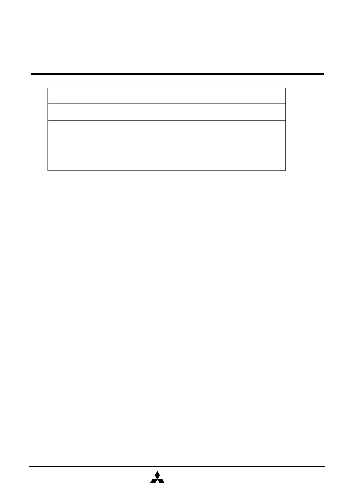
Pin No. Symbol Function
34
35
36
LATCH
DGND
AVDD
61 MIC IN
Input pin of latch signal. The circuit status changes
at the rising edge of latch signal.
GND pin of internal logic circuits
Positive power supply pin of internal analog circuits
Microphone input pin
M62433FP
DIGITAL SOUND CONTROLLER
MITSUBISHI
ELECTRIC
( / 2 1 )D - 62433Q - 78A 5
MITSUBISHI SOUND PROCESSORS
PRELIMINARY
Notice ; This is not a final specification.
some parametric limits are subject to change.
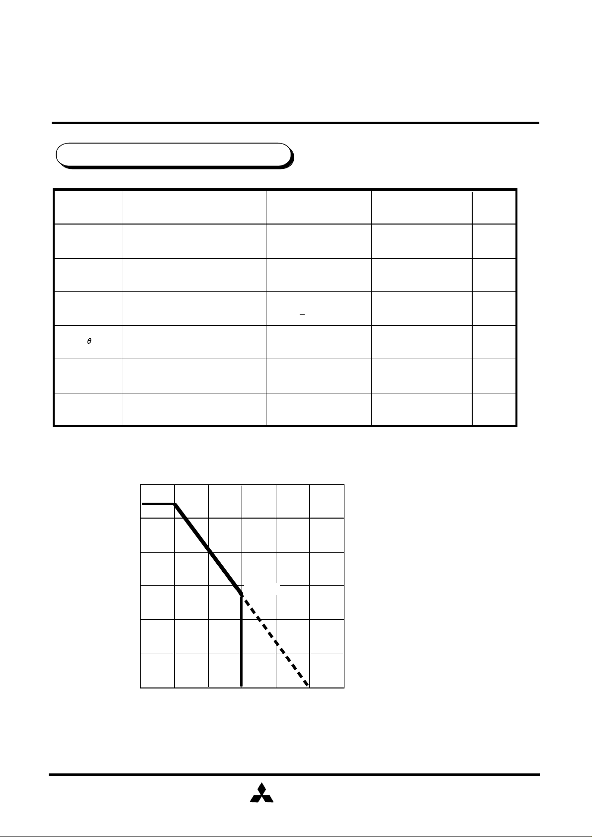
ABSOLUTE MAXIMUM RATINGS
Symbol
DVDD
Pd
K
Parameter Conditions Ratings Unit
Analog Power supplyAVDD,AVSS
Digital Power supply
Power dissipation
Thermal derating
Ta ≤ 25°C
Ta > 25°C
Attached PC Board*
M62433FP
DIGITAL SOUND CONTROLLER
±7.5
6.0
1370
13.7
V
V
mW
mW/°C
Topr
Tstg
Operating temperature
Storage temperature
Thermal derating
(Maximum ratings)
1.5
1.37W
1.0
0.5
Power dissipation pd [W]
685mW
-20 ~ +75
-55 ~ +125
*Note : PC Board
PC Board Size
140 mm X140 mm
PC Board Thickness
1.6 mm
PC Board Material
Epoxy
Copper Film Thickness
18 µm
Copper Foil Size
0.25 mm X 50 mm
°C
°C
0
0
25 50 75 100
Ambient Temperature Ta [°C ]
125
MITSUBISHI
ELECTRIC
150
( / 2 1 )D - 62433Q - 78A
6
MITSUBISHI SOUND PROCESSORS
PRELIMINARY
Notice ; This is not a final specification.
some parametric limits are subject to change.
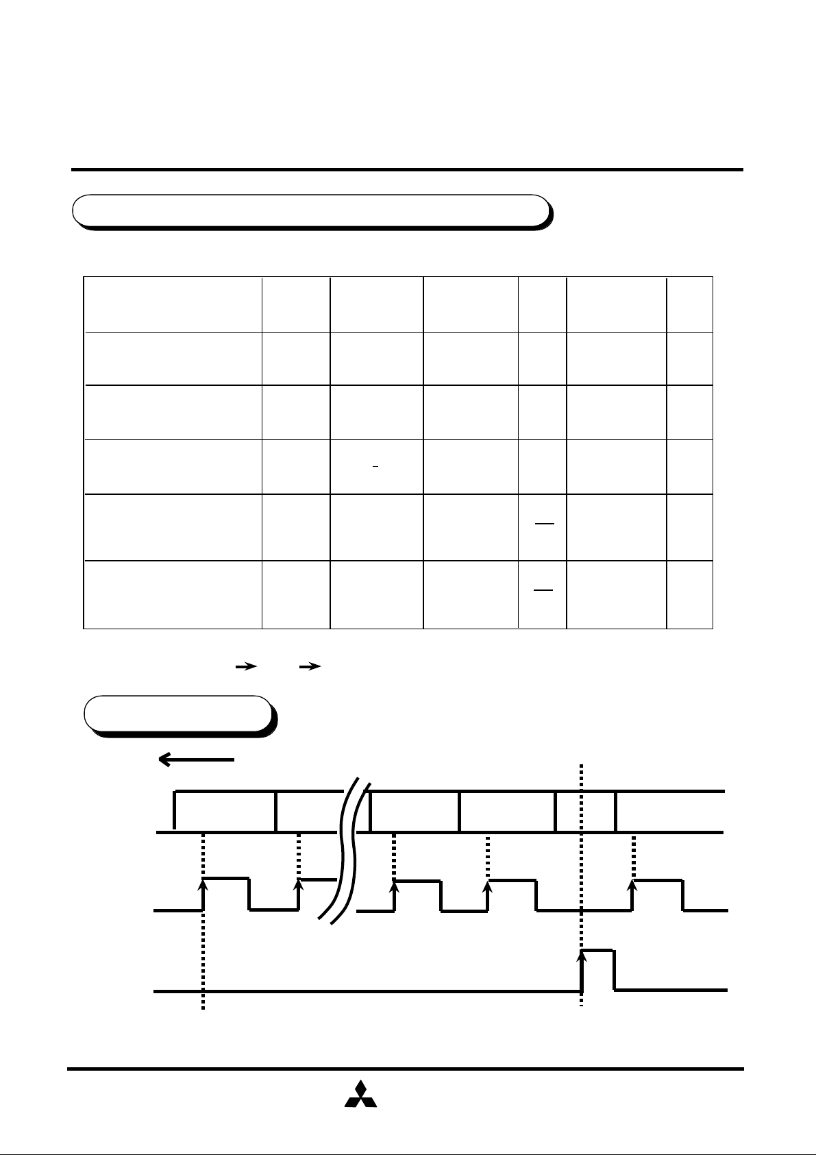
RECOMMENDED OPERATING CONDITIONS
( Ta=25°C, unless otherwise noted )
Analog (+) power supply
Analog (-) power supply
Digital power supply
SymbolParameter Conditions
AVDD
AVSS
DVDD
Note 1
Note 1
DVDD≤AVDD
MIN
4.5
-4.5 -7.0 -7.3
4.5
M62433FP
DIGITAL SOUND CONTROLLER
TYP
7.0
MAX
7.3
5.0 5.5
Unit
V
V
V
Logic
” H ” Level
VIH
input voltage
Logic
” L ” Level
VIL
input voltage
Note 1: The sequence of the power supply is as follows.
AVDD AVSS DVDD
TIMING DIAGRAM
H
DATA
CLOCK
D0
L
H
L
D1
VDDDVDD-0.7
0
DGND+0.7
V
V
Latch Signal
D7D6
D0
LATECH
H
L
DATA reading mode;
The rising edge of the CLOCK signal
MITSUBISHI
ELECTRIC
LATCH reading mode;
The rising edge of the LATCH signal
( / 2 1 )D - 62433Q - 78A
7
 Loading...