MITSUBISHI (Dig./Ana. INTERFACE)
LATCH
CONVERTER
LATCH
CONVERTER
LATCH
CONVERTER
LATCH
CONVERTER
8-BIT LATCH
12-BIT LATCH
OUTPUT DATA 4-BIT LATCH
CIRCUIT
M62376GP
8-BIT 12CH D-A CONVERTER IC BUILT-IN 12-BIT I/O EXPANDER
DESCRIPTION
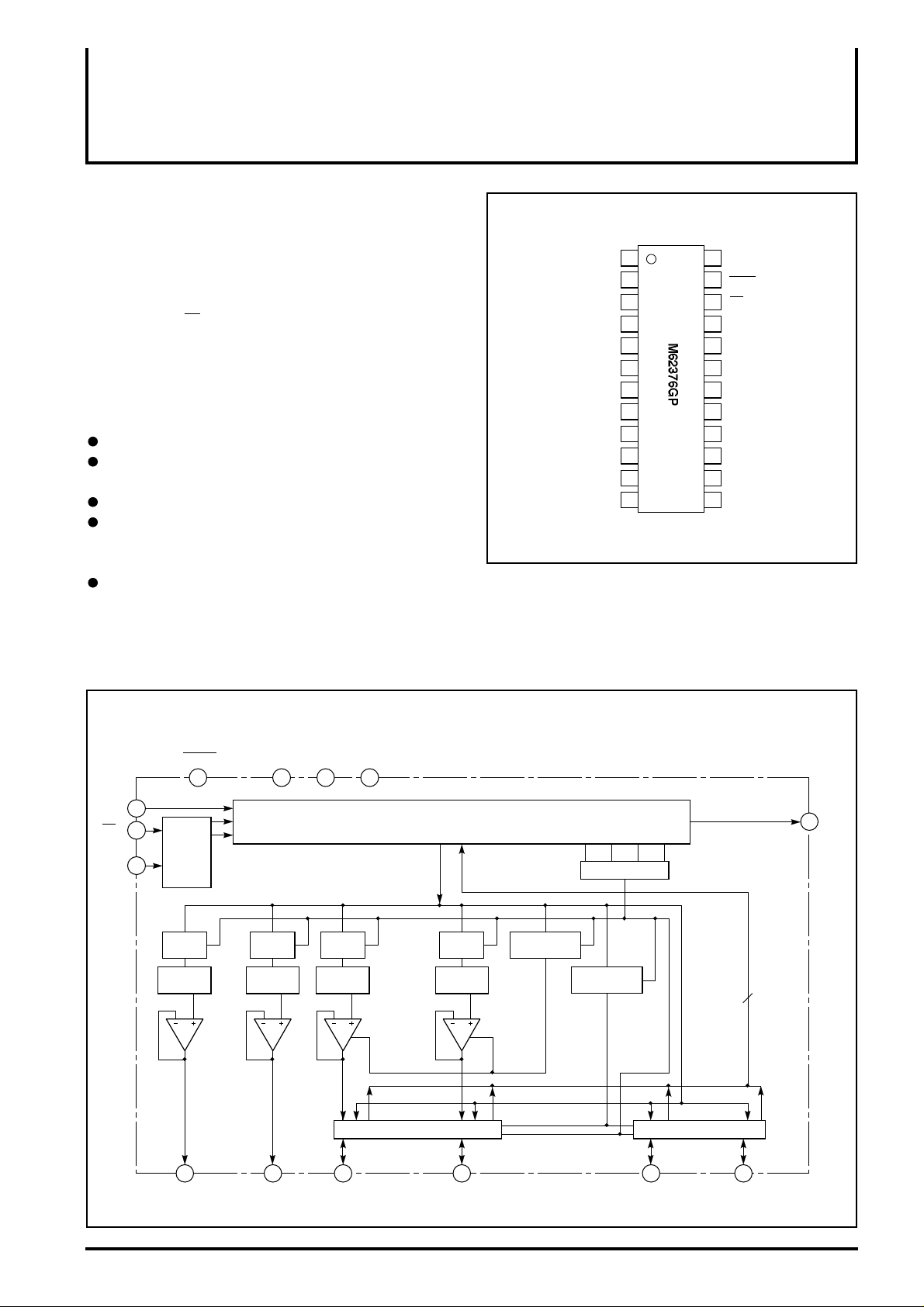
The M62376GP is a semiconductor IC that adopts a CMOS
structure having 12-channel of 8-bit D-A converter and 12-bit I/O
expander. The IC has achieved a wide operation range of 2.7V to
5.5V in power voltage.
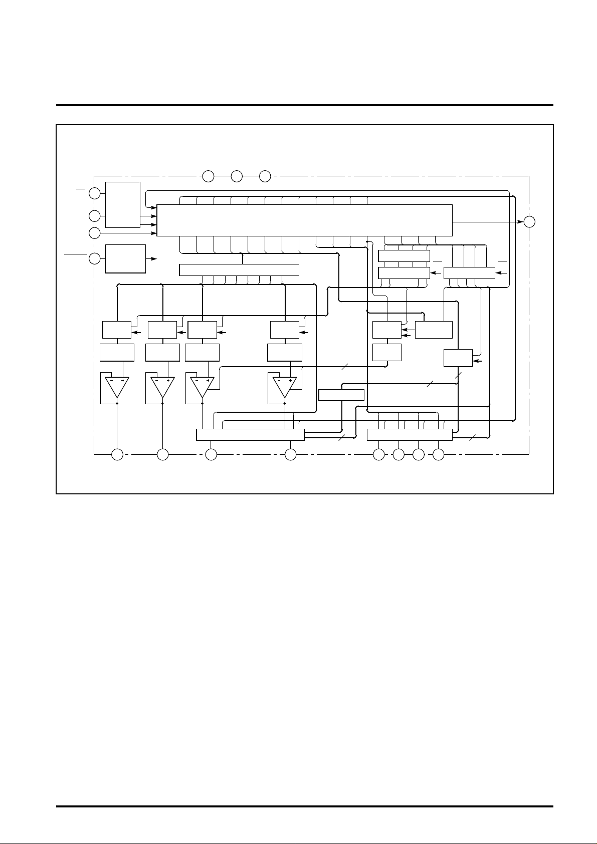
Data is easily available via 3-wire combination system serial input
of SI, CLK and EN. The IC also provides an SO pin enabling
cascade connection. It provides 8 pins that share D-A converter
and I/O ports that can be arbitrarily switched with serial
input data.
FEATURES
Supply voltage 2.7 to 5.5V
Adopts 4 special ports for each of DAC and I/O and 8 ports that
share DAC output and I/O.
Each port can be set by serial data for input/output status.
Built-in power-on reset where D-A output is set to "L" in the
initial status and I/O goes to Hi-impedance when power is
turned on.
Small package of 0.65mm pitch and 24 pin.
PIN CONFIGURATION (TOP VIEW)
A1
1
2
A2
A3
3
A4 SO
4
D11/A5 SI
D10/A6 CLK
D6/A10
D5/A11 VCC
D4/A12 VDD
5
D9/A7 D0
D8/A8 D1
8
D7/A9 D2
Outline 24P2E-A
GND
24
23
REST
22
EN
21
20
196
187
17
169
D3
1510
1411
1312
APPLICATION
Adjustment/control of industrial or home-use electronic equipment,
such as VCR camera, VCR set, TV, and CRT display.
BLOCK DIAGRAM
RESET
23 13 14 24
20
SI
22
EN
CLK
CLOCK
CONTROL
19
8-BIT
8-BIT D-A
VCC
VDD
S15 S14 S13 S12 S11 S10 S9 S8 S7 S6 S5 S4
•••
8-BIT
8-BIT D-A
•••
•••
GND
SHIFT REGISTER
8-BIT
8-BIT D-A
••••••
••••••
••••••
••••••
••••••
OUTPUT DATA 8-BIT LATCH
8-BIT
8-BIT D-A
A12A5A4A1
Amp. Hi-Z
S3 S2 S1 S0
DECODER
I/O SELECT
(12)
21
SO
A1
1
4
••• D11/A5 •••••• D4/A12 D3 D0
A4
12 15 185
••••••

EXPLANATION OF TERMINALS
Pin No. FunctionSymbol
20
21
19
22
1
2
3
4
5
6
7
8
9
10
11
12
18
17
16
15
14
24
13
23
SI
SO
CLK
EN
A1
A2
A3
A4
D11/A5
D10/A6
D9/A7
D8/A8
D7/A9
D6/A10
D5/A11
D4/A12
D0
D1
D2
D3
VCC
GND
VDD
RESET
Serial data input pin. Enters serial data of 16-bit in length.
Outputs data from 16-bit shift register that reads serial data or parallel data.
Shift clock input pin. At the rise of shift clock, input signal from the SI pin is entered into the 16-bit
shift register.
Entry of low level into the EN pin starts to read data.
Putting 16-bit data at high level after input loads the input data to a specified register.
Special output pin for 8-bit D-A converter (DAC)
Pin that shares I/O and DAC output.
Settings can be selected with serial data.
D4 to D11 are connected to the VDD power supply.
Digital input output pin.
Digital block power supply pin.
GND pin
Power supply pin in analog block and reference voltage input pin on the upper side of D-A converter
RESET pin
MITSUBISHI (Dig./Ana. INTERFACE)
M62376GP
8-BIT 12CH D-A CONVERTER IC BUILT-IN 12-BIT I/O EXPANDER

8-BIT 12CH D-A CONVERTER IC BUILT-IN 12-BIT I/O EXPANDER
CONTROL
RESET
DECODER (12)
DECODER (4)
LATCH
LATCH
LEVEL SHIFT
(A5 to A12 Hi-Z)
LATCH
CONVERTER
LATCH
CONVERTER
LATCH
CONVERTER
LATCH
CONVERTER
EXPLANATION OF TERMINALS BLOCK DIAGRAM
VDD VCC GND
13 14 24
EN
22
CLK
CLOCK
19
20
SI
Di11 Di10 Di9 Di8 Di7 Di6 Di5 Di4 Di3 Di2 Di1 Di0
EN
CLK
S15 S14 S13 S12 S11 S10 S9 S8 S7 S6 S5 S4 S3 S2 S1 S0
SHIFT REGISTER
MITSUBISHI (Dig./Ana. INTERFACE)
M62376GP
[1110]
21
SO
RESET
POWER ON
23
8-BIT
8-BIT D-A
8-BIT
•••
8-BIT D-A
•••
•••
1 12 15 16 17 184 5
•••
A1 A4
8-BIT
8-BIT D-A
D11/A5
LEVEL SHIFT
••••••
••••••
••••••
LATCH
••••••
LEVEL SHIFT
•••••
8-BIT
8-BIT D-A
(8)
8-BIT
LEVEL
SHIFT
[11010000]
(8)
A12A5A4A1
LATCH
(8)
D4/A12 D3 D2 D1 D0
ENEN
[0000]
[1111]
12-BIT
(12)
[1101]
(4)
 Loading...