MITSUBISHI<Dig.Ana.INTERFACE>
control in combination with a microcomputer.
resistor)
-
LATCH X 4
D15 D14 D13 D12 D11 D10 D9 D8
D5 D4 D3 D2 D1 D0
M62370GP
3V TYPE 8-BIT 36CH SELECTOR SW BUILT-IN D-A CONVERTER WITH BUFFER AMPLIFIERS
DESCRIPTION
The M62370GP is a CMOS semiconductor IC,containing 36
channels of 8-bit D-A converters.It is operable with a low
supply voltage between 2.7~3.6V,and is easy to use due to
serial data input,and 3-pin(DI,CLK,LD)connection with
microcomputer.The IC also contains Do pin terminal,enabling
cascade connection,and therefore is suitable for automatic
FEATURES
•Operable with a low voltage between 2.7~3.6V
•16-bit serial data input(connected via 3 pins:DI,CLK,LD)
•36 channels built-in of 8-bit D-A converter
•6 channels of D-A converters capable of selecting and
outputting 4 data stored in each converter,through
2 control terminals
APPLICATION
Digital-analog conversion in industrial or home-use
electronic equipment.
Automatic control in combination with EEPROM and
microcomputer(Substitute for conventional semi-fixed
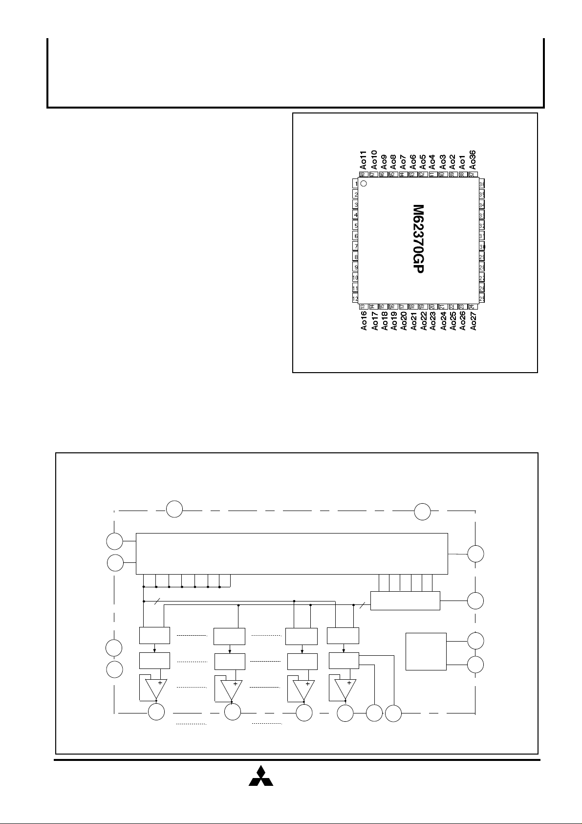
PIN CONFIGURATION (TOP VIEW)
DI
CLK
LD
Do
GND
C0
Vss1
VDD1
Ao12
Ao13
Ao14
Ao15
Outline 48P6D-A
Ao35
Ao34
Ao33
Ao32
Vss2
VDD2
C1
Vcc
Ao31
Ao30
Ao29
Ao28
BLOCK DIAGRAM
CLK
2
DI
1
8-BIT
VDD1
Vss1
8
7
LATCH
D-A
-
38 21
Ao1
8
VCC
29
16-BIT SHIFT REGISTER
8-BIT
D-A
Ao24 Ao35 Ao36
8-BIT
LATCH X 4
D-A
-
36 37
8-BIT
LATCH X 4
D-A
-
DECODER
31
VDD232Vss2
GND
5
DATA
CONTROL
30
Do
4
LD
3
Co
6
C1
MITSUBISHI
ELECTRIC
( / 5 )
1

3V TYPE 8-BIT 36CH SELECTOR SW BUILT-IN D-A CONVERTER WITH BUFFER AMPLIFIERS
EXPLANATION OF TERMINALS
Pin No. Symbol
1
4
2
3
38
DI
Do
CLK
LD
Ao1
MITSUBISHI<Dig.Ana.INTERFACE>
M62370GP
Function
Serial data input terminal to input 16-bit long ssrial data
Terminal to output MSB data of 16-bit shift register
Shift clock input terminal.Input signal at DI pin is input to 16-bit shift register at rise of shift clock pulse
When H-level signal is input to this terminal,the value stored in 16-bit shift register is loaded
in decoder and D-A converter output register
48
9
28
33
37
29
5
6
30
8
7
31
32
Ao11
Ao12
Ao31
Ao32
Ao36
VCC
GND
C0
C1
VDD1
VSS1
VDD2
VSS2
8-bit D-A converter output terminal
Power supply terminal
GND terminal
Data sslect signal input terminal 1 for channel No.31 through 36
Data select signal input terminal 2 for channel No.31 through 36
Upper reference voltage input terminal and power supply to operational amplifier for channel No.1 through 24
Lower reference voltage input terminal for channel No.1 through 24
Upper reference voltage input terminal and power supply to operational amplifier for channel No.25 through 36
Lower reference voltage input terminal for channel No.25 through 36
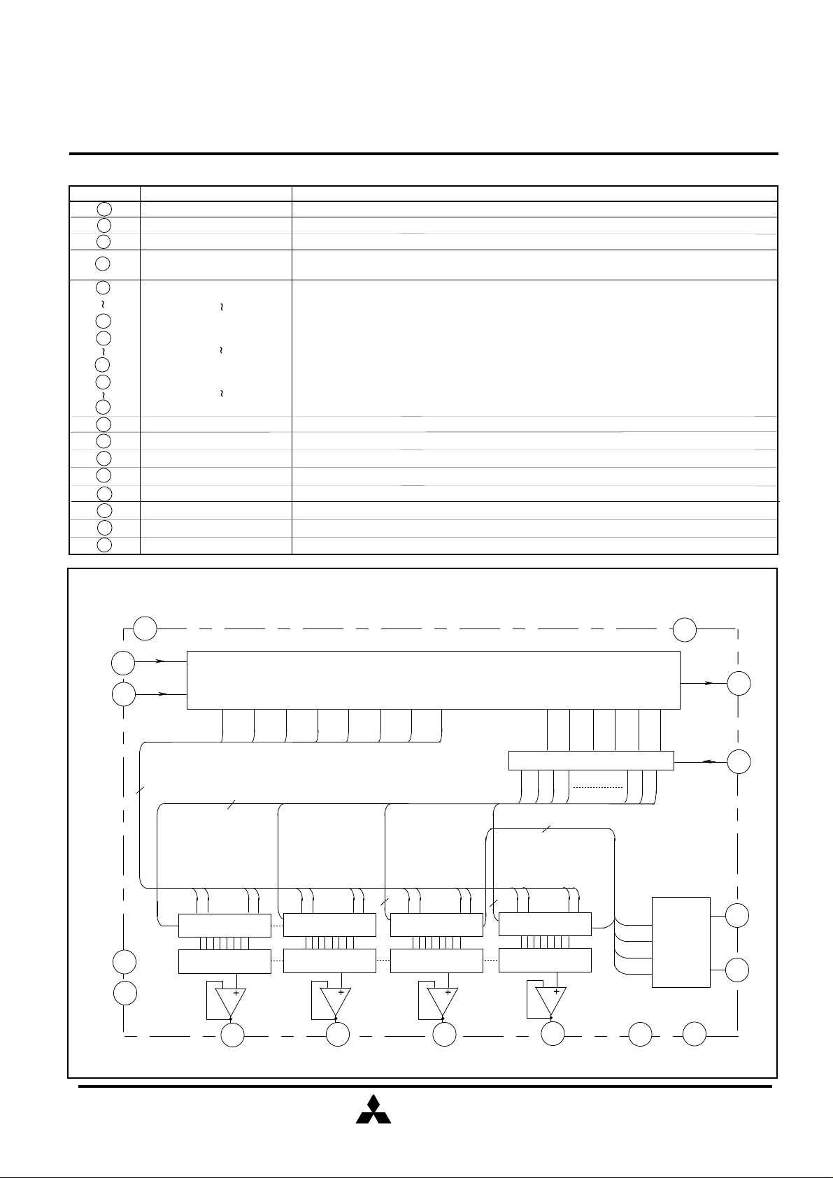
BLOCK DIAGRAM FOR EXPLANATION OF TERMINALS
Vcc
29
2
CLK
1DI
D15
D14
D13
D12
16-BIT SHIFT REGISTER
D11
D10
D9 D8
D7
D6
D5
D4
D3 D2
GND
5
43Do
D1 D0
VDD1
ADDRESS DECODER
(8)
............
8-BIT
LATCH
1
8
7Vss1
8-BIT
D-A CONVERTER
-
38
Ao1
............
8-BIT
LATCH
DAC
-
27
Ao30
(4)
............
8-BIT LATCH X 4
3130
DAC
SEL
-
28
Ao31
36
MITSUBISHI
ELECTRIC
3
21
4
(4)
............
(4)
8-BIT LATCH X 4
SEL
8-BIT
D-A CONVERTER
-
37
Ao36
CONTROL
31
VDD2
DATA
32
Vss2
( / 5 )
2
LD
630C0
C1
 Loading...