MITSUBISHI<Dig.Ana.INTERFACE>
to use due to serial data input,and 3-pin(DI,CLK,LD)connection with
microcomputer.
The IC also contains Do pin terminal,enabling cascade
connection.The built-in buffer operational amplifiers are of full-swing
design with a wide operating supply voltage range for input/output
voltage.In addition,this IC provides improved stability against a
capacitive load,and therefore is suitable for application to electronic
volume(VCA)control,substitute for adjustment semi-fixed
resistor,etc.
operational amplifiers.
display.
D0D7123456D8
9
10
-
-
M62366GP
3V TYPE 8-BIT 12CH D-A CONVERTER WITH BUFFER AMPLIFIERS
DESCRIPTION
The M62366GP is a CMOS semiconductor IC,containing 12
channels of 8-bit D-A converters,with a high-performance buffer
operational amplifier provided in the output of each channel. It is
operable with a low supply voltage between 2.7~3.6V,and is easy
FEATURES
•Operable with a low voltage between 2.7~3.6V
•12-bit serial data input(connected via 3 pins:DI,CLK,LD)
•12 channels of R-2R and segment type high-performance 8-bit
D-A converters
•12 buffer operational amplifiers with full swing of output voltage
between Vcc and GND.
•High oscillation stability against the capacitive load of buffer
APPLICATION
Adjustment/control of industrial or home-use electric
equipment,such as VTR camera,VTR set,TV,and CRT
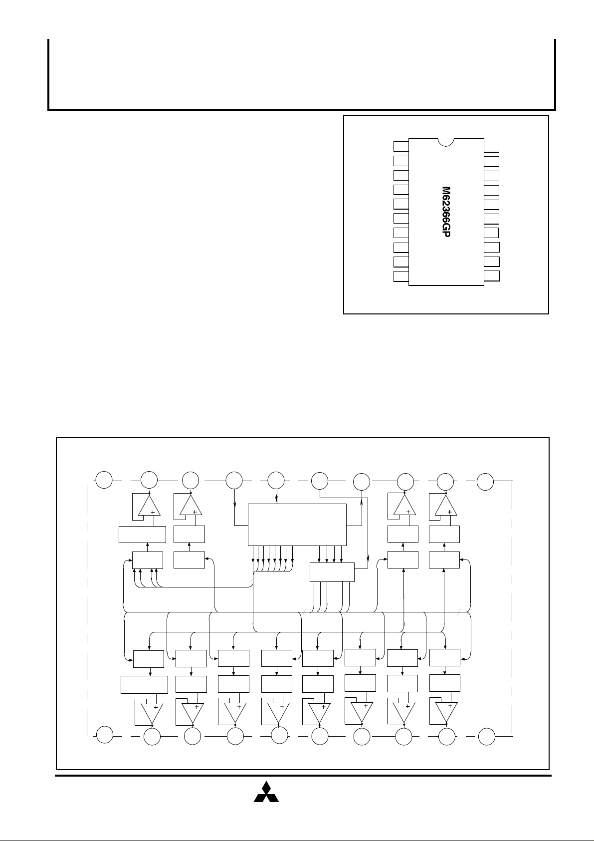
PIN CONFIGURATION (TOP VIEW)
VSS
(VrefL)
Ao3
Ao4
Ao5
Ao6
Ao7
Ao8
Ao9
Ao10
VDD
(VrefU)
1
2
3
4
5
6
7
8
9
10
Outline 20P2E-A
20
GND
19
Ao2
18
Ao1
DI
17
16
CLK
15
LD
14
Do
Ao12
13
12
Ao11
Vcc
11
BLOCK DIAGRAM
GND
20 19
BUFFER
OPERATIONAL
AMPLIFIER
1
Vss
(VrefL)
Ao2
-
8-BIT
R-2R + SEGMENT
D-A CONVERTER
Ch2
8-BIT
LATCH
.....
(12)
8-BIT
LATCH
Ch3
8-BIT
R-2R + SEGMENT
D-A CONVERTER
-
2
Ao3
Ao1
DI
18 17 16
12-BIT SHIFT REGISTER
D-A
1
L
L
4
D-A
-
L
5
D-A
-
3 4
Ao4
Ao5
(8)
CLK
LD Do
15
D11
ADDRESS
DECODER
7
.....
L
8
D-A
(12)
L
6
D-A
-
5
6
Ao6 Ao7 Ao8
MITSUBISHI
ELECTRIC
Ao12 Ao11 Vcc
14 13 12
D-A
12 11
L
L
D-A
-
9
L
10
D-A
-
7 8 9
Ao9
-
D-A
L
L
D-A
-
Ao10
(12)
11
10
VDD
(VrefU)
( / 5 )
1

3V TYPE 8-BIT 12CH D-A CONVERTER WITH BUFFER AMPLIFIERS
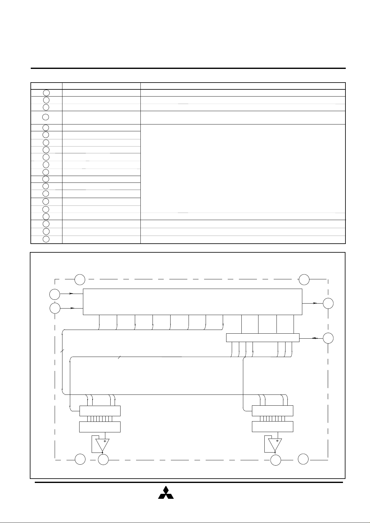
EXPLANATION OF TERMINALS
Pin No. Symbol
17
14
16
15
18
19
2
3
4
5
6
7
8
9
12
13
11
20
10
1
DI
Do
CLK
LD
Ao1
Ao2
Ao3
Ao4
Ao5
Ao6
Ao7
Ao8
Ao9
Ao10
Ao11
Ao12
VCC
GND
VDD
VSS
MITSUBISHI<Dig.Ana.INTERFACE>
M62366GP
Function
Serial data input terminal to input 12-bit long serial data
Terminal to output MSB data of 12-bit shift register
Shift clock input terminal.Input signal at DI pin is input to 12-bit shift register at rise of shift clock pulse
When H-level signal is input to this terminal,the value stored in 12-bit shift register is loaded
in decoder and D-A converter output register
8-bit D-A converter output terminal
Power supply terminal
GND terminal
D-A converter upper reference voltage input terminal
D-A converter lower reference voltage input terminal
BLOCK DIAGRAM FOR EXPLANATION OF TERMINALS
Vcc
11
DI
17
12-BIT SHIFT REGISTER
16
CLK
8
1
D0
8-BIT
R-2R + SEGMENT
D-A CONVERTER
D0
............
8-BIT
LATCH
-
D1
D2
12
D7
..............................................12
..............................................
...................................................................................................
D3
D4
D5
D6 D7
D8
D9
D10 D11
ADDRESS DECODER
...............
3
21
............
D0
8-BIT
LATCH
8-BIT
R-2R + SEGMENT
D-A CONVERTER
-
GND
20
1415Do
LD
124
D7
10
VDD
(VrefU)
18
Ao1
MITSUBISHI
ELECTRIC
13
Ao12
1
Vss
(VrefL)
( / 5 )
2
 Loading...