MITSUBISHI<Dig.Ana.INTERFACE>
range is able to change severally make use of gain set up data.
Signal gain control of DISPLAY-MONITOR or CTV.
R-2R D-A
G
G
GGG
G
M62359P,FP
8-BIT 8CH D-A CONVERTER WITH BUFFER AMPLIFIERS
DESCRIPTION
The M62359 is a 8-channel 8-bit voltage output digital to analog
converter.
The M62359 includes data latch circuit and gain change circuit of
output amplifiers.
Input data is a easy-to-use three-wires serial interface.
It is able to cascading serial use with Do terminal.
Gain set up data change a case the each channel`s output
voltage range is change ,and each channel`s output voltage
FEATURES
•All channel includes gain change latch circuit with output
amplifiers.
•14-bit serial data input
•Built-in reset circuit
APPLICATION
Conversion from digital control data to analog control data
for home-use and industrial equipment.
Automatic adjustment by combination with EEPROM and
microcomputer(replacement of conventional half-fixed
resistor).
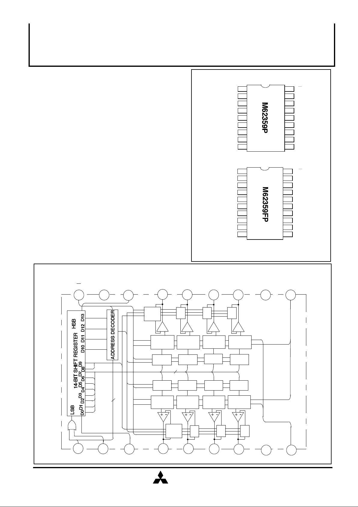
PIN CONFIGURATION (TOP VIEW)
R
LD
CLK
Ao5
Ao6
Ao7
Ao8
GND
VrefL
LD
CLK
DI
Ao5
Ao6
Ao7
Ao8
NC
GND
VrefL
1
2
DI
3
4
Outline 18P4
1
2
3
4
Outline 20P2N-A
18
VDD
17
DO
16
15
145
136
Ao2
127
118
109
20
19
18
17
Ao4
165
Ao3
156
Ao2
147
Ao1
138
NC
129
Vcc
1110
VrefU
Ao4
Ao3
Ao1
Vcc
VrefU
R
VDD
DO
BLOCK DIAGRAM
R
VDD
NC:NO CONNECTION
GAIN
CHANGE
LATCH
R-2R D-A
LATCH
LATCH
Ao4
-
8-BIT
8-BIT
8-BIT
8-BIT
+
Do
2
8
GAIN
CHANGE
LATCH
Ao3
+
-
L
R-2R R-2R
Ao2
-
R-2RR-2R
LL
Ao1
+
-
R-2R
LL
L
R-2R
+
Vcc
VrefU
LD
CLK
DI
Ao5
MITSUBISHI
ELECTRIC
Ao6
Ao7
Ao8
GND
VrefL
( / 6 )
1

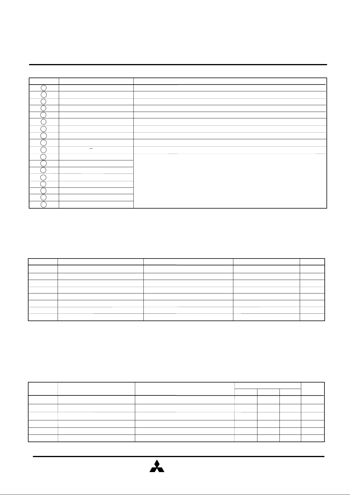
EXPLANATION OF TERMINALS
Pin No. Symbol
3
16
2
1
17
11
8
10
9
18
12
13
14
15
4
5
6
7
DI
DO
CLK
LD
VDD
Vcc
GND
VrefU
VrefL
R
Ao1
Ao2
Ao3
Ao4
Ao5
Ao6
Ao7
Ao8
MITSUBISHI<Dig.Ana.INTERFACE>
M62359P,FP
8-BIT 8CH D-A CONVERTER WITH BUFFER AMPLIFIERS
Function
Serial data input terminal
Serial data output terminal
Serial clock input terminal
LD terminal input high level than latch circuit data load *1
Digital power supply terminal
Analog power supply terminal
Digital and Analog common GND
D-A converter high level reference voltage input terminal
D-A converter low level reference voltage input terminal
Reset terminal
8-bit D-A converter output terminal
*1 When the LD terminal is "H" input data has load.
ABSOLUTE MAXIMUM RATINGS(Ta=25°C, unless otherwise noted)
Symbol
VCC
VDD
VrefU
VIN
IDO
IAO
Topr
Tstg
Parameter
Supply voltage
Supply voltage
D-A converter high level reference voltage
Input voltage
Output current -5~+5
Buffer amplifier output current range
Operating temperature
Storage temperature
Conditions
RECOMMENDED OPERATING CONDITIONS
•Digital supply voltage VDD 5V±10%
•Analog supply voltage Vcc VDD~13V
ELECTRICAL CHARACTERISTICS
Digital part(Vcc=13V,VDD=VrefU=5V, Ta=-25 to +85°C,unless otherwise noted)
Symbol
VDD
IDD
VIL
VIH
VOL
VOH
Parameter
Supply voltage
Circuit current
Input low voltage
Input high voltage
Output low voltage
Output high voltage
CLK=1MHz in action
IOL=1.0mA
IOH=-400µA
Test conditions
Min.
4.5
0.8VDD
VDD-0.4
Ratings
-0.3~13.5
-0.3~7
VDD
-0.3~VDD+0.3
-5~+5
-20~+85
-40~+125
Limits
Typ.
Max.
5.5
1
0.2VDD
0.4
Unit
V
V
V
V
mA
mA
°C
°C
Unit
V
mA
V
V
V
V
MITSUBISHI
ELECTRIC
( / 6 )
2
 Loading...