

MITSUBISHI<Dig.Ana.INTERFACE>
input/output.
display.
D0D7123456D8
9
10
M62353P,FP,GP
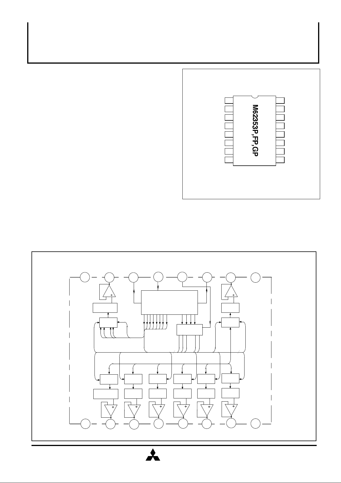
8-BIT 8CH D-A CONVERTER WITH BUFFER AMPLIFIERS
DESCRIPTION
The M62353 is an integrated circuit semiconductor of CMOS
structure with 8 channels of built-in D-A converters with output
buffer operational amplifiers.
The 3-wire serial interface method is used for the transfer
format mum wiring.
It is able to cascading serial use with Do terminal.
The output buffer operational amplifier operates in the whole
voltage range from power supply to ground for both
FEATURES
•12bit serial data input(3-wire serial data transfer method)
•Highly stable output buffer operational amplifier allow operation
in the all voltage range from power supply to ground.
APPLICATION
Adjustment/control of industrial or home-use electronic
equipment,such as VTR camera,VTR set,TV,and CRT
PIN CONFIGURATION (TOP VIEW)
Vss
Ao2
Ao3
Ao4
Ao5
Ao6
Ao7
VDD
1
2
3
4
(VrefL)
(VrefU)
Outline 16P4(P)
16P2N-A(FP)
16P2E-A(GP)
16
15
14
13
125
116
107
98
GND
Ao1
DI
CLK
LD
DO
Ao8
Vcc
BLOCK DIAGRAM
GND
16
BUFFER
OP AMP
1
Vss
(VrefL)
Ao1
15
-
8-BIT
R-2R D-A
Ch1
8-BIT
LATCH
.....
(8)
8-BIT
LATCH
Ch2
8-BIT
R-2R D-A
-
2
Ao2
DI
CLK
14 13 12
12-BIT SHIFT REGISTER
(8)
(8)
4
L
5
D-A
--
4
L
3
D-A
3
Ao3 Ao4
LD Do
D11
ADDRESS
DECODER
....
L
6
D-A
5
Ao5
11
L
D-A
--
6
Ao6
Ao8
10
-
D-A
8
L
(8)
L
7
D-A
-
7
Ao7
Vcc
9
8
VDD
(VrefU)
MITSUBISHI
ELECTRIC
( / 6 )
1
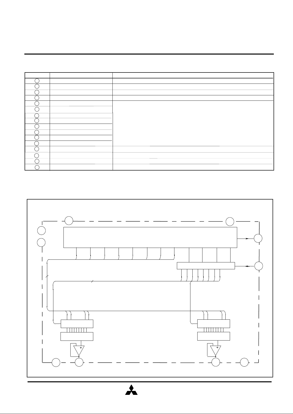
EXPLANATION OF TERMINALS
(VrefL)
Pin No. Symbol
14
11
13
12
15
2
3
4
5
6
7
10
9
16
8
1
DI
DO
CLK
LD
Ao1
Ao2
Ao3
Ao4
Ao5
Ao6
Ao7
Ao8
Vcc
GND
VDD
Vss
MITSUBISHI<Dig.Ana.INTERFACE>
M62353P,FP,GP
8-BIT 8CH D-A CONVERTER WITH BUFFER AMPLIFIERS
Function
Serial data input terminal
Serial data output terminal
Serial clock input terminal
LD terminal input high level than latch circuit data load
8-bit D-A converter output terminal
Power supply terminal
Digital and analog common GND
D-A converter upper reference voltage input terminal
D-A converter lower reference voltage input terminal
BLOCK DIAGRAM FOR EXPLANATION OF TERMINALS
Vcc
9
DI
14
CLK
13
D0
D1
8
............
D0
1
8-BIT
LATCH
8-BIT
R-2R D-A
D2
8
D7
...................................................................................................
12-BIT SHIFT REGISTER
D4
D3
.............................................8
..............................................
D5
D6 D7
D8
D9
D10 D11
ADDRESS DECODER
21
3
5 6 7
4
............
D0
8-BIT
LATCH
8-BIT
R-2R D-A
--
GND
16
D0
11
LD
12
8
D7
8
VDD
(VrefU)
15
Ao1
MITSUBISHI
ELECTRIC
10
Ao8
1
VSS
2
( / 6 )

MITSUBISHI<Dig.Ana.INTERFACE>
M62353P,FP,GP
8-BIT 8CH D-A CONVERTER WITH BUFFER AMPLIFIERS
DIGITAL DATA FORMAT
LAST
LSB
D0 D1 D2 D3 D4 D5 D6 D7 D8 D9
DAC DATA
D0 D1 D2 D3 D4 D5 D6 D7 D-A output
0
1
0
1
0
0
1
1
0
0
0
0
0
0
0
0
0
0
0
0
0
0
0
0
0
0
0
0
0
0
0
0
DAC SELECT DATA
(VrefU-VrefL)/256X1+VrefL
(VrefU-VrefL)/256X2+VrefL
(VrefU-VrefL)/256X3+VrefL
(VrefU-VrefL)/256X4+VrefL
D10
FIRST
MSB
D11
D9
1
1
0
0
0
0
1
1
1
1
0
0
0
0
1
1
1
1
1
1
D10 D11
0
0
1
1
0
0
1
1
0
0
1
1
0
0
1
1
0
1
D8
0
0
0
0
0
0
0
0
1
1
1
1
1
1
1
1
TIMING CHART (MODEL)
1
1
0
1
0
1
0
1
0
1
0
1
0
1
0
1
0
1
1
1
Don’t care
Ao1 selection
Ao2
Ao3
Ao4
Ao5
Ao6
Ao7
Ao8
Ao9
Ao10
Ao11
Ao12
Don’t care
Don’t care
Don’t care
1
1
DAC selection
1
1
(VrefU-VrefL)/256X255+VrefL
1
1
VrefU
*VrefU=VDD
VrefL=Vss
DI
CLK
LD
D-A
OUTPUT
MSB
D11 D10
D9 D8
MITSUBISHI
ELECTRIC
D2
D1
LSB
D0
( / 6 )
3

MITSUBISHI<Dig.Ana.INTERFACE>
M62353P,FP,GP
8-BIT 8CH D-A CONVERTER WITH BUFFER AMPLIFIERS
ABSOLUTE MAXIMUM RATINGS
Symbol Ratings
Vcc
VDD
VIN Input voltage
Vo
Pd
Topr
Tstg
Supply voltage
D-A converter upper reference voltage
Output voltage
Power dissipation
Operating temperature
Storage temperature
Parameter
ELECTRICAL CHARACTERISTICS
Digital part(Vcc,VrefU=+5V±10%,Vcc≥VrefU,GND,VrefL=0V,Ta=-20°C~+85°C, unless otherwise noted)
Symbol
Vcc
Icc
IILK
VIL
VIH
VOL
VOH
Supply voltage
Circuit current
Input leak current
Input low voltage
Input high voltage
Output low voltage
Output high voltage
Parameter
CLK=1MHz operation
IOA=0µA
VIN=0~Vcc
IOL=2.5mA
IOH=-400µA
Conditions
Test conditions
-0.3~7.0
-0.3~7.0
-0.3~Vcc+0.3
-0.3~Vcc+0.3
450(P)/300(FP)/150(GP)
-20~+85
-55~+125
Limits
Min.
4.5
-10
0.8Vcc
Typ.
5.0
1.6
Vcc-0.4
Max.
5.5
3.2
10
0.2Vcc
0.4
Unit
V
V
V
V
mV
°C
°C
Unit
V
mA
µA
V
V
V
V
Analog part(Vcc,VrefU=+5V±10%,Vcc≥VrefU,Ta=-20°C~+85°C, unless otherwise noted)
Symbol
IDD
VDD
Vss
VAO
IAO
SDL
SL
SZERO
SFULL
CO
RO
Parameter
Current dissipation
D-A converter upper reference
voltage range
D-A converter lower reference
voltage range
Buffer amplifier
output voltage range
Buffer amplifier
output drive range
Differential nonlinearity error
Nonlinearity error
Zero code error
Full scale error
Output capacitive load
Buffer amplifier output impedance
VrefU=5V,VrefL=0V
Data condition;at maximum current
The output dose not necessarily be the value
within the reference voltage setting range.
The output value is determined by the buffer
amplifier output voltage range(VAO)
IOA=±100µA
IOA=±500µA
Upper side saturation voltage=0.3V
Lower side saturation voltage=0.2V
VrefU=4.79V
VrefL=0.95V
Vcc=5.5V(15mV/LSB)
Without load(IOA=±0)
Test conditions
Min.
3.5
GND
0.1
0.2
-1
-1.0
-1.5
-2
-2
Limits
Typ.
0.9
5
Max.
1.7
Vcc
Vcc-3.5
Vcc-0.1
Vcc-0.2
1
1.0
1.5
2
2
0.1
Unit
mA
V
V
V
mA
LSB
LSB
LSB
LSB
µF
Ω
MITSUBISHI
ELECTRIC
( / 6 )
4
MITSUBISHI<Dig.Ana.INTERFACE>
M62353P,FP,GP
8-BIT 8CH D-A CONVERTER WITH BUFFER AMPLIFIERS
AC CHARACTERISTICS(Vcc,VrefU=+5V±10%,Vcc≥VrefU,GND,VrefL=0V,Ta=-20~+85°C, unless otherwise noted)
Symbol
tCLK
tCKH
tCR Clock rise time
tCF
tDCH
tCHD
tCHL
tLDC
tLDH
tDO
tLDD
Clock "L"pulse width
Clock "H"pulse width
Clock fall time
Data setup time
Data hold time
LD setup time
LD hold time
LD "H" pulse width
Data output delay time
D-A output setting time
Parameter
Test conditions
CL≤100pF
CL≤100pF VAQ:0.5 4.5V
The time until the output becomes the
final value of 1/2 LSB
Min Typ
200
200
30
60
200
100
100
70 350
Limits
Max
200
200
300
Unit
ns
ns
ns
ns
ns
ns
ns
ns
ns
ns
µs
TIMING CHART
CLK
DI
LD
D-A
OUTPUT
DO
OUTPUT
tCR tCF
tCKL
tDCH
tCKH
tCHD
tDO
tLDC
tLDH
tCHL
tLDD
MITSUBISHI
ELECTRIC
( / 6 )
5

TYPICAL CHARACTERISTICS
MITSUBISHI<Dig.Ana.INTERFACE>
M62353P,FP,GP
8-BIT 8CH D-A CONVERTER WITH BUFFER AMPLIFIERS
UPPER SIDE SATURATION VOLTAGE VS.
OUTPUT SOURCE CURRENT
150
100
50
0
200
0
OUTPUT SOURCE CURRENT
400 600 800 1000
IAOD(µA)
SATURATION VOLTAGE VS.OUTPUT CURRENT
LOWER SIDE SATURATION VOLTAGE VS.
150
100
50
0
OUTPUT SINK CURRENT
200 400 600 800
0
OUTPUT SINK CURRENT
IAOD(µA)
1000
MITSUBISHI
ELECTRIC
( / 6 )
6
 Loading...