8-BIT 2CH D-A CONVERTER WITH BUFFER AMPLIFIERS
GENERAL DESCRIPTION
The M62342P,FP is a CMOS 2 channel D-A converter
with output buffer amplifiers.
It can communicate with a microcontroller via few wiring
thanks to the adoption of the three-line DI,CLK,LD.
The output buffer amplifier employs AB class output with
sinking and sourcing capability of more than 1.0mA , and
an output voltage range is nearly between ground and
Vcc.
FEATURES
• 10bit serial data input (3-wire serial transfer method)
• Wide output voltage range
Nearly between ground and Vcc(0 to 5V)
• High output current drive capability
over ±1.0mA
MITSUBISHI <STD. LINEAR ICs>
M62342P,FP
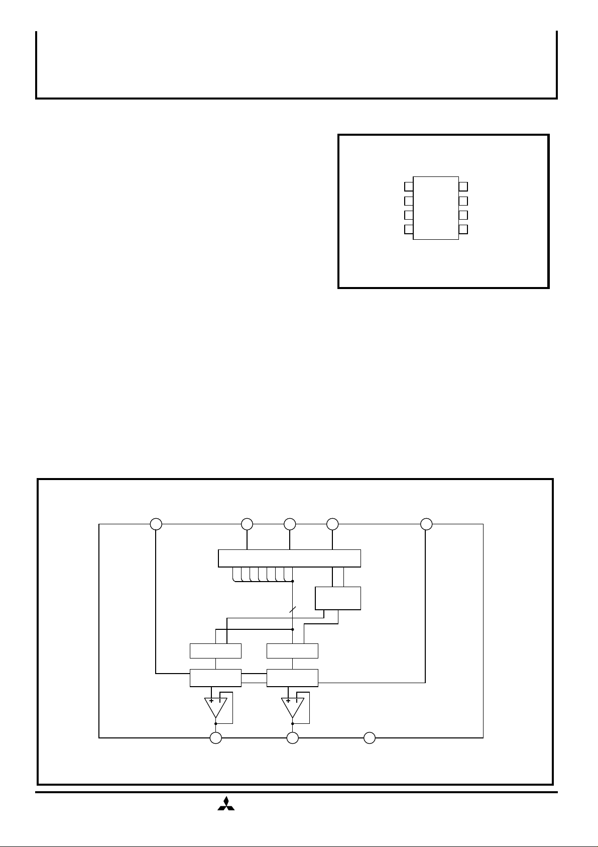
PIN CONFIGURATION (TOP VIEW)
Ao1
Ao2
N.C.
VCC
Outline
1
2
3
4
8
M62342
L D
7
CLK
6
D I
5
GND
8P4 (P)
8P2S-A (FP)
APPLICATION
Conversion from digital data to analog control data for both consumer and industrial equipment.
Gain control and automatic adjustment of DISPLAY-MONITOR or CTV.
BLOCK DIAGRAM
VCC
L D CLK
4 8 7
10-BIT SHIFT REGISTER
8bit Latch
8bit upper
segment R-2R
8bit Latch
8bit upper
segment R-2R
8
D I
6
ADDRESS
DECODER
GND
5
1
Ao1
2
Ao2
N.C.
MITSUBISHI ELECTRIC
3
2000-8-31.revB
( / 5 )
1

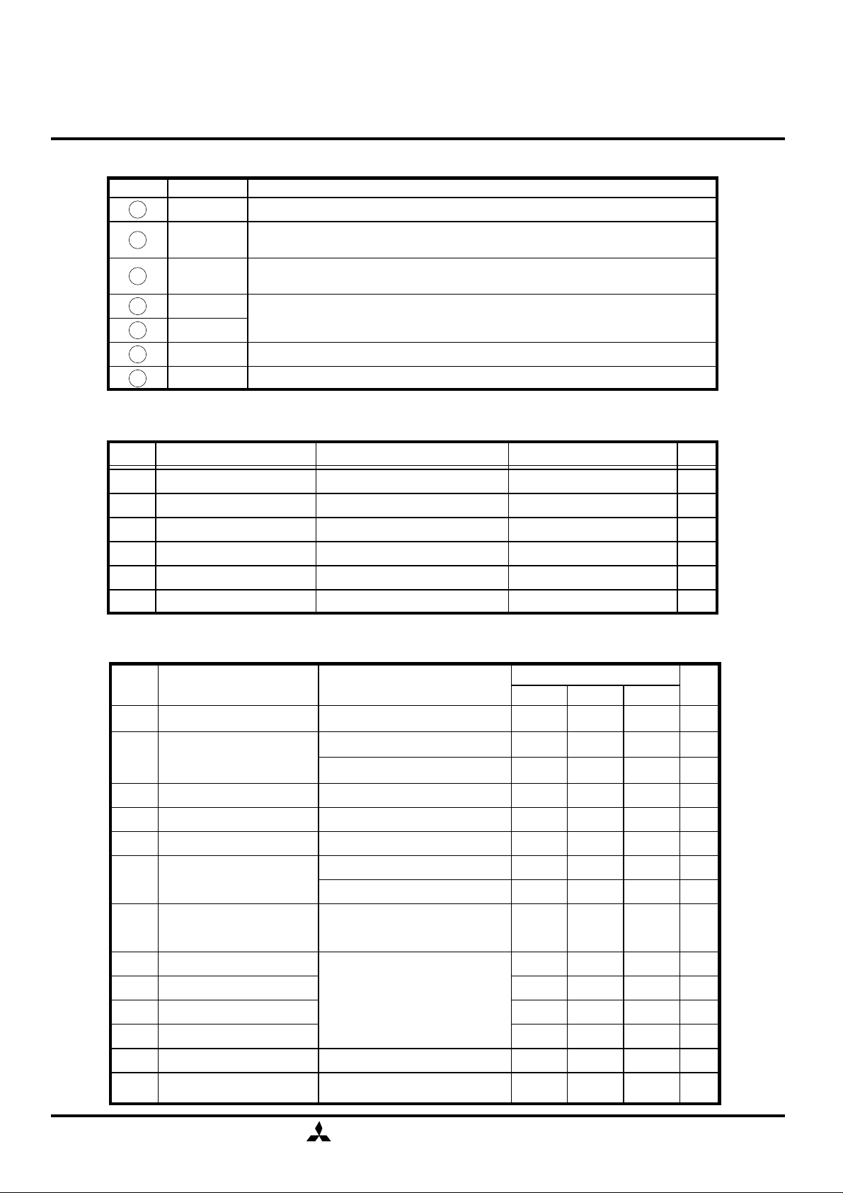
EXPLANATION OF TERMINALS
PIN No.
6
Symbol
D I
Serial data input terminal
MITSUBISHI <STD. LINEAR ICs>
M62342P,FP
8-BIT 2CH D-A CONVERTER WITH BUFFER AMPLIFIERS
F u n c t i o n
7
8
1
2
4
5
CLK
L D
Ao1
Ao2
Vcc
GND
Shift clock input terminal. Input signal at DI pin is input to 10-bit shift register at
rise of shift clock pulse.
When H-level signal is input to this terminal,the value stored in 10-bit shift
register is loaded in decoder and D-A converter output register.
8bit D–A converter output terminal
Power supply terminal
GND
ABSOLUTE MAXIMUM RATING
Symbol
Vcc
Vin
Vo
Pd
Topr
Tstg
Parameter Conditions UnitRatings
Supply voltage
Input voltage
Output voltage
Power dissipation
Operating temperature
Storage temperature
-0.3 to 7.0
-0.3 to VCC+0.3
-0.3 to VCC+0.3
417 (DIP) / 272 (FP)
-20 to +85
-55 to +125
V
V
V
mW
°C
°C
ELECTRICAL CHARACTERISTICS (VCC=+5V±10%,GND=0V,Ta=–20 to 85°C unless otherwise noted)
Symbol
V
CC
ICC
IILK
VIL
VIH
V
AO
IAO
SDL
SL
SZERO
SFULL
Co
Ro
Parameter
Supply voltage
Supply current
Input leak current
Input low voltage
Input high voltage
Buffer amplifier output
voltage range
Buffer amplifier output
drive range
Differential nonlinearity
Nonlinearity
Zero code error
Full scale error
Output capacitive load
Buffer amplifier
output impedance
Test conditions
CLK=1MHz, IAO=0µA
DACdata:6Ah(at maximum current)
DI=CLK=LD=GND,IAO=0µA
IN=0 to VCC
V
I
AO=±100µA
I
AO=±500µA
Upper side saturation voltage=0.3V
Lower side saturation voltage=0.2V
VCC=5.12V (20mV/LSB)
without load
(IAO=0)
Min Typ Max
-10 10
0.5VCC
-1.0 1.0 mA
-1.0 1.0
-1.5 1.5
-2.0 2.0
-2.0 2.0
Ratings
2.7 5.0 5.5
0 0.7 2.5
0
0.1
0.2
0.5 1.6
0.2V
V
CC-0.1
CC-0.2
V
0.1
5.0
CC
Unit
V
mA
mA
µA
V
V
V
V
LSB
LSB
LSB
LSB
µF
Ω
MITSUBISHI ELECTRIC
2000-8-31.revB
( / 5 )
2
 Loading...