Mitsubishi M62339FP, M62334P, M62334FP Datasheet

MITSUBISHI <STD. LINEAR ICs>
S
t
r
segme
2
3Ao4
M62334P/FP
M62339P/FP
8-BIT 4CH I2C BU S D -A CONVERTER WITH BUFFER A MPLIFIER
DESCRIPTION
The M62334/M62339 is an integrated circui
semiconductor of CMOS structure with 4 channels of built
in D-A converters with output buffer operational amplifiers.
The input is 2-wires serial method is used for the transfer
format of digital data to allow connection with a
microcomputer with minimum wiring.
The output buffer operational amplifier employs AB class
output circuit with sync and source drive capacity of 1.0mA
or more,and it operates in the whole voltage range from
Vcc to ground.
The M62333 and the M62338 differ only in their slave
address.
FEATURES
• Digital data transfer format
2
I
C BUS serial data method
• Output buffer operational amplifier
it operates in the whole voltage range from Vcc to
ground.
• High output current drive capacity
±1.0mA over
APPLICATION
Conversion from digital data to analog control data fo
home-use and industrial equipment.
Signal gain control or automatic adjustment of DISPLAY-
MONITOR or CTV.
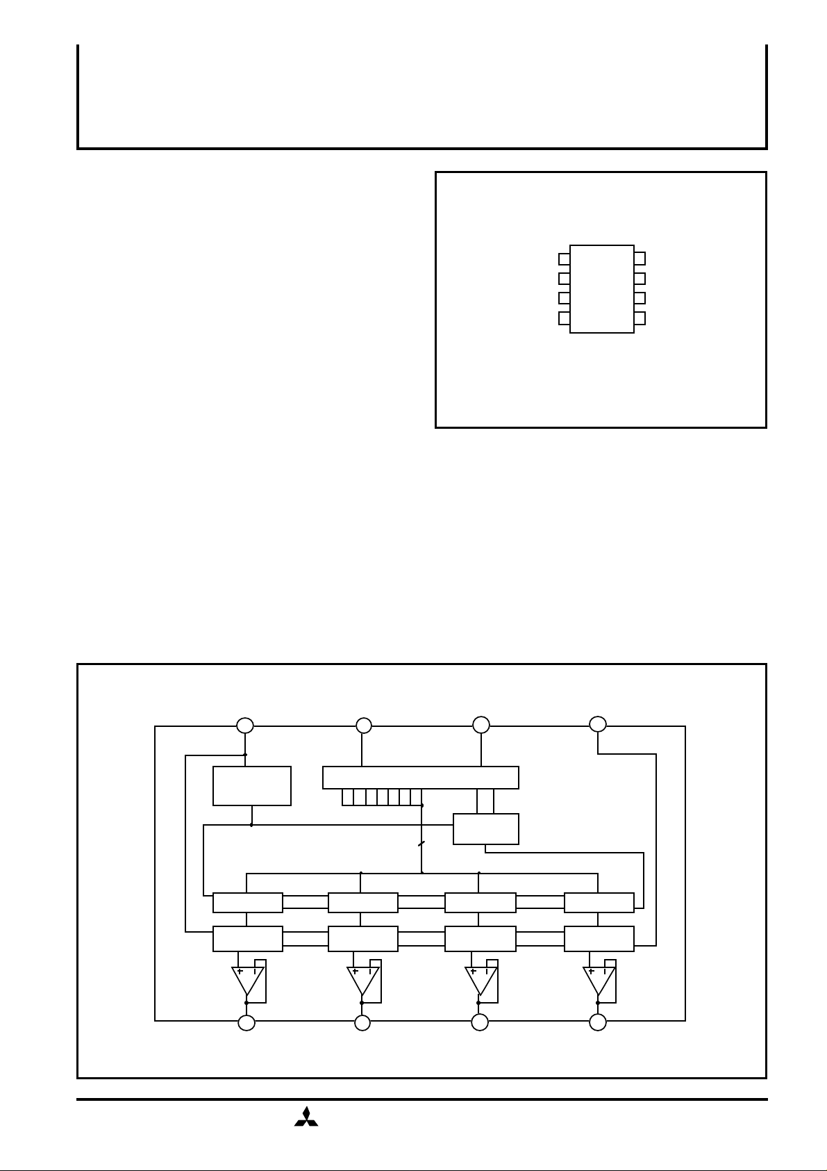
PIN CON FIGU RATION(TOP VIEW)
1
Ao1
2
Ao
3
Ao
4
Outline 8P4 (P)
M62339
8
M62334
8P2S-A (FP)
Vcc
7
SCL
6
SDA
5
GND
BLOCK DIA GRAM
Vcc
8
POWER ON
RESET
8bit Latch
8bit upper
segment R-2R
1
Ao1
SCL SDA GND
7 6 5
I2C BUS TRANSCEIVER
CHANNEL
DECODER
8
8bit Latch
8bit upper
nt R-2R
8bit Latch
8bit upper
segment R-2R
2
Ao2
3
Ao3
8bit Latch
8bit upper
segment R-2R
4
Ao4
MITSUBISHI ELECTRIC
980714 rev.E ( / 6 )
1

P
8-BIT 4CH I2C BUS D-A CONVERTER WITH BUFFER AMPLIFIER
S
P
voltage
Parameter
Conditions
–0.3 to 7.0
–0.3 to Vcc+0.3
–20 to 85
–55 to 125
UnitVVVmW
°C
417 (DIP) / 272 (FP)
–0.3 to Vcc+0.3
°C
Buffer amplifier
output inpedance
867
512
SDA
SCL
Ao1
Vcc
GND
Ao2
Ao3
4
Ao4
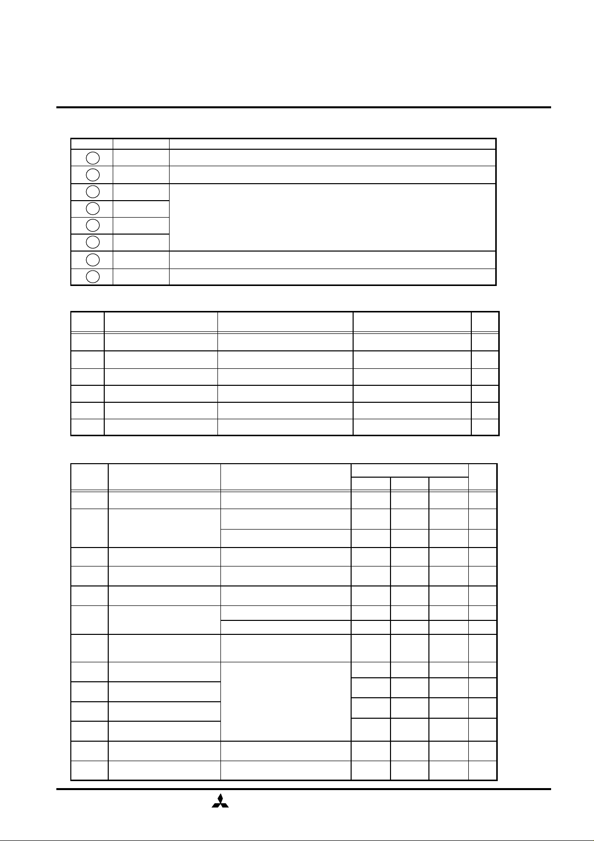
EXPLANATION OF TERMINALS
Pin No. Symbol Function
Serial data input terminal
Serial clock input terminal
MITSUBISHI <STD. LINEAR ICs>
M62334P/F
M62339P/F
3
8-bit resolution D-A converter output terminal
Power supply terminal
GND terminal
ABSOLUTE MAXIMUM RATING
Symbol
Vcc
Vin
Vo
Pd
Topr
Tstg
Supply
Input voltage
Output voltage
Power dissipation
Operating temperature
Storage temperature
Ratings
ELECTRICAL CHARACTERISTICS (Vcc=+5V±10%,GND=0V,Ta=–20 to 85°C unless otherwise noted)
Symbol
Vcc
Icc Supply current
IILK
Parameter Test conditions
Suplly voltage
Input leak current
CLK=500kHz Operation, IAO=0µA
Data : 6Ah (at maximum current )
SDA=SCL=GND,IAO=0µA
VIN=0 to Vcc
Ratings
MIN TYP MAX
2.7 5.0 5.5
0 1.4 3.0
0 0.9 2.0
–10 10
Unit
V
mA
mA
µA
VIL
VIH
VAO
IAO
SDL
SL
SZERO
SFULL
Co
Ro
Input low voltage
Input high voltage
Buffer amplifier output
voltage range
Buffer amplifier output
drive range
Differential nonlinearity
Nonlinearity
Zero code error
Full scale error
Output capacitative load
IAO=±100µA
IAO=±500µA
Upper side saturation voltage=0.3V
Lower side saturation voltage=0.2V
VCC=5.12V(20mV/LSB)
without load (IAO=0)
MITSUBISHI ELECTRIC
0
0.8VCC
0.1
0.2 V
–1.0 1.0 mA
–1.0 1.0
–1.5 1.5
–2.0 2.0
–2.0 2.0
5.0
0.2VCC V
VCC
VCC-0.1
VCC-0.2
0.1
V
V
LSB
LSB
LSB
LSB
µF
Ω
980714 rev.E ( / 6 )
2
 Loading...