Mitsubishi M62320P, M62320FP Datasheet

GENERAL DESCRIPTION
The M62320P/FP is a CMOS 8-bit I/O expander which has
serial to parallel and parallel to serial data converting
functions.
It can communicate with a microcontroller via few wiring
2
thanks to the adoption of the two-line I
C BUS.
Parallel data I/O terminal can be set to input or output
mode alternatively in individual bits.
Maximum 8 ICs can be connected to a bus by using three
chip-select pins, so that it is possible to handle up to 64 bits
data.
FEATURES
• Simple two-line (SCL and SDA) communication with a
microcontroller.
• 8-bit data conversion between serial and parallel by
2
C BUS.
I
• Built-in power-on reset.
APPLICATION
I/O port expansion for a microcontroller.
Data conversion between serial and parallel in
microcontroller peripherals.
MITSUBISHI < STD. LINEAR ICs >
M62320P,FP
16
15
14
13
12
11
10
2
CS0
CS1
CS2
V
DD
D7
D6
D5
D4
9
8-BIT I/O EXPANDER for I C BUS
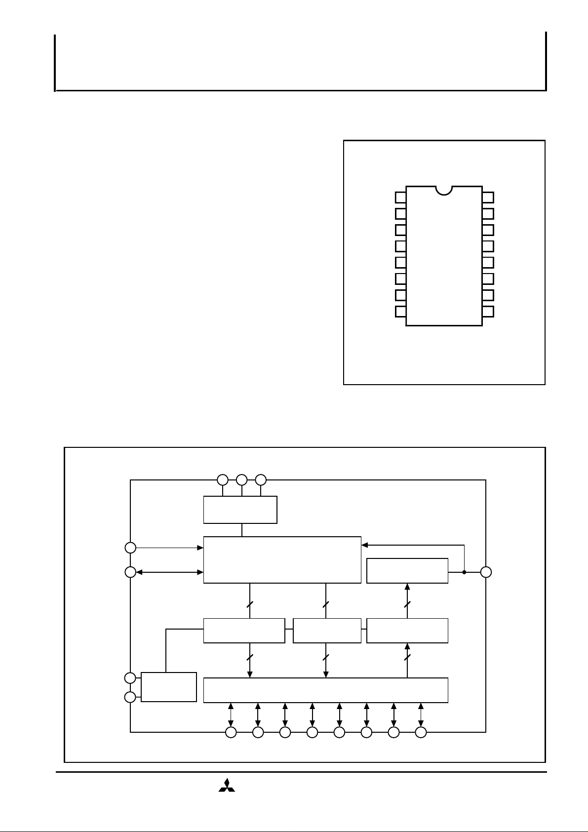
PIN CONFIGURATION(TOP VIEW)
SO
1
SCL
2
SDA
3
D0
4
D1
5
D2
6
D3
7
GND
8
Outline 16P4(P)
M62320P,FP
16P2N(FP)
BLOCK DIAGRAM
SCL
SDA
VDD
GND
2
3
13
POWER-ON
RESET
8
CS0 CS1 CS2
16
1415
CHIP-SELECT
2
I C BUS
TRANSCEIVER
Output Data
8
OUTPUT DATA
LATCH
8 8
1112
D7
I/O SETTING
DATA LATCH
Å@
I/O PORT
10
Input/Output
8
8
SHIFT
REGISTER
8
INPUT DATA
LATCH
Input Data
45679
D0D1D2D3D4D5D6
1
SO
MITSUBISHI ELECTRIC
2/20,1998(rev) ( / 9 )
1

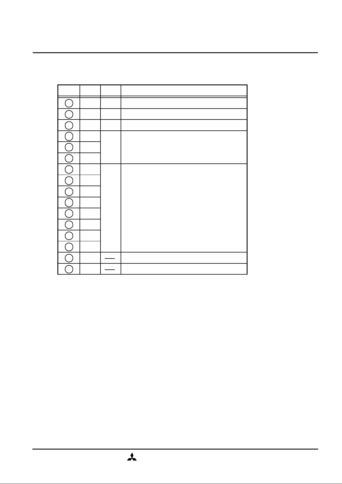
PIN DESCRIPTION
MITSUBISHI < STD. LINEAR ICs >
M62320P,FP
8-BIT I/O EXPANDER for I C BUS
2
16
15
14
10
11
12
13
Symbol
2
SCL Serial clock input
3
SDA
1
4
5
6
7
9
SO
CS0
CS1
CS2
D0
D1
D2
D3
D4
D5
D6
D7
V
DD
I/O
Input
Input/
Output
Output
Input
Input/
Output
Serial data input/output
Serial data output
Chip select data input
Parallel data input/output
Power supply
FunctionPin No.
GND
8
GND
MITSUBISHI ELECTRIC
2/20,1998(rev) ( / 9 )
2

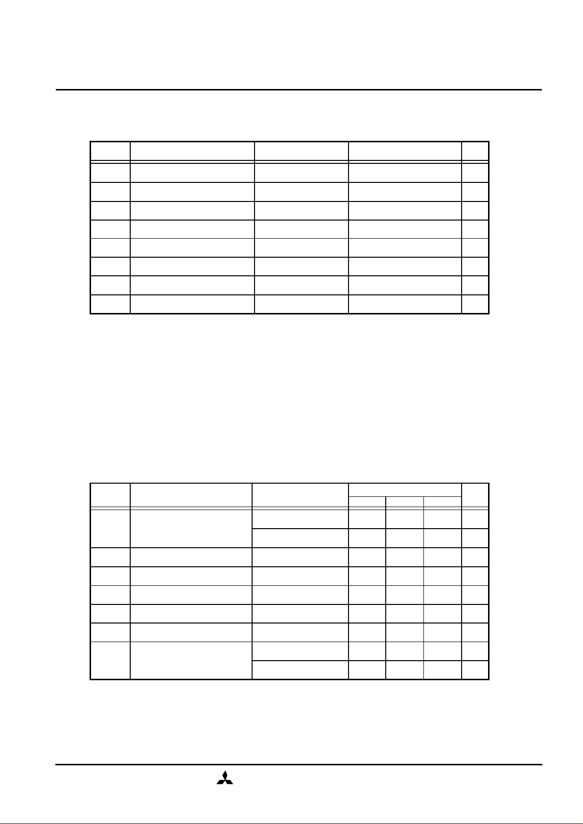
ABSOLUTE MAXIMUM RATINGS
MITSUBISHI < STD. LINEAR ICs >
M62320P,FP
8-BIT I/O EXPANDER for I C BUS
2
Symbol
VDD
VI
VO
OH
I
IOL
Pd
Supply voltage
Input voltage
Output voltage
Output current "Low"
Output current "High"
Power dissipation
Parameter
Topr Operating temperature
Tstg Storage temperature
RECOMMENDED OPERATING CONDITIONS
• Supply voltage………VDD=5V±10%
• Input high voltage……VIH=0.8VDD to VDD
• Input low voltage………VIL=0 to 0.2VDD
Conditions
D
0 to D7
D0 to D7
Ta = 25°C
Ratings
–0.3 to 7.0
–0.3 to V
–0.3 to V
DD+0.3
DD+0.3
- 5 to 0
0 to 30
1220(P) / 980(FP)
-20 to 85
-40 to 125
Unit
V
V
V
mA
mA
mW
°C
°C
ELECTRICAL CHARACTERISTICS
(VDD=5V ±10%, GND=0V,Ta=20 to 85°C, unless otherwise noted)
Symbol Parameter Conditions
VIH = VDD,VIL = GND,
f
DD
ILK Input leak current
I
VIH
V
IL
VOH
V
OL
IOL
Circuit currentI
Input high voltage
Input low voltage
Output high voltage
Output low voltage
Output current "Low"
SCL = 400kHZ
IH = VDD,VIL = GND,
V
f
SCL = stop
IOH = -1mA
I
V
V
OL = 5mA
OL = 0.4V
OL = 1.0V
Limits
Min Typ Max
0.05
0.1
-10
0.8V
DD
0.2VDD
V
DD-0.4
5
15
10
25
0.5
1.0
10
0.4
Unit
mA
µA
µA
V
V
V
V
mA
mA
MITSUBISHI ELECTRIC
2/20,1998(rev) ( / 9 )
3
 Loading...