

MITSUBISHI(Standard Linear ICs)
M62292FP
3.3V, 1.8V FIXED 2-OUTPUT VOLTAGE DC-DC CONVERTER
DESCRIPTION
M62293FP is 3.3V and 1.8V fixed stable 2-output step-down DC-DC
cost
sets because this device includes peripheral devices in small size 8pin
package.
The IC also has Reset circuit with time delay that monitors power
supply(Vcc=5V) and one regulator output(Vout1=3.3V;IN1 terminal),
therefore an application system is protected system errors.
Especially this is most suitable for application sysytem with microprocessor
and ASIC.
FEATURES
APPLICATION
( 1 / )
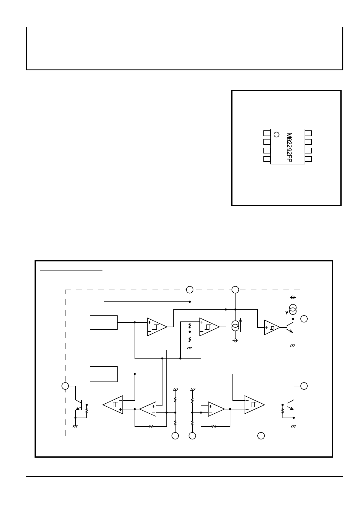
BLOCK DIAGRAM
Cout1
IN1(3.3V)
IN2(1.8V)
Cout2
VccCdGND
RESET
oscillator
(110kHz)
Vref
1.25V
IN1;3.3V
25µA
Vcc
0.6µA
PIN CONFIGURATION(TOP VIEW)
Outline 8P2S-A
converter.
It is possible to simplify peripheral circuit and to design compact and low
● 3.3V and 1.8V step-down converter
● 4 to 15V wide input supply voltage (Vcc=5V typ.)
● Reset circuit with time delay monitors
supply voltage(Vcc=5V)and regulator output (3.3V)
● 110kHz fixed frequency oscillator without peripheral devices
● 8pin SOP package
application system with microprocessor and ASIC
Cout1
GND
Cout2
Vcc
1
2
3
4
8
7
6
5
IN1
RESET
Cd
IN2
comparator
(3.3V detect) (Vcc detect)
op amp op amp
4
comparator
PWM comp.PWM comp.
000131
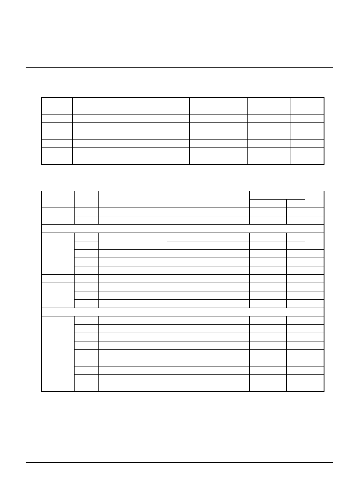
ABSOLUTE MAXIMUM RATINGS(Ta=25C,unless otherwise noted)
Supply voltage
Output current(DC-DC converter block)
Symbol
Parameter
Conditions
Ratings
Unit
VccIo16VmAPdPower dissipation
440
mWKθThermal derating
Topr
Tstg
Operating temperature
Storage temperature
-20 ~+85
-40 ~+125
˚C˚CTa=25˚C
Ta >25˚C
4.4
mW/˚C
ch1,ch2
ELECTRICAL CHARACTERISTICS(Ta=25C,Vcc=5V,unless otherwise noted)
Supply voltage
Supply current
Block
Parameter
Test condition
Limits
Unit
Vcc
Icc
4.0
V-mA
Output voltage
V
mV-Error Amp.
Input current 1
µA65KHz
Oscillator
Maximum ON duty
%
Symbol
Line regulation
Oscillator frequency
Detecting voltage 1
Detecting voltage 2
Without load
Vcc=4~12V
Vreg-L
Iin
fosc
TDUTY
Vs1
Vs2
All
Blocks
15515
150
450
110
160903.8
2.58VmV
Min.
Typ.
Max.
3.15
3.30
3.45
1.71
1.80
1.89
ch1 output
ch2 output
hysterisys voltage 1
Hysterisys voltage 2
∆Vs1
∆Vs2
Output
V
Cd output current
IPD
-0.3µADelay time
Cd=4700pF
tpd
msec
Output leakage current
Vcc=12V, Vc=12V
ICL-11VOutput saturation voltage
Io=10mA,Darlington connection
Vsat-1.2
2.0
V
Circuit
mV
RESET LOW voltage
VOL-0.2Vo1
V
5.0
2.8
1.5
Vcc=5V detection
ch1output(3.3V)detection
RESET High voltage
VOH
0.8Vo1
10
3.6
4.0
2.46
2.70503080503080520
IOCµA-25
-40
-17
Vo1
Vo2
Output current(Reset block)
IoRESET
mA6Reset circuit Block
DC-DC Converter Block
IoRESET=4mA
-1.1
-0.6
Input current 2
µA
Iin
100
300
ch1
ch2
MITSUBISHI(Standard Linear ICs)
M62292FP
3.3V, 1.8V FIXED 2-OUTPUT VOLTAGE DC-DC CONVERTER
RESET output current
( 2 / )
30
-
-
- -
Reset
Vcc=5V, Vo=1/2 X Vcc
4
-
-
V
000131

RESET BLOCK timing chart
5V
3.85V
3.80V
3.3V
2.63V
2.58VtdVo1tdtd0V0V
0V
t
t
MITSUBISHI(Standard Linear ICs)
M62292FP
3.3V, 1.8V FIXED 2-OUTPUT VOLTAGE DC-DC CONVERTER
( 3 / )
-3
td : RESET Delay Time •••
td(msec) = 2.13 ×10 × Cd(pF)
t
4
000131

APPLICATION CIRCUIT (3.3V and 1.8V 2-output voltage DC-DC converter
Vcc
Cout1
GND
+
M62292FP
Co1R1L1D1Q1
R3L2D2
Cd
R4
approximately greater than "Ipk".
TON
Expressions
Ipk
MITSUBISHI(Standard Linear ICs)
M62292FP
3.3V, 1.8V FIXED 2-OUTPUT VOLTAGE DC-DC CONVERTER
( 4 / )
VIN(5V)
Cin
VOUT1(3.3V)
VOUT2(1.8V)
Co2
THE EXPRESSION OF CIRCUIT CONSTANTS
+
+
Constants
TOFF
(TON+TOFF)MAX
TOFF(MIN)
TON(MAX)
IN1
IN2
RESET
MCU etc.
1.8V LINE
VO+VF
VIN - VCE(sat) - VO
1
fosc
( TON + TOFF ) /
fosc:110KHz(Vcc=5V)
1
fosc
Cout2
1 +
(
- TOFF
3.3V LINE
TON
TOFF
R2
Q2
)
L(MIN)
note:
• VF : Forward voltage drop of an external diode
• Vsat : Output saturation voltage of an external switching transistor.
• ∆IO : Set to 1/3 to 1/5 of maximum output current.
• Choose an external transistor, diode and inductor with peak current rating
( VIN - VCE(sat) - VO ) × TON(MAX)
Io +
∆Io
1
2
4
∆Io
000131
 Loading...