MITSUBISHI SEMICONDUCTOR < STANDERD LINEAR IC >
note: GND terminal is connected to emitter terminal
as M62281FP in IC inside.
And Vcc terminal is connected to collector
terminal as M62281FP in IC inside.
GENERAL PURPOSE CURRENT MODE PWM CONTROL ICGENERAL PURPOSE CURRENT MODE PWM CONTROL IC
DESCRIPTION
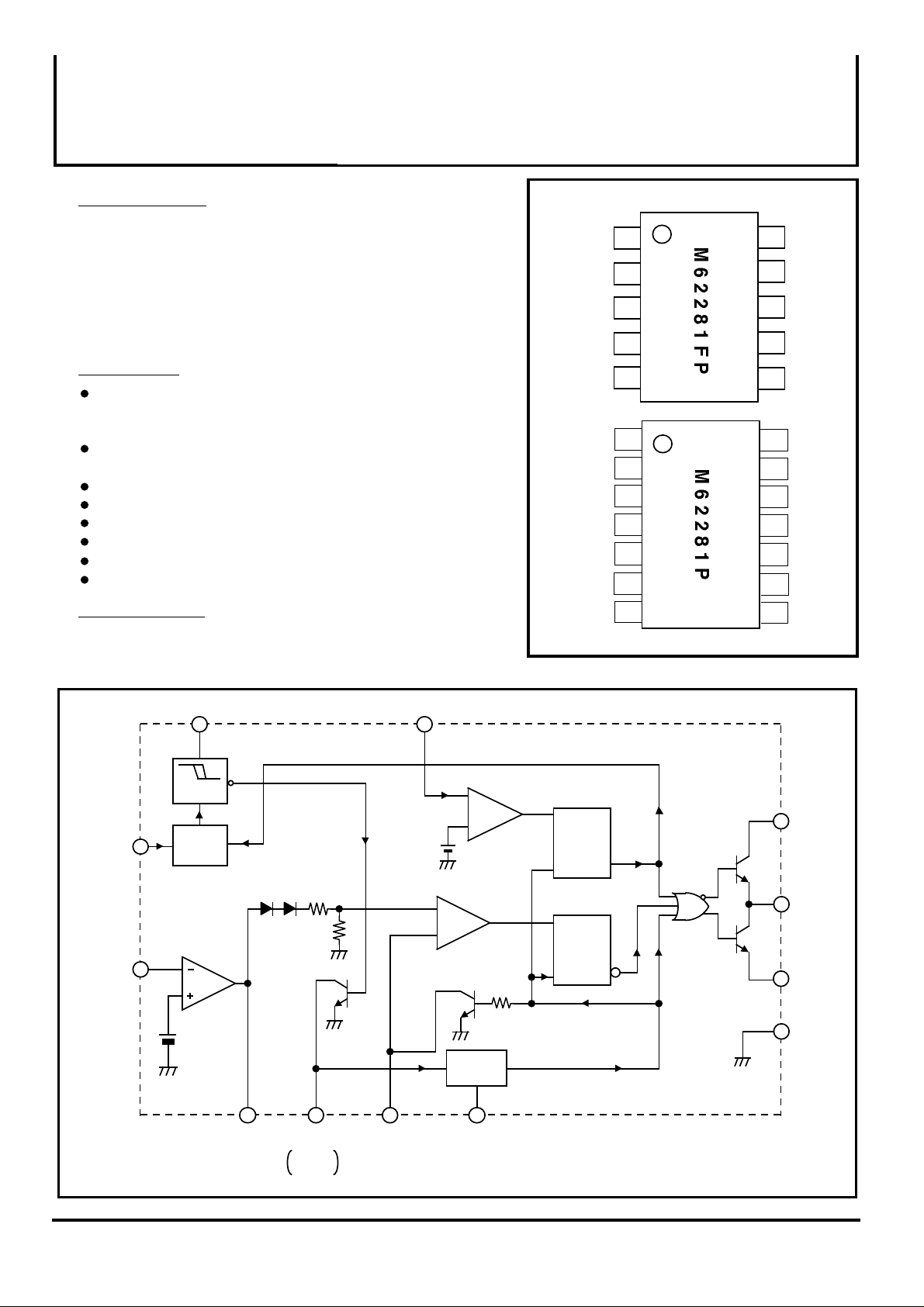
M62281P/FP is designed as a high speed current mode
PWM control IC.
This small10 pin package contains many functions and
protection circuits allowing simpler peripheral circuit and
compact set design.
This IC can operate high speed switching (700kHz max.)
with high speed current sense comparator and current
limiting circuit.
FEATURES
700kHz applicable to MOS-FET
• Output current Io(peak) = ±1A
• Totem pole output
CURRENT SENSE terminal separate form CLM terminal makes
SMPS strong in noise.
High speed pulse-by-pulse current limiting
Timer type latch protection circuit with OVP(external reset is possible)
Soft start operation is possible (with dead time control)
Built-in OPAmp for feedback control (photo coupler can be driven)
Small start-up current 180µA
Start-up voltage 12.5V, Stop voltage 8.3V
APPLICATION
• Switching Regulator
• DC-DC converter
M62281P/FP
PIN CONFIGURATION (TOP VIEW)
VOUT
GND
CLM
CURRENT
SENSE
VOUT
EMIT
GND
CLM
CURRENT
SENSE
1
2
3
4
5
CF
1
2
3
4
5
6
CF
7
N.C 8
M62281P/FP
OUTLINE 10P2N-A
OUTLINE 14P4
10
9
8
7
6
14
13
12
11
10
9
Vcc
EA IN
EA OUT
CT
SOFT
COLLECT
Vcc
EA IN
EA OUT
CT
SOFT
N.C
CT
(OVP)
EA IN
Vcc CLM
UVLO
TIMER
LATCH
2.5V
EA
OUT
SOFT
DUTY
SET-UP
SENSE
CS
COMP
CLM
COMP
0.2V
OSC.
CFCURRENT
S
CLM
LATCH
R
R
PWM
LATCH
S
:note
COLLECT
VOUT
:note
EMIT
GND
( / 9 )
1

MITSUBISHI SEMICONDUCTOR < STANDERD LINEAR IC >
M62281P/FP
GENERAL PURPOSE CURRENT MODE PWM CONTROL IC
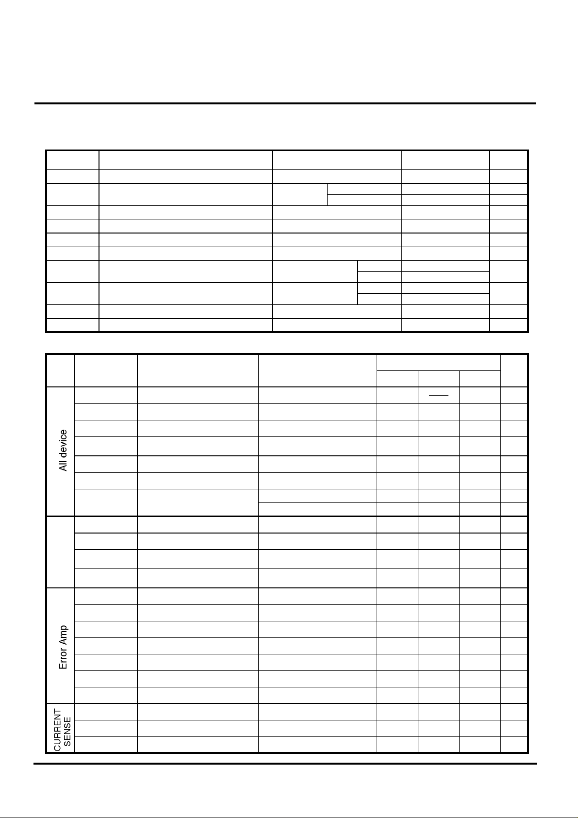
ABSOLUTE MAXIMUM RATINGS (Ta=25˚C, unless otherwise noted)
Symbol Parameter Condition Rating Unit
Vcc Supply voltage 36 V
IOUT Output current
VCT
Pd Power dissipation
Ktheta Thermal derating
CT terminal Supply voltage
EA IN terminal Supply voltageVEA IN
CLM terminal Supply voltageVCLM
CURENT SENSE terminal Supply voltageVCS
Operating temperatureTopr
Storage temperatureTstg
Ta≥25˚C
Continuous
P
FP
P
FP
36 V
10
- 0.3 ~ + 4.0
- 0.3 ~ + 5.8
1500
440
12
3.52
- 20 ~ + 85
- 40 ~ + 150
mA150
mW
mW/˚C
A1.0Peak
V
V
V
˚C
˚C
ELECTRICAL CHARACTERISTICS (Ta=25˚C, Vcc=14V, unless otherwise noted)
Limits
Block
CT
Symbol
Vcc Supply voltage range 35 V
∆Vcc
IccL
IccO Operating current
IccOFF Timer latch circuit current
VTHCTH
VTHCTL
ITIMEOFFIN
ITIMEOFFOUT
VB Reference voltage
IB Input bias current
AVO Open loop gain
fT Unity gain bandwidth
IOS Output source current
VOm + Output voltage (High)
VOm - Output voltage (Low)
AVCS CS term. input voltage gain
IB Input bias burrent
TPDCS CS term. delay time Delay time to output
Parameter Test condition
Operation stop voltage
Start-up and stop
voltage difference
Stand-by current Vcc=Vcc(START) - 0.5V
Vcc=14V
Vcc=Vcc(STOP) + 0.2V
CT term."H" threshold voltage
CT term."L" threshold voltage
CT term. input current
(timer off mode)
CT term. output current
(timer on mode)
Min
Vcc
(STOP)
11.5 12.5 13.5Vcc(START) Operation start-up voltage
7.6 8.3 9.0
3.5 4.2 5.1 V
90 180 270
7.5 13 19 mA
0.9 2.0 3.00.9
3.5 4.0 4.5
Typ Max
Unit
V
VVcc(STOP)
µA
mA
mA1.8 2.70.8
V
V0.4 0.7 1.0
µA70 115 165
µA-33 -14 -5
V2.4 2.5 2.6
nA-300 -100 0
dB70
MHz1
µA-460 -370 -240
V5.3 5.8 6.25
V0 0.2 0.35
V/V3.0
µA-5 -1
nS150
( / 9 )
2

MITSUBISHI SEMICONDUCTOR < STANDERD LINEAR IC >
M62281P/FP
GENERAL PURPOSE CURRENT MODE PWM CONTROL IC
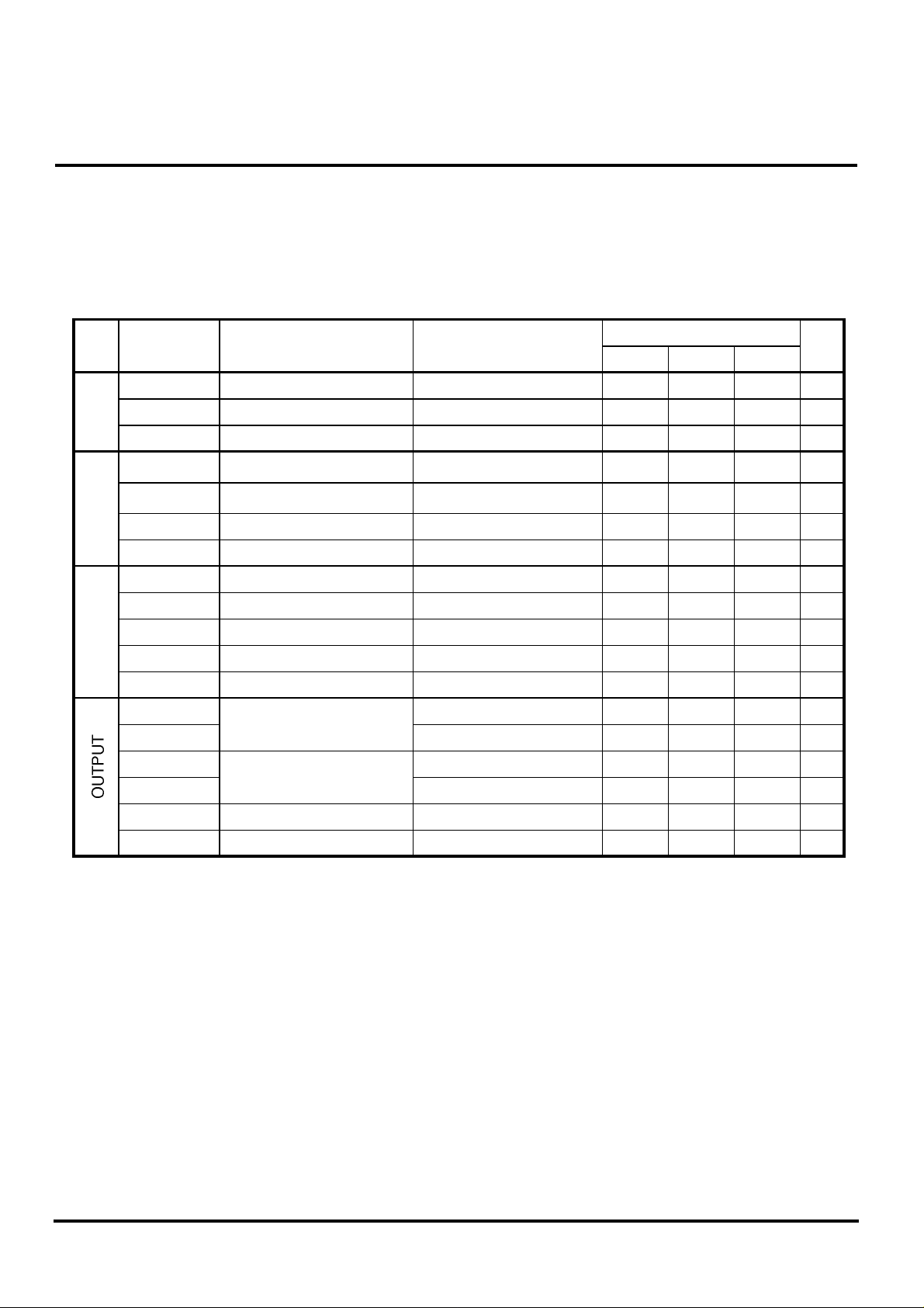
ELECTRICAL CHARACTERISTICS (Ta=25˚C, Vcc=14V, unless otherwise noted)
Block
C
L
M
S
O
F
T
OSC.
Symbol
VTHCLM
Parameter Test condition
CLM term. threshold voltage
IOUTCLM CLM term. output current
TPDCLM
VSOFT(0%)
VSOFT(50%)
Duty Max
ISOFT
foscmax
fosc
VOSCH
VOSCL
∆VOSC
CLM term. delay time
Soft term. input voltage range
to set 0% duty
Soft term. voltage
when 50% duty
Maximum duty
Soft term. input current
Maximum oscillation frequency
Oscillation frequency
Oscillation upper limit voltage
Oscillation lower limit voltage
Oscillation voltage
VOL1
Output low voltage
VOL2
VOH1
Output high voltage
VOH2
TRISE
Output voltage rise time
Output voltage fall timeTFALL
VCLM=0V
Delay time to output
Soft term. input voltage range
to set 0% duty
CF= 270pF
CF= 270pF
CF= 270pF
CF= 270pF
Vcc=14V, Io=10mA
Vcc=14V, Io=100mA
Vcc=14V, Io=-10mA
Vcc=14V, Io=-100mA
No load
No load
Limits
Min
Typ Max
-270 -200 -140 µA
0 1.0 V
2.7 V
-50 -43 -36
130 180 230 KHz
Unit
mV180 200 220
nS100
KHz700
nS50
nS35
%83 90 97
V3.2 3.6 4.0
V1.2 1.4 1.6
V1.9 2.2 2.5
V0.04 0.4
V0.3 1.4
V12.0 12.7
V11.5 12.5
( / 9 )
3
 Loading...