MITSUBISHI SEMICONDUCTORS<DIGI.ANA.INTERFACE>
PRELIMINALY
PRELIMINALY
Notices;This is not a final specification.
Some parametric limits are subject to change.
GENERAL DESCRIPTION
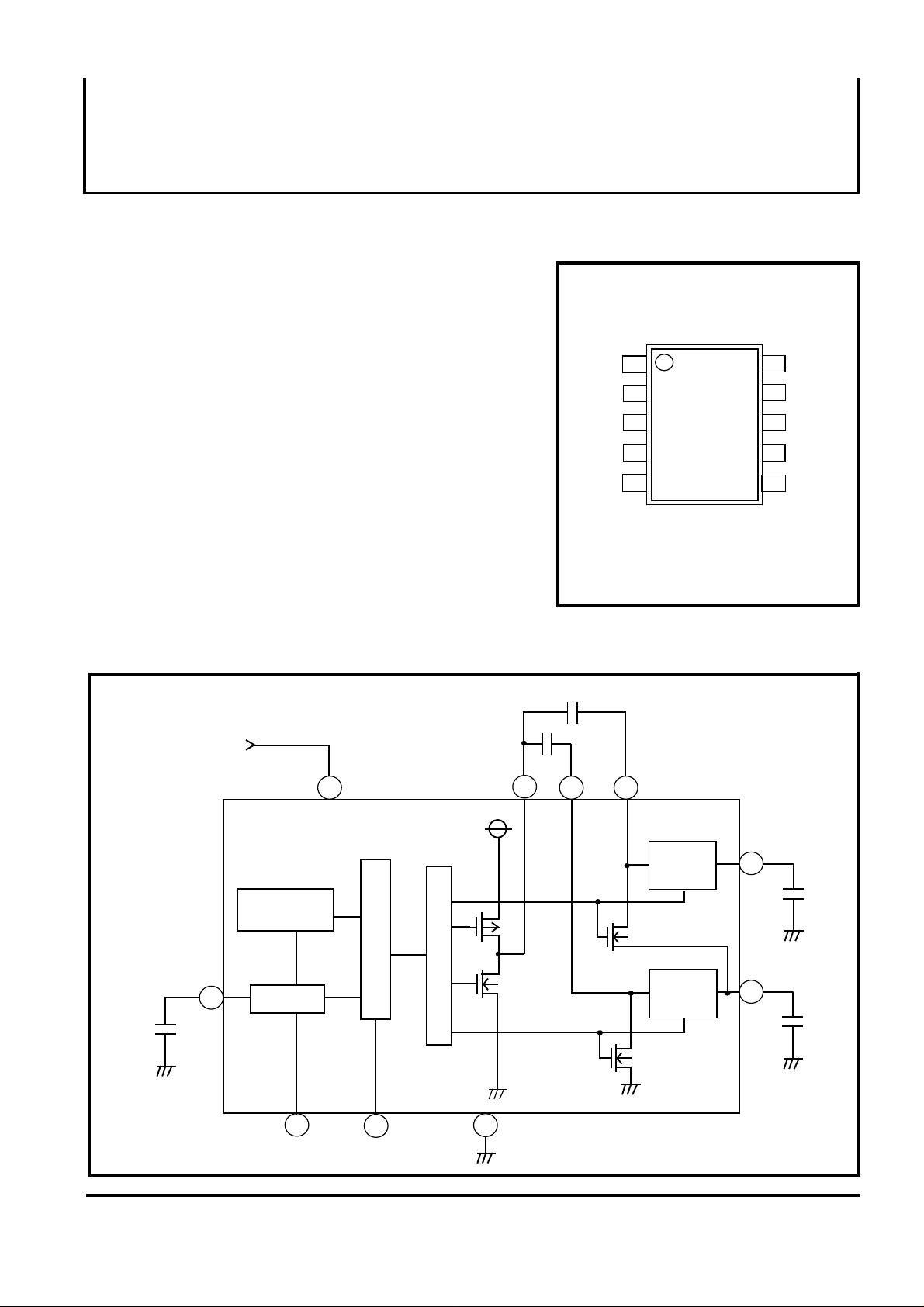
The M62262FP is a CMOS voltage converter for driving MMICs.
It includes a input inverter utilizing a charge-pump technique, therefore
it can provide both a just inverted output (-Vo) and a twice inverted
output (-2Vo) by connecting an external capacitor.
It can also switch over between a stand-by mode (a halt function with
low power dissipation) and a double clocking mode for reducing output
ripples.
FEATURE
• Availability of two outputs ; just inverted and twice inverted output
• Capability of output current ------- 30mA (min)
• Low voltage operation ------- Vin = 3V (typ)
• Low stand-by current (standby mode)
• Low out ripple (double clocking mode)
• Small 10-pin package
APPLICATION
• MMICs for a handy telephone and a PHS
M62262FP
VOLTAGE CONVERTER FOR MMIC
PIN CONFIGURATION(TOP VIEW)
COSC
VCC
CP1
GND
CP2
1
2
3
4
5
OUTLINE 10P2N
10 STB
9
8
-2VO
7
6
DCLK
-VO
CP3
BLOCK DIAGRAM
VCC=3V(typ)
COSC
1
VCC
Double clock
generator
Oscillator
STB
5
CP2
CP3
6
CHARGE
SW.
CHARGE
SW.
-2VO
7
-VO
8
CP1
2
Double clock selector
9
DCLK
Timing adjustment
3
410
GND
MITSUBISHI
( / 3 )
1

MITSUBISHI SEMICONDUCTORS<DIGI.ANA.INTERFACE>
PRELIMINALY
PRELIMINALY
Notices;This is not a final specification.
Some parametric limits are subject to change.
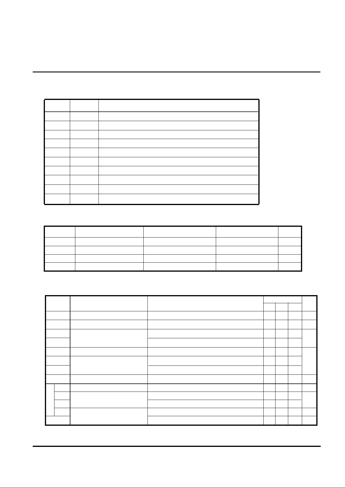
FUNCTION DESCRIPTION OF EACH PIN
PIN No. SYMBOL FUNCTION DESCRIPTION
1
2
3
4
5
6
7
8
9
COSC
VCC
CP1
GND
CP2
CP3
-2VO
-VO
DCLK
STB10
Connecting pin for capacitance of oscillator
Input voltage
Connecting pin 1 for a capacitor of charge-pump
GND pin
Connecting pin 2 for a capacitor of charge-pump
Connecting pin 3 for a capacitor of charge-pump
2-times inverted output
Just inverted output
Switchover between double cloking (H) and normal mode (L)
Switchover between stand-by (H) and actual operation (L)
ABSOLUTE MAXIMUM RATINGS(Ta=25°C unless otherwise noted)
M62262FP
VOLTAGE CONVERTER FOR MMIC
SYMBOL
VCC
PD
To p r
Ts t g
ELECTRICAL CHARACTERISTICS
SYMBOL
ICC
VCC
RO1
RO2
VEF
PEF2
fOSC COSC=220PF
DCLK
ISTB STB=VCC 2
Voltage conversion efficiency
ICC
RO1
RO2
fOSC
PARAMETER CONDITIONS
Supply voltage
Internal power dissipation
Operating temperture
Storage temperture
(VIN =3V, COSC=220PF, Ta=25°C, unless otherwise noted )
PARAMETER
Dissipation current
Range of sourse voltage
Output resistor
Power efficiency
Oscillating frequency
Dissipation current
Output resistor
Standby current
-Vout output pin (with load at -Vout pin only)
-2Vout output pin(with load at -2Vout pin only)
No load
-Vout output pin , IL=-5mA
-2Vout output pin , IL=-5mA
DCLK=VCC
-Vout output pin (with load at -Vout pin only)
-2Vout output pin(with load at -2Vout pin only)
COSC=220PF
CONDITIONS
RATINGS
6 V
440
- 20 ~ + 75
- 40 ~ +125
RATINGS
MIN TYP
450 900
30 60
90
99.8
95
90
90
6
2
0.6
20 40
60 120
12 20 kHz
4
UNIT
mW
°C
°C
MAX
180
5.52.7
10
UNIT
µA
V
Ω
%PEF1
kHz
mA
1
Ω
µA
5
MITSUBISHI
( / 3 )
2
 Loading...