MITSUBISHI SEMICONDUCTOR < STANDARD LINEAR IC >
GENERAL PURPOSE HIGH SPEED PWM CONTROL IC
GENERAL PURPOSE HIGH SPEED PWM CONTROL IC
DESCRIPTION
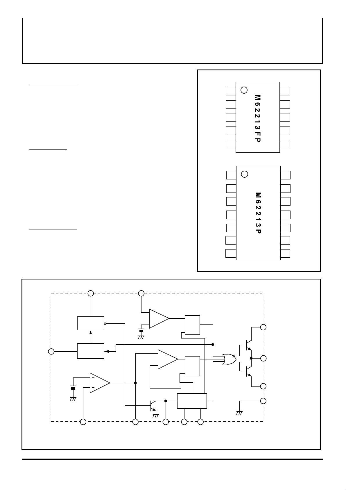
M62213P/FP is designed as a general purpose high-speed
PWM control IC.
This small 10 pin package contains many function and
protection circuits allowing simpler peripheral circuits and
compact set design.
This IC can operate high speed switching (700kHz Max)
with high speed PWM comparator and current limiting circuit.
FEATURES
• 700kHz operation to MOS- FET
• Output current Io= ±1A
• Totem pole output
• Timer type latch protection circuit with OVP
• Soft start operation is possible (with dead time control)
• Built-in OPAmp for feedback control
(photo coupler can be driven)
• High speed pulse-by-pulse current limiting
• Small size 10-pin SOP package
M62213P/FP
PIN CONFIGURATION (TOP VIEW)
RF
CF
1
2
3
4
5
OUTLINE 10P2N-A
1
2
3
4
VOUT
GND
CLM
VOUT
EMIT
GND
CLM
M62213P/FP
VCC
10
9
EA IN
8
EA OUT
7
SOFT
CT
6
COLLECT
14
VCC
13
12
EA IN
EA OUT
11
APPLICATION
• Switching Regulator
• DC-DC Converter
CT
(OVP)
2.5V
VCC CLM
UVLO
TIMER
LATCH
CLM
COMP
0.2V
PWM
COMP
S
CLM
LATCH
R
S
PWM
LATCH
R
RF
CF
N.C
5
6
7
OUTLINE 14P4
10
9
8
:note
COLLECT
VOUT
:note
EMIT
CT
SOFT
N.C
EA IN
EA OUT
(DTC)
( / 9 )
1
OSC.
GND
note: GND terminal is connected to emitter terminal
CFRFSOFT
as M6213FP in IC inside.
And Vcc terminal is connected to collector
terminal as M6213FP in IC inside.

MITSUBISHI SEMICONDUCTOR < STANDARD LINEAR IC >
M62213P/FP
GENERAL PURPOSE HIGH SPEED PWM CONTROL IC
ABSOLUTE MAXIMUM RATINGS (Ta=25°C, unless otherwise noted)
Symbol Parameter Condition Rating Unit
Vcc
IOUT
VCT
VEA IN
VCLM
Pd
Ktheta
Topr
Tstg
Supply voltage
Out terminal current
CT terminal supply voltage
EA IN terminal supply voltage
CLM terminal supply voltage
Power dissipation
Thermal derating
Operating temperature
Storage temperature
Continuous
Peak
Ta=25°C
Ta≥25°C
36
150
1.0
36
10
-0.3 ~ +4.0
440
3.52
-20 ~ +85
-40 ~ +150
V
mA
A
V
V
V
mW
mW/°C
°C
°C
ELECTRICAL CHARACTERISTICS (Ta=25°C, Vcc=14V, unless otherwise noted)
Limits
Block
CT
Symbol Parameter
Vcc
Vcc(START)
Vcc(STOP)
∆Vcc
IccL
Icco
IccOFF Timer latch circuit current
VTHCTH
VTHCTL
ICTDCHG
ICTCHG
VB
IB
AV
fT
IOS
Supply voltage range
Operation start-up voltage
Operation stop voltage
Start-up and stop
voltage difference
Stand-by current
Operating current
CT term. "H" threshold voltage
CT term. "L" threshold voltage
CT term. discherge current
CT term. cherge current
Reference voltage
Input bias current
Open loop gain
Unity gain bandwidth
Output source current
Test condition
Vcc=14V
Vcc=Vcc(STOP) + 0.2V
In normal operation
In CLM actuating
When VEAIN=0V
Typ Max
Vcc
(STOP)
Min
4.23.5
90
7.5
3.5 4.5
0.4
70
-33
180
13
4.0
0.7
100
-15
2.52.4 2.6
-300
-100
70
1
-100 -60-140
13.512.511.5
9.08.37.6
5.1
270
22
1.0
130
35
-5
Unit
V
V
V
V
µA
mA
mA0.9 2.0 3.00.9
mA1.8 2.70.8
V
V
µA
µA
V
0
nA
dB
MHz
µA
VOm + Output voltage (High)
VOm - Output voltage (Low)
( / 9 )
2
4.7 5.25 6.25
0 0.1 0.3
VV
V

MITSUBISHI SEMICONDUCTOR < STANDARD LINEAR IC >
M62213P/FP
GENERAL PURPOSE HIGH SPEED PWM CONTROL IC
ELECTRICAL CHARACTERISTICS (Ta=25°C, Vcc=14V, unless otherwise noted)
Block
C
L
M
S
O
F
T
OSC.
Symbol
VTHCLM
IOUTCLM
TPDCLM
VSOFT(0%)
VSOFT(50%)
Duty Max
ISOFT
fOSCmax
fOSC
VOL1
VOL2
VOH1
VOH2
TRISE
TFALL
Parameter
CLM term. threshold voltage
CLM term. output current
CLM term. delay time
Input voltage range at 0% duty
Input. voltage at 50% duty
Maximum duty
Soft term. input current
Maximum oscillation frequency
Oscillation frequency
Output low voltage
Output high voltage
Output voltage rise time
Output voltage fall time
Test condition
VCLM=0V
Delay time to output
Soft term. voltage range
to set 0% duty
Soft term. voltage at 50% duty
CF=270pF , RF=69 kΩ
Vcc=14V,Io=10mA
Vcc=14V,Io=100mA
Vcc=14V,Io=-10mA
Vcc=14V,Io=-100mA
No load
No load
Limits
Min
180
-270 -140
0 0.5
80
-65 -31
150 250
Typ Max
200
220
-200
90
2.7
90
99
-50
700
200
0.04 0.4
1.40.3
12.712.0
12.511.5
50
35
Unit
V
µA
nS
V
V
%
µA
KHz
KHz
V
V
V
V
nS
nS
( / 9 )
3
 Loading...