MITSUBISHI SEMICONDUCTORS <Standard Linear ICs>
DESCRIPTION
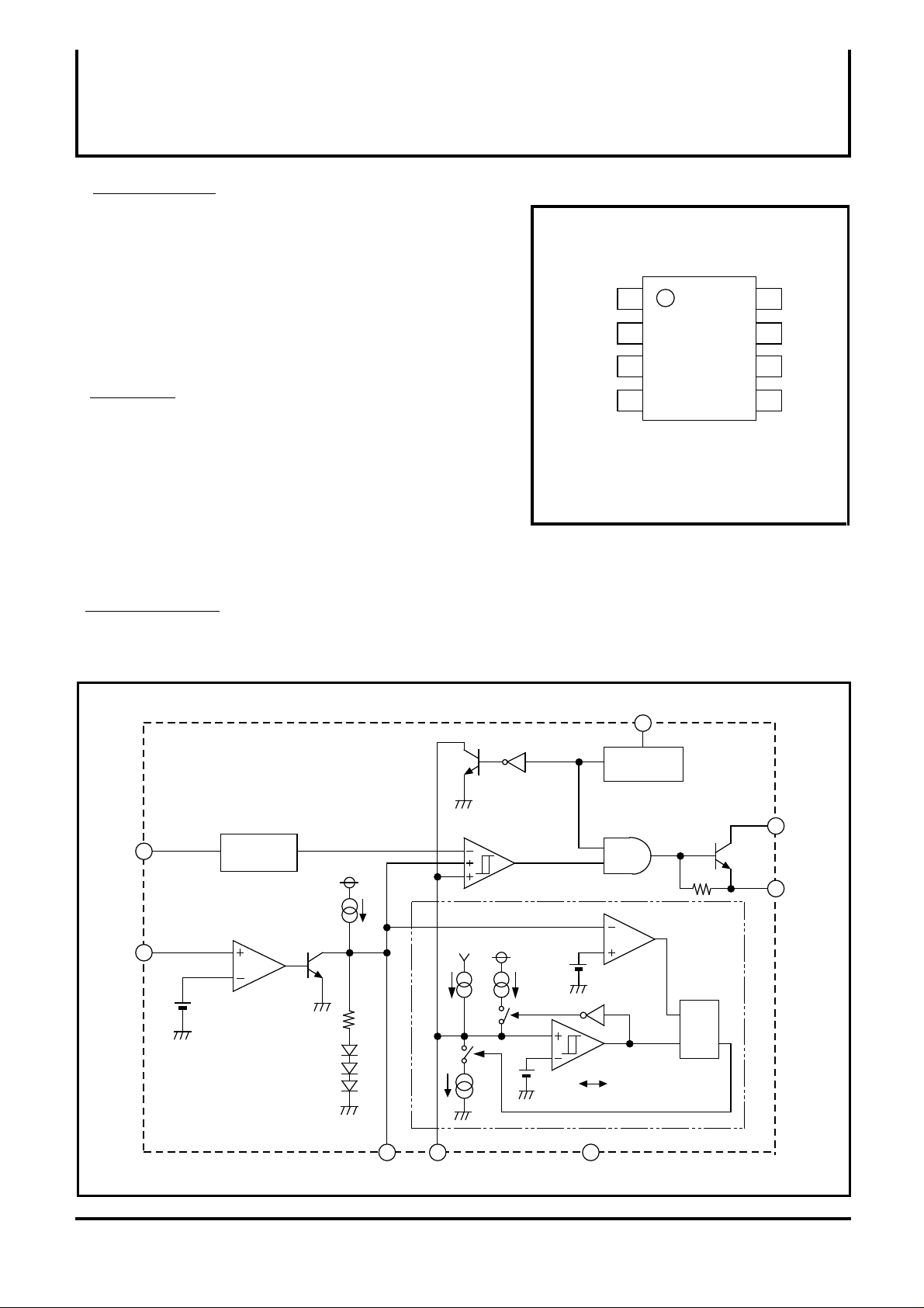
M62212 is designed as a general purpose DC-DC converter.
This small 8 pin package contains many functions allowing
simpler peripheral circuits and compact set design.
The output transistor is open collector and emitter follower
type. This makes the control STEP-UP,STEP-DOWN and
INVERTING converter.
FEATURE
• Wide operation power supply voltage range •••••••2.5 ~ 18V
• Low power consumption••••••••••••••••••••••••1.3mA typ
• High speed switching is possible.(300kHz)
• Output short protection circuit and ON/OFF control are used.
The dead-time control and the soft-start operation are
possible
• Package variation : 8pin DIP/SOP/SSOP8
M62212P/FP/GP
GENERAL PURPOSE DC-DC CONVERTER
PIN CONFIGURATION(TOP VIEW)
Collector
output
Emitter
output
GND
Cosc
1
2
3
4
OUTLINE 8P2S-A (FP)
8P2X (GP)
8P4 (P)
M62212P /
FP / GP
8
7
6
5
VCC
IN
FB
DTC
APPLICATIONS
General electric products, DC-DC converter
BLOCK DIAGRAM
COSC
IN
4
7
OSC
VCC
OP Amp
1.25V
1.25V
PWM Comp
VCC
VCC
8
U V L O
VTH : 2.3V
Short protection
circuit
1.86V
Collector
1
output
Emitter
2
output
R
Q
S
FB
6
5
DTC
( / 8 )
1
1.15V 0.3V
3
GND

MITSUBISHI SEMICONDUCTORS <Standard Linear ICs>
M62212P/FP/GP
GENERAL PURPOSE DC-DC CONVERTER
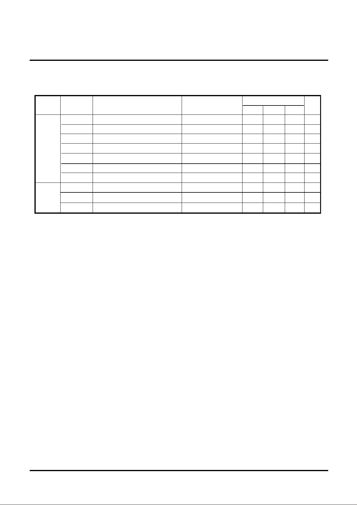
ABSOLUTE MAXIMUM RATINGS (Ta=25°C, unless otherwise noted)
Symbols Items Conditions Ratings Units
Vcc
Vo
Pd
Ktheta
Topr
Tstg
Power supply voltage
Output voltage
Output currentIo
Power dissipation
Thermal derating ratio
Operating ambient temperature
Storage temperature
Ta=25°C
Ta>25°C
19
19
150
625 (P) 360(FP) 250(GP)
5.00 (P) 2.88 (FP) 2.00(GP)
-20°C ~ +85
-40°C ~ +125
mW/°C
V
V
mA
mW
°C
°C
Electrical Characteristics ( Ta=25°C, Vcc =12V, Cosc=100pF unless otherwise noted )
Block
All
device
Std.
voltage
section
Error
amp.
section
Oscillator
section
UVLO
section
Symbol Items Test condition
VCC
I CC ST
V REF
L INE
I B
A V
G B
+
VOM
-
VOM
+
I OM
-
I OM
f OSC
VOSCH
VOSCL
I OSC CH
I OSC DIS1
VTH ON
VTH OFF
VHYS Hysteresis
Range of power supply voltage
Standby current
Standard voltage
Line regulation
Input bias current
Open loop gain
Unity gain bandwidth
Output high voltage
Output low voltage
Output sink current
Output source current
Oscillation frequency
Upper limit voltage of oscillation waveform
Lower limit voltage of oscillation waveform
Cosc charge current
Cosc discharge current 1
Start-up threshold voltage
Shut-down threshold voltage
Output "OFF" status
Voltage follower
VCC=2.5 ~ 18V
VFB=1.86V
VIN =1V
VIN =1V 2.3
VIN =1V
VHYS = VTHON - VTHOFF
Min Typ Max
2.5 18
1.19 1.25 1.31
1.82 2.62
2.2 2.4
20 80
Limits
1.3 1.8
5 12
80
0.6
6
-60 -30
110
1.0
0.45
-40
10
2.25
50
500
400
Units
V
mA
V
mV
nA
dB
MHz
V
mV
mA
uA
kHz
V
V
uA
uA
V
V
mV
( / 8 )
2

MITSUBISHI SEMICONDUCTORS <Standard Linear ICs>
M62212P/FP/GP
GENERAL PURPOSE DC-DC CONVERTER
Electrical Characteristics ( Ta=25°C, Vcc =12V, Cosc=100pF unless otherwise noted )
Block
Short
protection
circuit
Output
section
Symbol
VTH FB
VTH DTC
VTL DTC
I CH1
I DIS1
I CH2
I DIS2
I CL
VSAT1
VSAT2
Items Test condition
FB threshold voltage
Latch mode "H" threshold voltage
Latch mode "L" threshold voltage
DTC charge current when start-up
DTC discharge current 1
DTC charge current when stable state
DTC discharge current 2
Collector output leak current
Collector output saturation voltage 1
Collector output saturation voltage 2
VIN =1V,VDTC=0.7V
VIN =1V,VFB =2.11V
VIN =1V,VFB =2.11V
VDTC=0.7V,VFB =2.11V
VDTC=0.7V,VFB =2.11V
VDTC=0.7V,VFB = 0.7V
VDTC=0.2V,VFB =2.11V
VCE=18V , VCC=18V
Emitter GND,
IC=150mA,VE=0V
Emitter follower,
IE=50mA,VC=12V
Limits
Min Typ Max
1.86
1.15
0.3
-45
50
-10
15
-1 1
0.3
1.6
1.1
Units
V
V
V
µA
µA
µA
µA
µA
V
V
( / 8 )
3
 Loading...