Mitsubishi M62210FP Datasheet

MITSUBISHI SEMICONDUCTORS <DIGI•ANA INTERFACE>
GENERAL PURPOSE MULTI FUNCTION DC-DC CONVERTER
DESCRIPTION
M62210FP is designed as a general purpose multi-function
DC-DC converter. This is most suitable as a back-light control
for a LCD,etc.
This small 10 pin package contains many functions allowing
simpler peripheral circuits and compact set design.
The input of this unit has two channels containing priority
control circuit. This makes the control a simple matter when
the back-light is on and during the stable state.
FEATURE
Wide operation power supply voltage range…………2.5~18V
Low power consumption ………………………………1.3mA typ
Operation can be synchronized by the external sync signal
Operation can be controlled using two prioritized systems.
(High input has priority)
High speed switching is possible.(300kHz)
Output short protection circuit and ON/OFF control are used.
The dead-time control and the soft-start operation are
possible
Small size 10-pin SOP package.
APPLICATIONS
Back-light control of personal computers and word processors
General electric products
M62210FP
Notice: This is not a final specification.
Some parametric limits are subject to change.
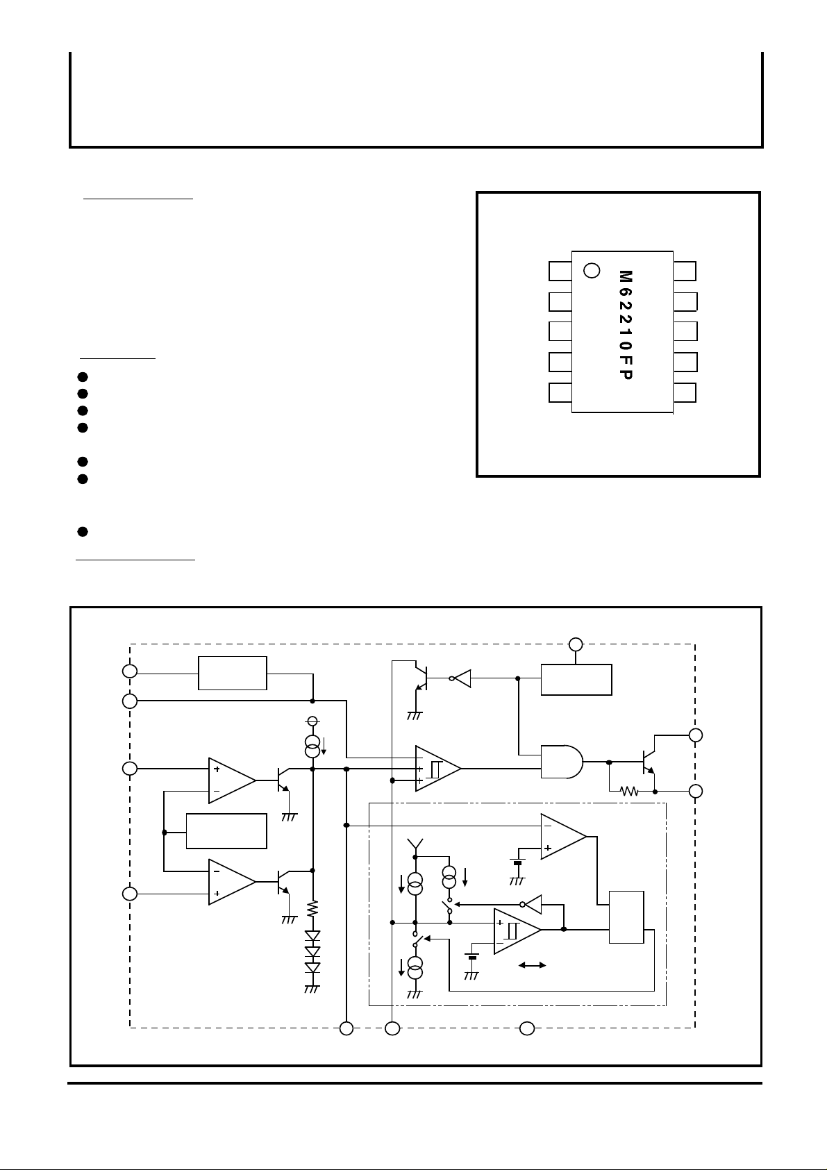
PIN CONFIGURATION(TOP VIEW)
Collector
output
Emitter
output
GND
COSC
TIN
1
2
3
4
5
OUTLINE 10P2
10
VCC
9
IN1
8
IN2
FB
7
6
DTC
BLOCK DIAGRAM
5
TIN
COSC
4
OP Amp1
IN1
9
Std. voltage
IN2
8
OP Amp2
OSC &
sync ckt
1.25V
VCC
FB
VCC
10
U V L O
V TH : 2.3V
Collector
1
2
output
Emitter
output
PWM Comp
Short protection
1.25V
circuit
R
S
Q
1.25V
1.15V 0.3V
7
6
DTC
3
GND
( 1 / 9 )

MITSUBISHI SEMICONDUCTORS <DIGI•ANA INTERFACE>
GENERAL PURPOSE MULTI FUNCTION DC-DC CONVERTER
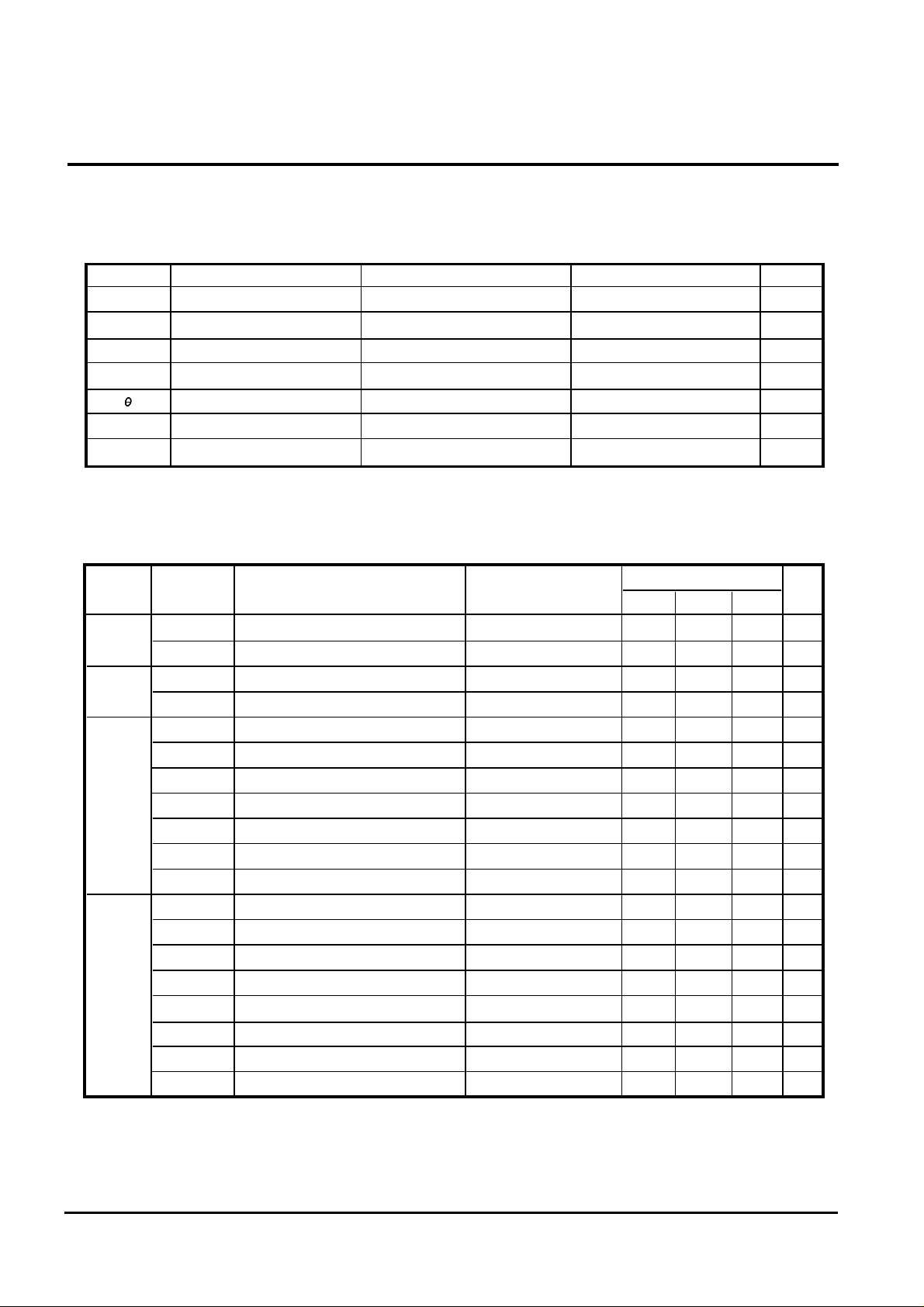
ABSOLUTE MAXIMUM RATINGS (Ta=25ºC unless otherwise noted)
M62210FP
Symbols Items
Vcc
Vo
Io
Pd
K
Topr
Tstg
Power supply voltage
Output voltage
Output current
Power dissipation
Thermal derating ratio
Operating ambient temperature
Storage temperature
Conditions
Ta=25ºC
Ta>25ºC
Ratings Units
19
19
150
360
2.88
-20ºC~+85
-40ºC~+125
Electrical Characteristics ( Ta=25ºC, Vcc =12V, Cosc=100pF unless otherwise noted )
Block
All
device
Std.
voltage
section
Error
amp.
section
Oscillator
section
Symbol Items Test condition Units
VCC
I CC ST
V REF
L INE
I B
A V
G B
+
VOM
-
VOM
+
I OM
-
I OM
f OSC
VOSCH
VOSCL
I OSC CH
I OSC DIS1
I OSC DIS2
VTINH
VTINL
Range of power supply voltage
Standby current
Standard voltage
Line regulation
Input bias current
Open loop gain
Unity gain bandwidth
Output high voltage
Output low voltage
Output sink current
Output source current
Oscillation frequency
Upper limit voltage of oscillation waveform
Lower limit voltage of oscillation waveform
Cosc charge current
Cosc discharge current 1
Cosc discharge current 2
TIN "H" level
TIN "L" level V
Output "OFF" status
Voltage follower
VCC=2.5~18V
VFB=1.25V
VIN1=1V , VIN2=1V
Min Typ Max
2.5 18
1.19 1.25 1.31
1.7 2.5
2.2
Limits
1.3 1.8
5 12
80
0.6
6
-60 -30
110
1.0
0.45
-40
10
40
500
400
V
CC
1.0
V
V
mA
mW
mW/ºC
ºC
ºC
V
mA
V
mV
nA
dB
MHz
V
mV
mA
uA
kHz
V
V
uA
uA
uA
V
( 2 / 9 )

MITSUBISHI SEMICONDUCTORS <DIGI•ANA INTERFACE>
GENERAL PURPOSE MULTI FUNCTION DC-DC CONVERTER
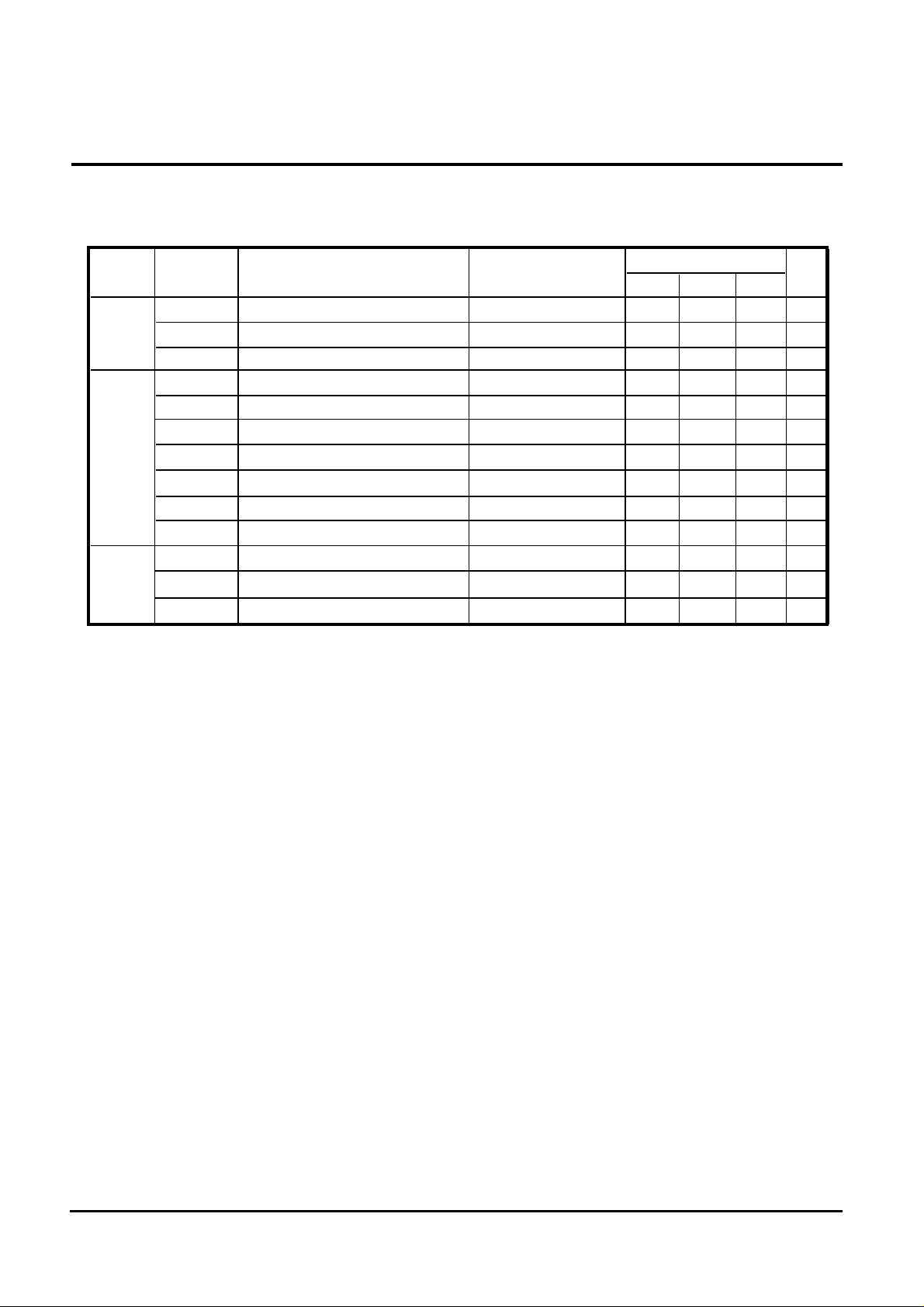
Electrical Characteristics ( Ta=25ºC, Vcc =12V, Cosc=100pF unless otherwise noted )
M62210FP
Block
UVLO
section
Short
protec
tion
circuit
Output
section
Symbol
VTH ON
VTH OFF
VHYS
VTH FB
VTH DTC
VTL DTC
I CH1
I DIS1
I CH2
I DIS2
I CL
VSAT1
VSAT2
Items Test condition
Start-up threshold voltage
Shut-down threshold voltage
Hysteresis
FB threshold voltage
Latch mode "H" threshold voltage
Latch mode "L" threshold voltage
DTC charge current when start-up
DTC discharge current 1
DTC charge current when stable state
DTC discharge current 2
Collector output leak current
Collector output saturation voltage 1
Collector output saturation voltage 2
VIN1=1V , VIN2=1V
VIN1=1V , VIN2=1V
VHYS = VTHON - VTHOFF
VIN1=1V,VIN2=1V,VDTC=0.7V
VIN1=1V,VIN2=1V,VFB =1.5V
VIN1=1V,VIN2=1V,VFB =1.5V
VDTC=0.7V,VFB =1.5V
VDTC=0.7V,VFB =1.5V
VDTC=0.7V,VFB = 0.7V
VDTC=0.2V,VFB =1.5V
VCE=18V , VCC=18V
Emitter GND,
IC=150mA,VE=0V
Emitter follower,
IE=50mA,VC=12V
Limits
Min Typ Max
2.2 2.4
20
-1 1
2.3
2.25
50
1.25
1.15
0.3
-45
50
-10
15
0.3
1.6
80
1.1
Units
V
V
mV
V
V
V
µA
µA
µA
µA
µA
V
V
( 3 / 9 )
 Loading...