Mitsubishi M62030FP Datasheet

VOLTAGE DETECTING, SYSTEM RESETTING IC SERIES
GENERAL DESCRIPTION
The M62030FP is a voltage threshold detector designed for
detection of an input voltage/supply voltage and generation of
a system reset pulse for almost all logic circuits such as
microcontroller.
It contains a delay circuit which provides 200µs (typ) delay
and 4 modes of delays [25ms, 50ms, 100ms, 200ms (typ)] in
the input voltage detection type and in the supply voltage
detection type, respectively.
FEATURES
• Built-in 2 functional circuits for detecting voltage
• Built-in delay circuit to provide long delay time
(without external delay capacitors)
• Selectable 4 modes of delay time
[25msec, 50msec, 100msec, 200msec(typ)]
• Few external components
• Small 8-pin SOP package
MITSUBISHI<Dig./Ana. INTERFACE>
M62030FP
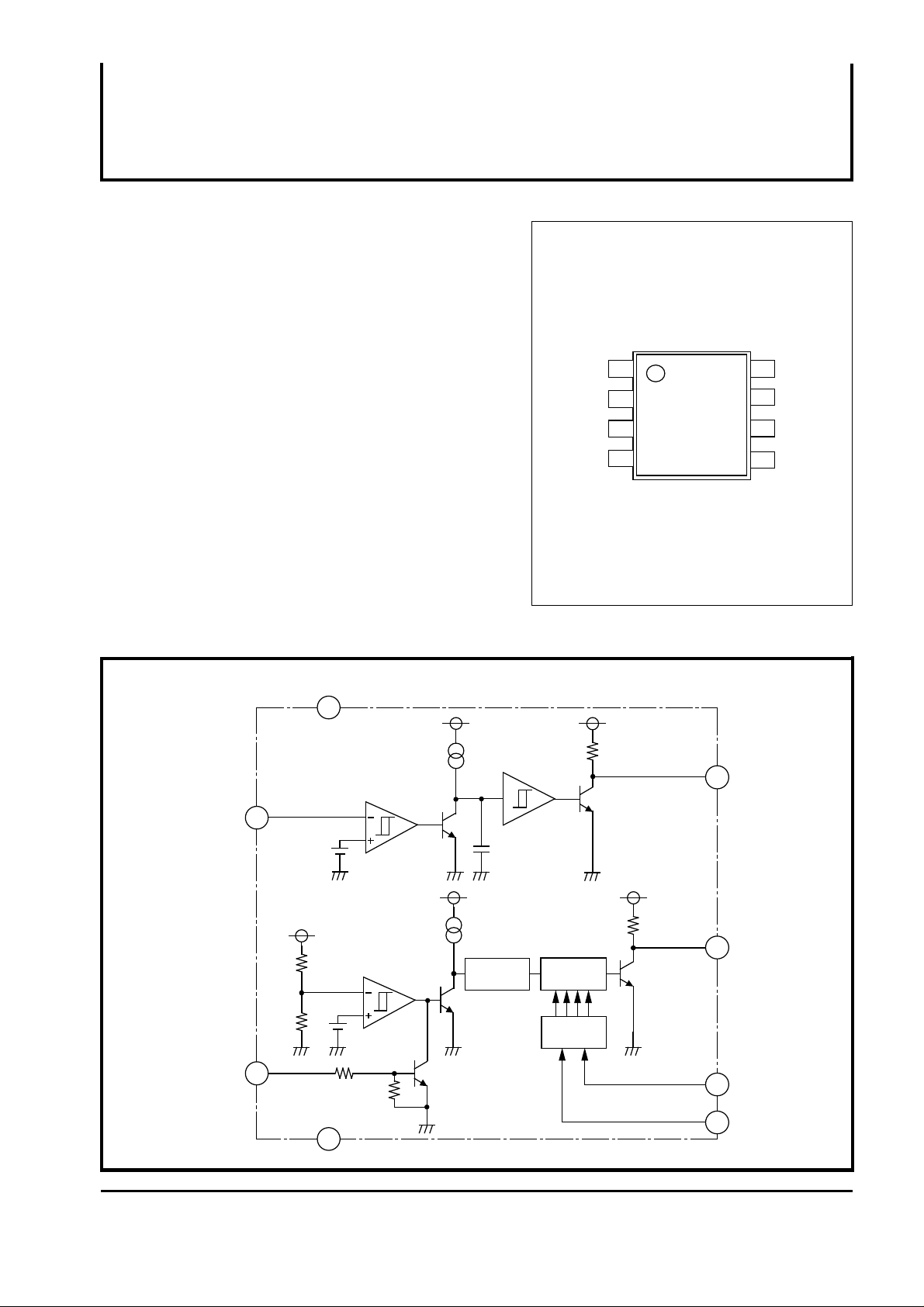
PIN CONFIGURATION (TOP VIEW)
1 VRES
Ct0
VIN
2
Ct1
3
GND
4
M62030FP
8
7
6
5
Vcc
OUT1
OUT2
APPLICATION
• Reset circuits of MCU, MPU and logics
RECOMMEND OPERATING CONDITION
• Supply voltage range ………… 2V to 10V
BLOCK DIAGRAM
Vcc
7
VIN
2
1.25V
Vcc
Vcc
OSCILLATOR
FREQUENCY
DIVIDER
Outline 8P2S-A
Vcc
VccVcc
6
OUT1
OUT2
5
VRES
1.25V
8
MULTIPLEXER
3
Ct1
1
Ct0
4
GND
1
( / 5 )

MITSUBISHI<Dig./Ana. INTERFACE>
M62030FP
VOLTAGE DETECTING, SYSTEM RESETTING IC SERIES
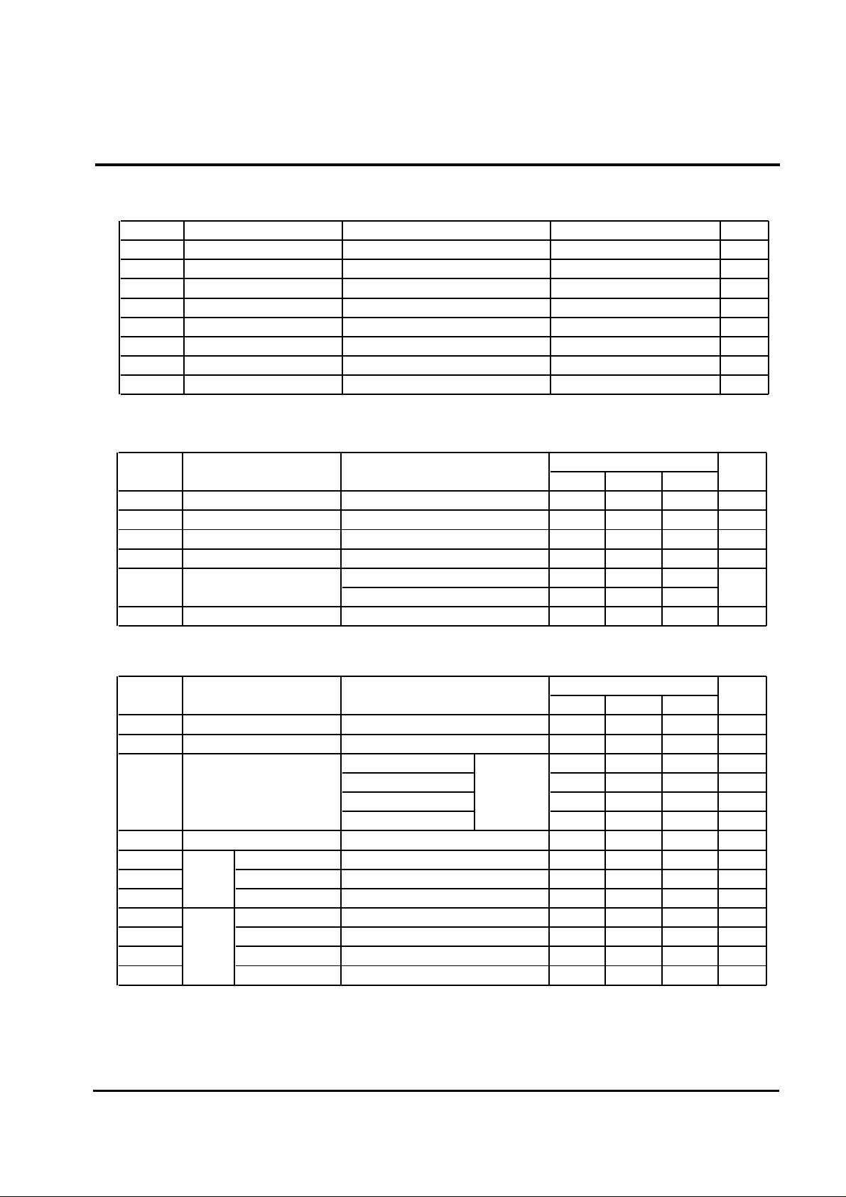
ABSOLUTE MAXIMUM RATINGS (Ta=25°C, unless otherwise noted)
Symbol Parameter Conditions Ratings Unit
Vcc Supply voltage V
ISINK1,2 Output Sink Current Output1,2 8.0 mA
VO Output voltage V
VRES V
Self reset input voltage
Pd Power dissipation 300 mW
Ktheta Thermal Derating 3.0 mW/°C
Ta ≥ 25°C
Topr Operating temperature
Tstg Storage temperature
ELECTRICAL CHARACTERISTICS (Ta = -20 to 75°C, unless otherwise noted)
< Reset circuit 1 >
Symbol Parameter Test Conditions
VS1 Detecting voltage 1 Ta= 25°C 1.20 1.25 1.30 V
∆Vs1
TPLH1 CL=100pF,Ta= 25°C 80 200 500
VOL1 VIN<1.2V, IOL=5mA, Vcc=5V 0.2 0.4 V
VIN
Hysteresis voltage 1
Output "L to H" propagation delay time 1
Low output voltage 1
Input voltage
Ta= 25°C 9 15 23 mV
Vcc ≤ 7V
Vcc > 7V
IIN Input Current VIN=1.25V 100 500 nA
-0.3 to 10
-0.3 to 10
-0.3 to 10
-20 to 75 °C
-40 to 125
Limits
Min Typ Max
-0.3 Vcc
-0.3 7.0
°C
Unit
µs
V
< Reset circuit 2 >
Symbol Parameter Test Conditions
S2 Detecting voltage 2
V
Ta= 25°C 4.0 4.2 4.4 V
Min Typ Max
Limits
Unit
∆ VS2 Hysteresis voltage 2 Ta= 25°C 30 50 100 mV
Ct0 ="L", Ct1="H"
T
PLH2
VOL2
VRESH Input High voltage 2 Vcc V
IRESH Input High current VRES=2V 80
Output "L to H" propagation delay time 2
Low output voltage 2
Self
Reset
VRESL Input Low voltage -0.3 0.8 V
VCt0,1H Input High voltage 1.4 V
VCt0,1L Input Low voltage 0.6 V
ICt0,1H Input High current 75
Ct0
Ct1
ICt0,1L Input Low current 75
Ct0 ="H", Ct1="L"
Ct0 ="H", Ct1="H" or opening
Ct0="L",Ct1="L"
CL=100pF 50 ms
Ta= 25°C 100 ms
Vcc=4.0V,IOL=5mA 0.2 0.4 V
Ta= 25°C
Ta= 25°C
Ta= 25°C
Ta= 25°C
Ta= 25°C
Ta= 25°C
Ta= 25°C
25 ms
200 ms
µA
µA
µA
2
( / 5 )
 Loading...