

PRELIMINARY
PRELIMINARY
Notice:This is not a final specification.
Some parametric limits are subject to change.
MITSUBISHI <Dig./Ana.INTERFACE>
M62023L,P,FP
SYSTEM RESET IC WITH SWITCH FOR MEMORY BACK-UP
GENERAL DESCRIPTION
The M62023L/P/FP is a system reset IC that controls the memory
backup function of an SRAM and an embedded RAM of a
microcontroller.
The IC outputs reset signals (RES/RES) to a microcontroller at
power-down and power failure. It also shifts the power supply to
RAMs from main to backup, outputs a signal (CS) that invokes
standby mode, and alters RAMs to backup circuit mode.
FEATURES
• Built-in switch for selection between main power supply and back up power supply to RAMs
• Small difference between input and output voltages
(IOUT=80mA, VIN=3V) : 0.15V typ
• Detection voltage (power supply monitor voltage) : 2.57V typ
• Chip select signal output (CS)
• Two channels of reset outputs (RES/RES)
• Power on reset circuit
APPLICATION
Power supply control systems for memory of microcontroller
systems in electronic equipment such as OA equipment,
industrial equipment, and home-use electronic appliances
and SRAM boards with built-in backup function that require
switching between external power supply and battery.
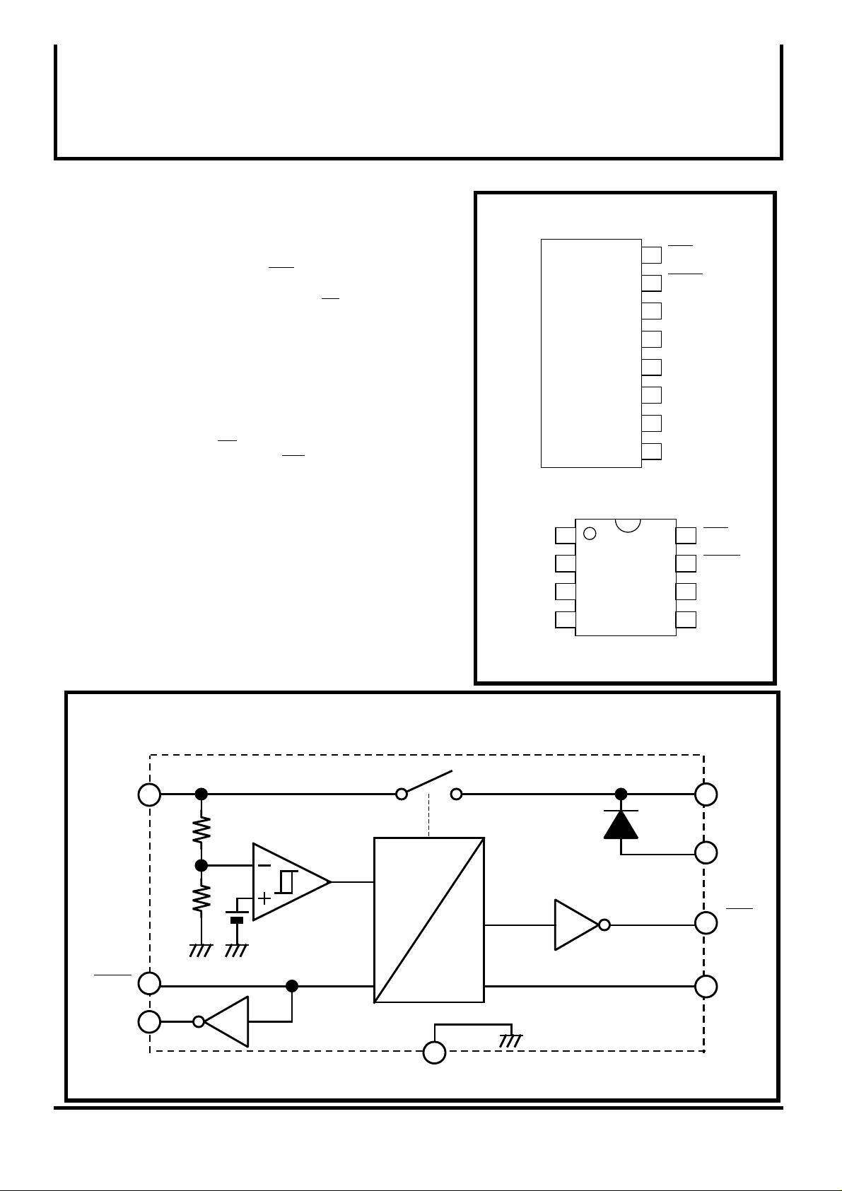
PIN CONFIGURATION (TOP VIEW)
8 CS
7 RES
6 GND
5 RES
4 Ct
3 VIN
2 VBAT
1 VOUT
Outline 8P5 (L)
VOUT 1
VBAT 2
VIN 3
8 CS
7 RES
6 GND
BLOCK DIAGRAM
VIN
3
R1
R2
RES
RES
7
5
Com
1.24V
SW
RESET
CIRCUIT
DELAY
CIRCUIT
Ct 4
Outline 8P4 (P)
8P2S-A (FP)
D1
5 RES
1
VOUT
VBAT
2
CS
8
4
Ct
6
GND
( / )
1 4
1997.5.30- rev
MITSUBISHI <Dig./Ana.INTERFACE>
M62023L,P,FP
PRELIMINARY
PRELIMINARY
Notice:This is not a final specification.
Some parametric limits are subject to change.
ABSOLUTE MAXIMUM RATINGS (Ta=25°C, unless otherwise noted)
Symbol Parameter Conditions Ratings Unit
VIN
IOUT
Input voltage
Output current
Pd Power dissipation 800(L)/625(P)/440(FP) mW
K
Topr
Tstg
Thermal derating mW/°C
Operating temperature
Storage temperature
ELECTRICAL CHARACTERISTICS (Ta=25°C, unless otherwise noted)
SYSTEM RESET IC WITH SWITCH FOR MEMORY BACK-UP
7
100
Ta ≥ 25°C
8(L)/6.25(P)/4.4(FP)
-20 to +75
-40 to +125
V
mA
°C
°C
Symbol Parameter Unit
VS 2.44 V
∆VS
ICC Circuit current
Detection voltage
Hysteresis voltage mV
VIN (At charge from H L)
∆VS=VSH-VSL
IOUT=0mA
Test Conditions
VIN=2V
VIN=3V
VDROP
VOH(Ct)
VOL(Ct)
VOH(RES)
VOL(RES)
VOH(RES)
VOL(RES)
VOH(CS)
VOL(CS)
IR
VF
tpd
td
VOPL(RES)
Difference between
input and output voltages
Ct output voltage (high level)
Ct output voltage (low level)
RES output voltage (high level)
RES output voltage (low level)
RES output voltage (high level)
RES output voltage (low level)
CS output voltage (high level)
CS output voltage (low level)
Backup Di leak current
Backup Di forward direction voltage
Delay time
Response time
RES limit voltage of operation
VIN=3V
VIN=3V (Note 1)
VIN=2V (Note 1)
VIN=2V (Note 1)
VIN=3V
VIN=3V (Note 1)
VIN=2V
VIN=2V (Note 2)
VIN=0V, VBAT=3V (Note 2)
VIN=3V
VBAT=3V
IF=10µA
VIN=0V 3V, Ct=4.7µF
VIN=3V 2V
(Note 3)
IOUT=50mA
IOUT=80mA
(Note 1)
Isink=1mA
(Note 1)
Isink=1mA
(Note 1)
Isink=1mA
VIN=3V
VIN=0V
Limits
Min Typ Max
2.57
2.70
50 200100
1.5 3.0
6.5
10
0.1 0.2
0.15 0.3
2.42.0
0.02 0.1
2.01.5
0.02
0.04 0.2
3.02.5
0.02
0.04 0.2
1.61.3
2.472.40
0.07
0.08 0.3
±0.5
±0.5
0.54 0.6
27 5510
5.0 25.0
0.65
mA
V
V
V
V
V
V
V
V
V
µA
V
ms
µs
V
Note 1. Regarding conditions to measure VOH and VOL, voltage values are generated by internal resistance only and no external
resistor is used.
2. These values are produced inserting an external resistor, RCS=1MΩ, between the CS pin and GND.
3. With no external resistor (10KΩ internal resistance only)
( / )
2 4
1997.5.30- rev
PRELIMINARY
PRELIMINARY
Notice:This is not a final specification.
Some parametric limits are subject to change.
SYSTEM RESET IC WITH SWITCH FOR MEMORY BACK-UP
EXPLANATION OF TERMINALS
MITSUBISHI <Dig./Ana.INTERFACE>
M62023L,P,FP
Pin No. Name Function
Symbol
VIN and VBAT are controlled by means of an internal switch and output through
VOUT.
The pin is capable of outputting up to 100 mA. Use it as VDD of CMOS RAM
and the like.
Backup power supply is connected to this pin.
If a lithium battery is used, insert a resistor in series for safety purposes.
+3V input pin. Connect to a logic power supply.
A delay capacitor is connected to this pin. By connecting a capacitor, it is
possible to delay each output.
Connect to the positive reset input of a microcontroller. The pin is capable of
flowing 1mA sink current.
Reference for all signals
Connect to the negative reset input of a microcontroller. The pin is capable of
flowing 1mA sink current.
Connect to the chip select of RAM. The CS output is at low level in normal state
thereby letting RAM be active. Under failure or backup condition, the CS
output is set to high level, then RAM enters standby state disabling read/write
function. The pin is capable of flowing a 1mA sink current.
Ct
CS
Power supply output
Backup power supply
input
Power supply input
Delay capacitor
connection pin
Positive reset output
Ground
Negative reset output
Chip select output
1
VOUT
2
3
VBAT
VIN
4
5
6
7
RES
GND
RES
8
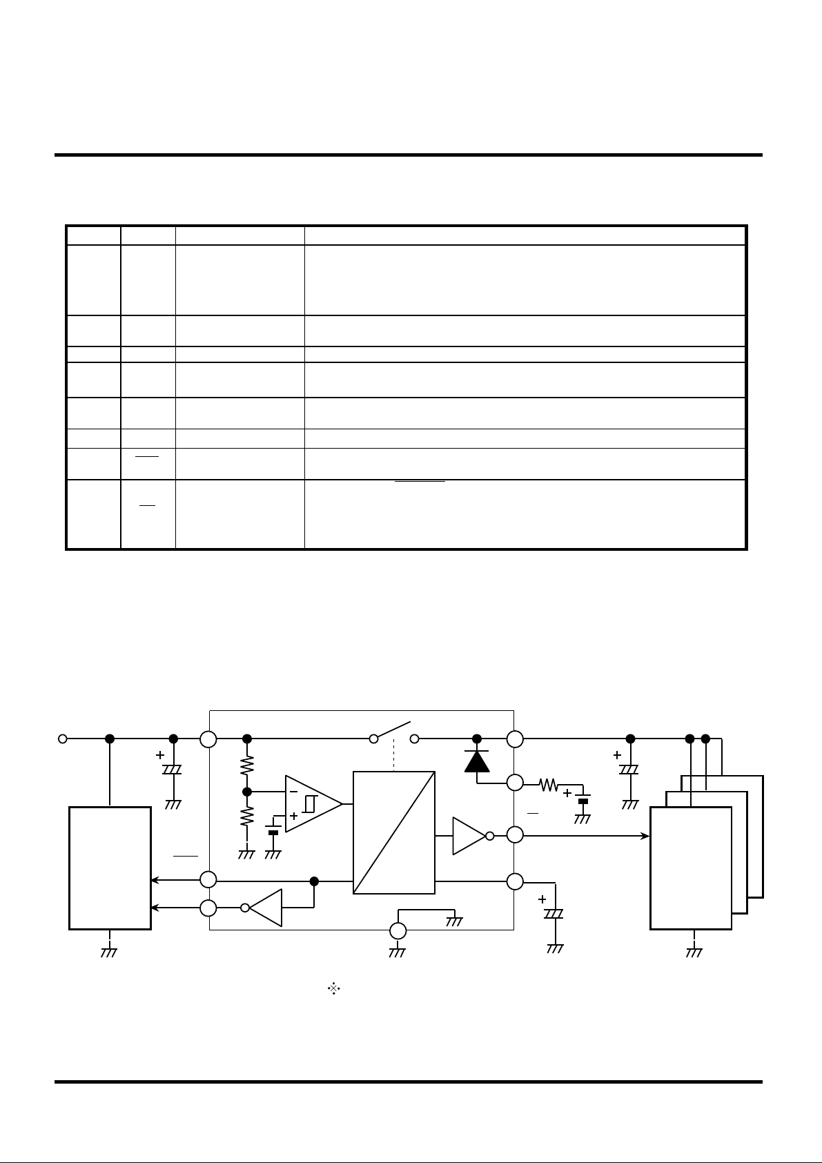
APPLICATION EXAMPLE
+3V
(MAIN POWER SUPPLY)
CIN
VDD
MCU
or
CPU
VIN
RES
RES
M62023
1
2
8
4
VOUT
VBAT
CS
Ct
BATTERY
3V
Ct
COUT
VDD
CMOS
RAM
SW
3
R1
R2
7
5
Com
RESET
CIRCUIT
1.24V
DELAY
CIRCUIT
GND
D1
6
Capacitance to be connected: CIN: 10µF; COUT: 4.7µF; Ct: 4.7µF
( / )
3 4
1997.5.30- rev

PRELIMINARY
PRELIMINARY
Notice:This is not a final specification.
Some parametric limits are subject to change.
MITSUBISHI <Dig./Ana.INTERFACE>
M62023L,P,FP
SYSTEM RESET IC WITH SWITCH FOR MEMORY BACK-UP
TIMING CHART
VIN
0V
VOUT
CS
RES
3V
tpd tpd
V1
V2
VSH
VSL
∆VS
V3
V2
V3
VOL(CS)
3V
VIN(VSL)
Input
voltage
Output
pin
VOUT
RES
RES
RES
In normal operation
Input voltage : 3V
With SW Tr. set to ON, a
voltage (VIN-VDROP) is output
The output level is VOL(RES)
with a logic low
The output level is VOH(RES)
with a logic high
In failure
(instantaneous drop)
Input voltage : 3V 2V
Each output varies if the input
voltage drops to VSL or under
SW Tr. is turned OFF. A
voltage (VIN-VEB) is output by
the diode between E and B of
SW Tr.
As the state shifts from a logic
low to logic high, the output
level becomes approximately
equal to the input voltage
As the state shifts from a logic
high to logic low, the output
level becomes VOL(RES)
Restoration from failure
(instantaneous drop)
Input voltage : 2V 3V
If the input voltage goes higher
than VSL by 100mV, each
output varies after delay
produced by the delay circuit
SW Tr. is turned ON after delay
and a voltage (VIN-VDROP) is
output
A logic high is maintained, and
then shifts to a logic low
A logic low is maintained, and
then shifts to a logic high
VOL(RES)
VOH(RES)
VIN(VSL)
VOL(RES)
V1=VIN-VDROP
V2=VIN-VEB(SW Tr.)
V3=VBAT-VF
In backup state
Input voltage : 0V
Backup voltage : 3V
VBAT-VF
The output level is VOL(CS)
with a logic low
CS
As the state shifts from a logic
low to logic high, the output
level becomes the voltage
VIN-VEB
( / )
4 4
A logic high is maintained, and
then shifts to a logic low
The output is a logic high and
the output level is VBAT-VF
1997.5.30- rev
 Loading...