Mitsubishi M62022FP Datasheet

MITSUBISHI<Dig.Ana.INTERFACE>
battery check,level detection and waveform shaping.
Overvoltage protection circuit.
Supply voltage range......................2~17V
M62022L,FP
VOLTAGE DETECTING,SYSTEM RESETTING IC
DESCRIPTION
The M62022 is a semiconductor integrated circuit resets logic
circuits according to supply voltage.It is used with many types
of circuits,including central processing units.
With the built-in delay circuit,delay time can be adjusted at
the user’s option by externally adding capacitance.
This circuit can also be used in other applications,such as
FEATURES
•Requires only a few external components.
•Ensures long delay time at low capacitance.
e.g.Delay time is 100ms at 0.33µF.
•Limit operating voltage*is low.
0.6V standard(Resistance RL=22kΩ)
(*Minimum supply voltage at which output can be kept low.)
•Wide supply voltage range.....................2~17V
•Highly resistant to rapid voltage fluctuation
•Wide application range
•5-pin single in-line package equivalent in height to dual in-line
package
APPLICATION
Reset circuit in p-channel metal-oxide semiconductors,n-
channel metal-oxide semiconductors,complementary
metal-oxide semiconductors,microcomputers,central
processing units,microcomputer units and other logic
circuits,Battery check circuit,Backup power selection
circuit;Level detection circuit,Waveform shaping circuit,
Delay waveform generation circuit,DC-DC converter,and
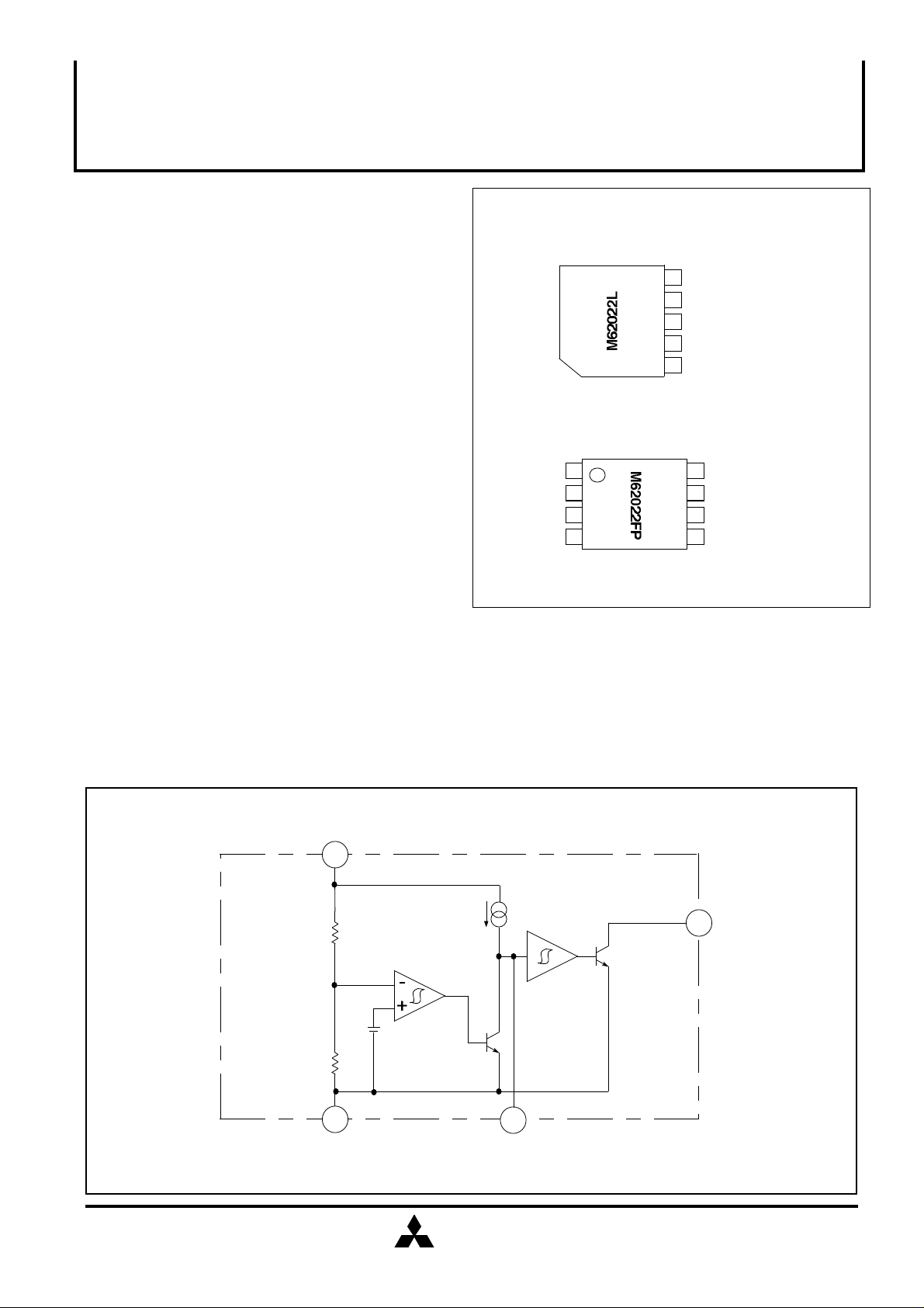
PIN CONFIGURATION (TOP VIEW)
5
OUTPUT
4
DELAY CAPACITANCE
3
GND
2
NC
POWER SUPPLY
1
Outline 5P5T
NC
NC
NC
GND
1
2
3
4
Outline 8P2S-A
8
NC
7
POWER SUPPLY
6
OUTPUT
5
DELAY CAPACITANCE
NC:NO CONNECTION
RECOMMENDED OPERATING VOLTAGE
BLOCK DIAGRAM
POWER SUPPLY
R1
R2
GND
5µA
(STANDARD)
OUTPUT
DELAY CAPACITANCE
MITSUBISHI
ELECTRIC
1
( / 2 )

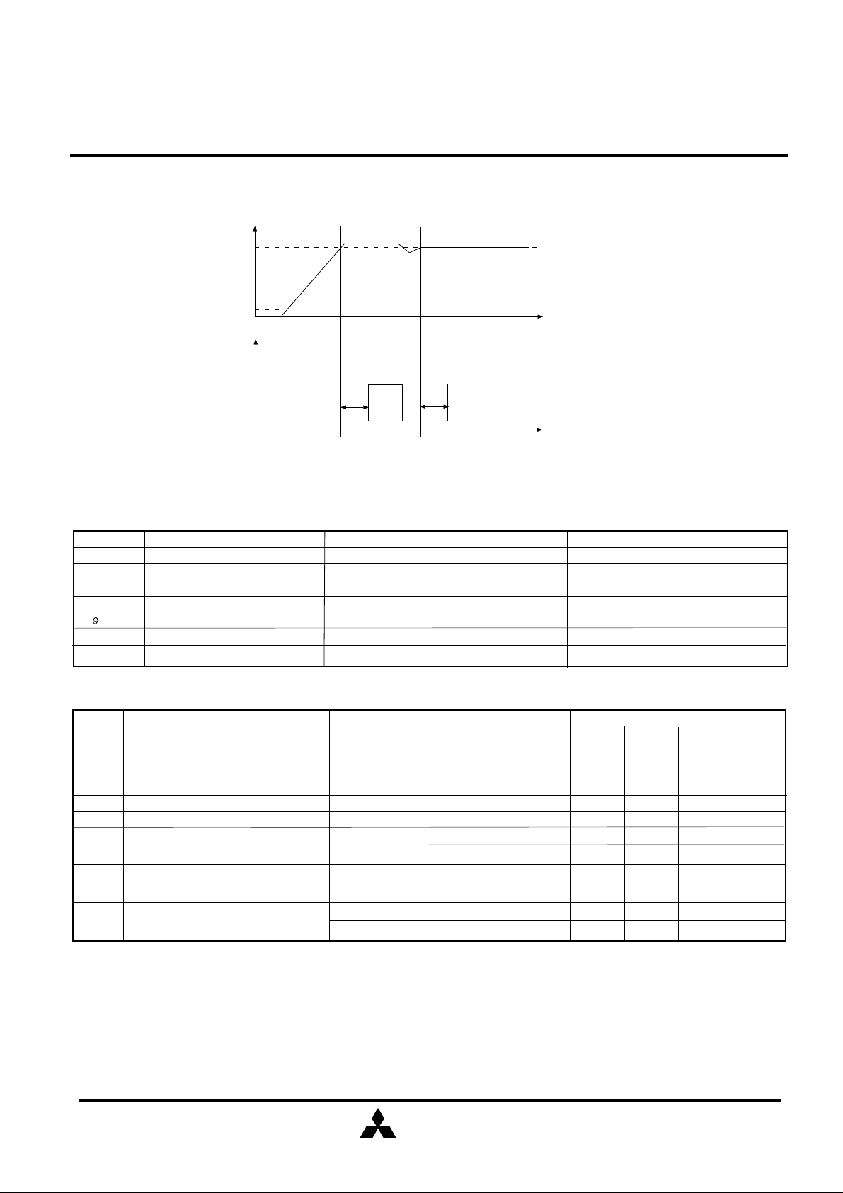
OPERATION WAVEFORM
4.45V
SUPPLY VOLTAGE
MITSUBISHI<Dig.Ana.INTERFACE>
M62022L,FP
VOLTAGE DETECTING,SYSTEM RESETTING IC
OUTPUT STATUS
0.65V
H
L
OUTPUT UNSETTLED
~
td 0.34XCd(pF)µsec
~
td
td
t
t
ABSOLUTE MAXIMUM RATINGS (Ta=25°C, unless otherwise noted)
Symbol Ratings
VCC
ISINK
Vo
Pd
K
Topr
Tstg
Supply voltage
Output sink current
Output voltage
Power dissipation
Thermal derating
Operating temperature
Storage temperature
Parameter
(Ta≥25°C)
Conditions
450(SIP)/300(FP)
4.5(SIP)/3.0(FP)
-30 ~ +85
-40 ~ +125
ELECTRICAL CHARACTERISTICS (Ta=25°C, unless otherwise noted)
Symbol
Vs
Detection voltage
∆Vs
Hysteresis voltage
Coefficient of detection voltage to temperature
Vs/∆T
Circuit current
ICC
Delay time
tpd
Ipd
Delay current
Vsat
Output saturation voltage
Limit operating voltage
VOPL
Output leak current
IOH
Note.Delay time can be varied by changing the capacitance.
Parameter
Vcc=5V
Ta=-30~+85°C Cd=0.01µF(Note)
Vcc=5V
RL=2.2kΩ Vsat≤0.4V
RL=100kΩ Vsat≤0.4V
Ta=-30~+85°C
Test conditions
Isink=4mA
Min.
4.30
30 80
1.6
-8
18
6
18
Limits
Typ.
4.45
50
0.01
420
3.4
-5
0.2
0.67
0.55
Max.
4.60
630
7.0
-3
0.4
0.80
0.70
30
1
Unit
V
mA
V
mW
mW/°C
°C
°C
Unit
V
mV
%/°C
µA
ms
µA
V
V
nA
µA
MITSUBISHI
ELECTRIC
2
( / 2 )
 Loading...