

Mitsubishi M5M5256DVP-70XL, M5M5256DRV-70XL, M5M5256DVP-55XL, M5M5256DVP-55LL, M5M5256DVP-45XL Datasheet
...
'97.4.7
MITSUBISHI LSIs
M5M5256DP,FP,VP,RV -45LL,-55LL,-70LL,
-45XL,-55XL,-70XL
262144-BIT (32768-WORD BY 8-BIT) CMOS STATIC RAM
DESCRIPTION
The M5M5256DP,FP,VP,RV is 262,144-bit CMOS static RAMs
organized as 32,768-words by 8-bits which is fabricated using
high-performance 3 polysilicon CMOS technology. The use of
resistive load NMOS cells and CMOS periphery results in a high
density and low power static RAM. Stand-by current is small
enough for battery back-up application. It is ideal for the memory
systems which require simple interface.
Especially the M5M5256DVP,RV are packaged in a 28-pin thin
small outline package.Two types of devices are available,
M5M5256DVP(normal lead bend type package),
M5M5256DRV(reverse lead bend type package). Using both types of
devices, it becomes very easy to design a printed circuit board.
FEATURE
Type
M5M5256DP, FP,VP,RV-45LL
M5M5256DP, FP,VP,RV-55LL
M5M5256DP, FP,VP,RV-70LL
M5M5256DP, FP,VP,RV-45XL 45ns
M5M5256DP, FP,VP,RV-55XL
M5M5256DP, FP,VP,RV-70XL
•Single +5V power supply
•No clocks, no refresh
•Data-Hold on +2.0V power supply
•Directly TTL compatible : all inputs and outputs
•Three-state outputs : OR-tie capability
•/OE prevents data contention in the I/O bus
•Common Data I/O
•Battery backup capability
•Low stand-by current··········0.05µA(typ.)
Access
time
Power supply current
(max)
45ns
55ns
70ns
55ns
70ns
Active
(max)
55mA
(Vcc=5.5V)
Stand-by
(max)
20µA
(Vcc=5.5V)
5µA
(Vcc=5.5V)
0.05µA
(Vcc=3.0V,
Typical)
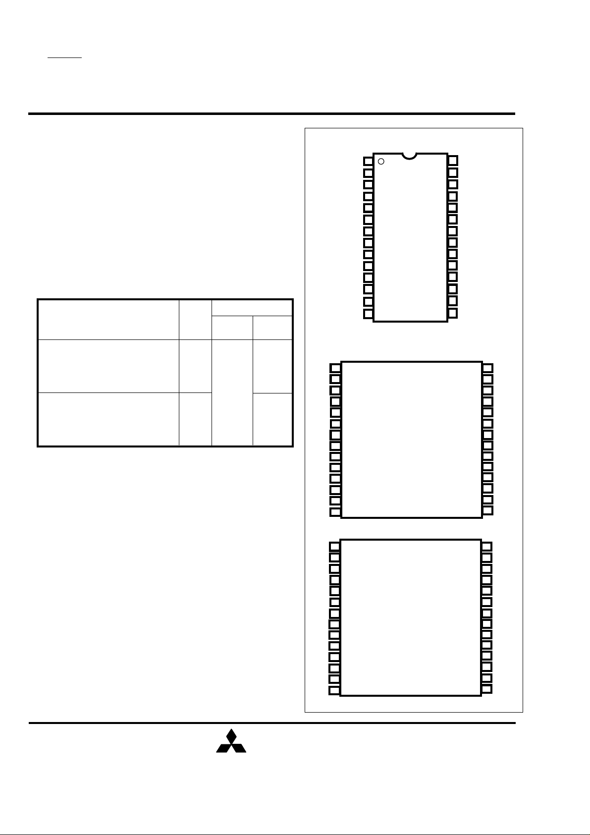
PACKAGE
M5M256DP : 28 pin 600 mil DIP
M5M5256DFP : 28 pin 450 mil SOP
M5M5256DVP,RV : 28pin 8 X 13.4 mm TSOP
2
APPLICATION
Small capacity memory units
PIN CONFIGURATION (TOP VIEW)
A14
A12
A5
A4
A3
A0
DQ1
DQ2
GND
22
23
27
1
2
3
4 A6
5 A5
6 A4
7 A3
7
6
5
4
3
2
1
28
27
26
25
24
23
22
1
2
3A7
4A6
5
6
7
8A2
9A1
10
11
12
13DQ3
14
Outline 28P4 (DP)
/OE
A11
A924
A825
A1326
/W
Vcc28
A14
A12
A7
A3
A4
A5
A6
A7
A12
A14
/W
A13
A8
A9
A11
/OE
M5M5256DVP
Outline 28P2C-A (DVP)
M5M5256DRV
Outline 28P2C-B (DRV)
M5M5256DP,FP
28P2W-C (DFP)
Vcc
28
/W
27
26
A13
A8
25
24 A9
A11
23
22 /OE
21
A10
20
/S
19
DQ8
18 DQ7
DQ6
17
DQ5
16
DQ4
15
A10
DQ8
DQ7 18
DQ6 17
DQ5 16
DQ415
GND
DQ2
DQ1
A0
A1
A2
A1
A0
DQ1
DQ2
DQ3
GND
DQ4Vcc
DQ5
DQ6
DQ7
DQ8
/S
A10
/S
21
20
19
14
13DQ3
12
11
10
9
8A2
8
9
10
11
12
13
14
15
16
17
18
19
20
21
MITSUBISHI
ELECTRIC
1
'97.4.7
M5M5256DP,FP,VP,RV -45LL,-55LL,-70LL,
-45XL,-55XL,-70XL
262144-BIT (32768-WORD BY 8-BIT) CMOS STATIC RAM
FUNCTION
The operation mode of the M5M5256DP,FP,VP,RV is
determined by a combination of the device control inputs /S,
/W and /OE. Each mode is summarized in the function table.
A write cycle is executed whenever the low level /W
overlaps with the low level /S. The address must be set up
before the write cycle and must be stable during the entire
cycle. The data is latched into a cell on the trailing edge of
/W, /S, whichever occurs first, requiring the set-up and hold
time relative to these edge to be maintained. The output
enable /OE directly controls the output stage. Setting the
/OE at a high level,the output stage is in a high-impedance
state, and the data bus contention problem in the write cycle
is eliminated.
FUNCTION TABLE
A read cycle is executed by setting /W at a high level and
/OE at a low level while /S are in an active state.
When setting /S at a high level, the chip is in a
non-selectable mode in which both reading and writing are
disabled. In this mode, the output stage is in a
high-impedance state, allowing OR-tie with other chips and
memory expansion by /S. The power supply current is
reduced as low as the stand-by current which is specified
as Icc3 or Icc4, and the memory data can be held at +2V
power supply, enabling battery back-up operation during
power failure or power-down operation in the non-selected
mode.
MITSUBISHI LSIs
/S /W /OE
H
L
L
L
BLOCK DIAGRAM
A 8
A 13
A 14
A 12
A 7
A 6
A 5
INPUT
INPUT
INPUT
A 4
A 3
A 2
A 1
A 0
A 10
A 11
A 9
/W
/S
/OE
ADDRESS
INPUT
WRITE CONTROL
CHIP SELECT
OUTPUT ENABLE
X X
L X
H
H
25
26
1
2
2
3
4
5
6
7
8
9
10
21
23
24
27
20
22
Non selection
L
H
BUFFER
ADDRESS INPUT
BUFFER
ADDRESS INPUT
Mode DQ Icc
Stand-by
Active
Active
Active
SENSE ANPLIFIER
Write
Read
ROW DECODER
COLUMN
DECODER
High-impedance
DIN
DOUT
High-impedance
32768 WORD
X 8BIT
(512 ROWS X
512 COLUMNS)
CLOCK
GENERATOR
OUTPUT BUFFER
BUFFER
DATA INPUT
11
DQ1
12
DQ2
13
DQ3
15
DQ4
DATA I/O
DQ5
16
DQ6
17
18
DQ7
DQ8
19
VCC
28
(5V)
GND
14
(0V)
MITSUBISHI
ELECTRIC
2
'97.4.7
MITSUBISHI LSIs
M5M5256DP,FP,VP,RV -45LL,-55LL,-70LL,
-45XL,-55XL,-70XL
262144-BIT (32768-WORD BY 8-BIT) CMOS STATIC RAM
ABSOLUTE MAXIMUM RATINGS
Symbol
Vcc
VI
VO
Pd
Topr
Tstg
* -3.0V in case of AC ( Pulse width ≤ 30ns )
Supply voltage
Input voltage
Output voltage
Power dissipation
Operating temperature
Storage temperature
DC ELECTRICAL CHARACTERISTICS (Ta=0~70°C, Vcc=5V±10%, unless otherwise noted)
Parameter
Conditions
With respect to GND
Ta=25°C 700
Ratings
-0.3*~7.0
-0.3*~Vcc+0.3
(Max 7.0)
0~Vcc
0~70
-65~150
Unit
V
V
V
mW
°C
°C
Symbol Parameter
VIH High-level input voltage
VIL Low-level input voltage
VOH1 High-level output voltage 1 IOH=-1mA
VOH2 High-level output voltage 2 IOH=-0.1mA
VOL Low-level output voltage IOL=2mA
II
IO Output current in off-state
Icc1
Icc2
Icc3 Stand-by current
Input current VI=0~Vcc
/S=VIH or or /OE=VIH,
VI/O=0~Vcc
Active supply current
(AC, MOS level )
Active supply current
(AC, TTL level )
/S≤0.2V,
Other inputs<0.2V or >Vcc-0.2V
Output-open Min. cycle
/S=VIL,
other inputs=VIH or VIL
Output-open Min. cycle
/S≥Vcc-0.2V,
other inputs=0~Vcc
Test conditions
45ns
70ns
45ns
70ns
-LL
-XL
2.2
-0.3
2.4
Vcc
-0.5
Limits
0.1
MaxTypMin
Vcc
+0.3
0.8
0.4
±1
±1
5035
453055ns
4025
5535
503055ns
4525
20
Unit
V
V
V
V
V
uA
uA
mA
mA
uA
5
Stand-by currentIcc4
* -3.0V in case of AC ( Pulse width ≤ 30ns )
/S=VIH,other inputs=0~Vcc
CAPACITANCE (Ta=0~70°C, Vcc=5V±10%, unless otherwise noted)
Symbol Parameter Test conditions
CI
CO
Note 0: Direction for current flowing into an IC is positive (no mark).
1: Typical value is one at Ta = 25°C.
2: CI, CO are periodically sampled and are not 100% tested.
Input capacitance
Output capacitance
VI=GND, VI=25mVrms, f=1MHz
VO=GND,VO=25mVrms, f=1MHz
MITSUBISHI
ELECTRIC
Limits
TypMin
Max
6
8
mA
3
Unit
pF
pF
3

'97.4.7
MITSUBISHI LSIs
M5M5256DP,FP,VP,RV -45LL,-55LL,-70LL,
-45XL,-55XL,-70XL
262144-BIT (32768-WORD BY 8-BIT) CMOS STATIC RAM
AC ELECTRICAL CHARACTERISTICS (Ta = 0~70°C, Vcc=5V±10%, unless otherwise noted )
(1) MEASUREMENT CONDITIONS
Input pulse level···················VIH=2.4V,VIL=0.6V
Input rise and fall time··········5ns
Reference level····················VOH=VOL=1.5V
Output loads·························Fig.1,CL=30pF (-45LL,-45XL )
CL=50pF (-55LL,-55XL )
CL=100pF (-70LL,-70XL )
CL=5pF (for ten,tdis)
Transition is measured ±500mV from steady
state voltage. (for ten,tdis)
(2) READ CYCLE
Symbol Parameter
tCR Read cycle time
ta(A)
ta(S)
ta(OE)
tdis(S)
tdis(OE)
ten(S)
ten(OE)
tV(A)
Address access time
Chip select access time
Output enable access time
Output disable time after /S high
Output disable time after /OE high
Output enable time after /S low
Output enable time after /OE low
Data valid time after address
-45LL, XL -55LL, XL
Min
Max
45
45
45
25
15
15
5
5
10
Limits
Min
55
5
5
10
DQ
(Including
scope and JIG)
-70LL, XL
Max
70
55
55
30
20
20
10
990Ω
Fig.1 Output load
MaxMin
70
70
35
25
25
5
5
Vcc
1.8kΩ
CL
Unit
ns
ns
ns
ns
ns
ns
ns
ns
ns
(3) WRITE CYCLE
Symbol Parameter
tCW
tw(W)
tsu(A)
tsu(A-WH)
tsu(S)
tsu(D)
th(D)
trec(W)
tdis(W)
tdis(OE)
ten(W)
ten(OE)
Write cycle time
Write pulse width
Address setup time
Address setup time with respect to /W high
Chip select setup time
Data setup time
Data hold time
Write recovery time
Output disable time from /W low
Output disable time from /OE high
Output enable time from /W high
Output enable time from /OE low
Min
MITSUBISHI
ELECTRIC
45
35
40
40
20
Limits
-70LL, XL-45LL, XL -55LL, XL
Max
Min
Max
55
40
0
0
0
15
15
5
5
0
50
50
25
0
0
20
20
5
5
MaxMin
70
50
0
65
65
30
0
0
5
5
25
25
Unit
ns
ns
ns
ns
ns
ns
ns
ns
ns
ns
ns
ns
4

'97.4.7
-45XL,-55XL,-70XL
(4) TIMING DIAGRAMS
Read cycle
A0~14
/S
/OE
MITSUBISHI LSIs
M5M5256DP,FP,VP,RV -45LL,-55LL,-70LL,
262144-BIT (32768-WORD BY 8-BIT) CMOS STATIC RAM
tCR
(Note 3)
(Note 3)
ta(A)
ta (S)
ta (OE)
ten (OE)
ten (S)
tv (A)
tdis (S)
tdis (OE)
(Note 3)
(Note 3)
DQ1~8
/W = "H" level
Write cycle (/W control mode)
A0~14
/S
(Note 3)
/OE
/W
DQ1~8
(Note 3) (Note 3)
tdis (OE)
tCW
tsu (S)
tsu (A-WH)
tw (W) trec (W)tsu (A)
tdis (W)
DATA VALID
(Note 3)
ten(OE)
ten (W)
DATA IN
STABLE
th (D)tsu (D)
MITSUBISHI
ELECTRIC
5

'97.4.7
-45XL,-55XL,-70XL
Write cycle ( /S control mode)
A0~14
MITSUBISHI LSIs
M5M5256DP,FP,VP,RV -45LL,-55LL,-70LL,
262144-BIT (32768-WORD BY 8-BIT) CMOS STATIC RAM
tCW
/S
/W
DQ1~8
tsu (A)
(Note 5)
(Note 3)
Note 3 : Hatching indicates the state is "don't care".
4 : Writing is executed in overlap of /S and /W low.
5 : If /W goes low simultaneously with or prior to /S, the outputs remain in the high impedance state.
6 : Don't apply inverted phase signal externally when DQ pin is output mode.
7 : ten, tdis are periodically sampled and are not 100% tested.
tsu (S) trec (W)
(Note 4)
tsu (D)
DATA IN
STABLE
th (D)
(Note 3)
MITSUBISHI
ELECTRIC
6

'97.4.7
MITSUBISHI LSIs
M5M5256DP,FP,VP,RV -45LL,-55LL,-70LL,
-45XL,-55XL,-70XL
262144-BIT (32768-WORD BY 8-BIT) CMOS STATIC RAM
POWER DOWN CHARACTERISTICS
(1) ELECTRICAL CHARACTERISTICS (Ta = 0~70°C, Vcc=5V±10%, unless otherwise noted)
Symbol Parameter
Vcc (PD)
VI (/S) Chip select input /S
Icc (PD)
Note7: ICC (PD) = 1uA in case of Ta = 25°C
Note8: ICC (PD) = 0.2uA in case of Ta = 25°C
Power down supply voltage
Power down supply current
Test conditions Unit
2.2V≤VCC(PD)
2V≤VCC(PD)≤2.2V
Vcc = 3V,/S≥Vcc-0.2V,
Other inputs=0~Vcc
-LL
-XL
Limits
Min
2
2.2
VCC(PD)
0.05
MaxTyp
10
(Note 7)
2
(Note 8)
V
V
V
uA
(2) TIMING REQUIREMENTS (Ta = 0~70°C, Vcc=5V±10%, unless otherwise noted )
Symbol
tsu (PD)
trec (PD)
Power down set up time
Power down recovery time
Parameter
Test conditions
Min
(3) POWER DOWN CHARACTERISTICS
/S control mode
Vcc
/S
2.2V
tsu (PD)
4.5V
/S≥Vcc-0.2V
4.5V
trec (PD)
Limits
MaxTyp
0
Unit
ns
tCR ns
2.2V
MITSUBISHI
ELECTRIC
7
 Loading...