

查询M5M465165DJ供应商
EDO MODE 67108864-BIT (16777216-WORD BY 4-BIT) DYNAMIC RAM
EDO MODE 67108864-BIT (8388608-WORD BY 8-BIT) DYNAMIC RAM
EDO MODE 67108864-BIT (4194304-WORD BY 16-BIT) DYNAMIC RAM
MITSUBISHI LSIs(Rev. 1.0)
M5M467405/465405DJ,DTP -5,-6,-5S,-6S
M5M467805/465805DJ,DTP -5,-6,-5S,-6S
M5M465165DJ,DTP -5,-6,-5S,-6S
PRELIMINARY
Some of contents are subject to change without notice.
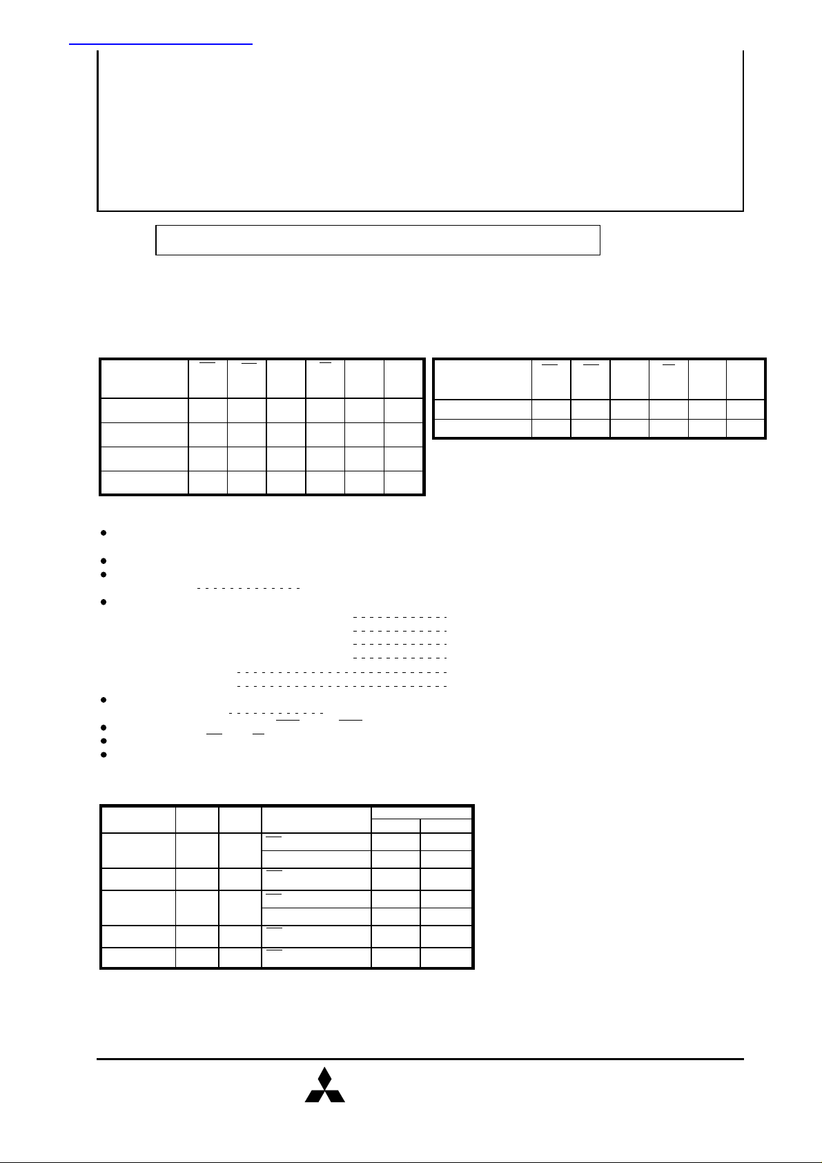
DESCRIPTION
The M5M467405/465405DJ,DTP is a 16777216-word by 4-bit, M5M467805/465805DJ,DTP is a 8388608-word by 8-bit, and
M5M465165DJ,DTP is a 4194304-word by 16-bit dynamic RAMs, fabricated with the high performance CMOS process, and are
suitable for large-capacity memory systems with high speed and low power dissipation.
FEATURES
CAS
access
time
(max.ns)
13
15
13
Address
access
time
(max.ns)
OE
access
time
(min.ns)
(max.ns)
25
13
30
15
25
13
(M5M467405Dxx/M5M465405Dxx/M5M467805Dxx/M5M465805Dxx)
(M5M465165Dxx)
RAS
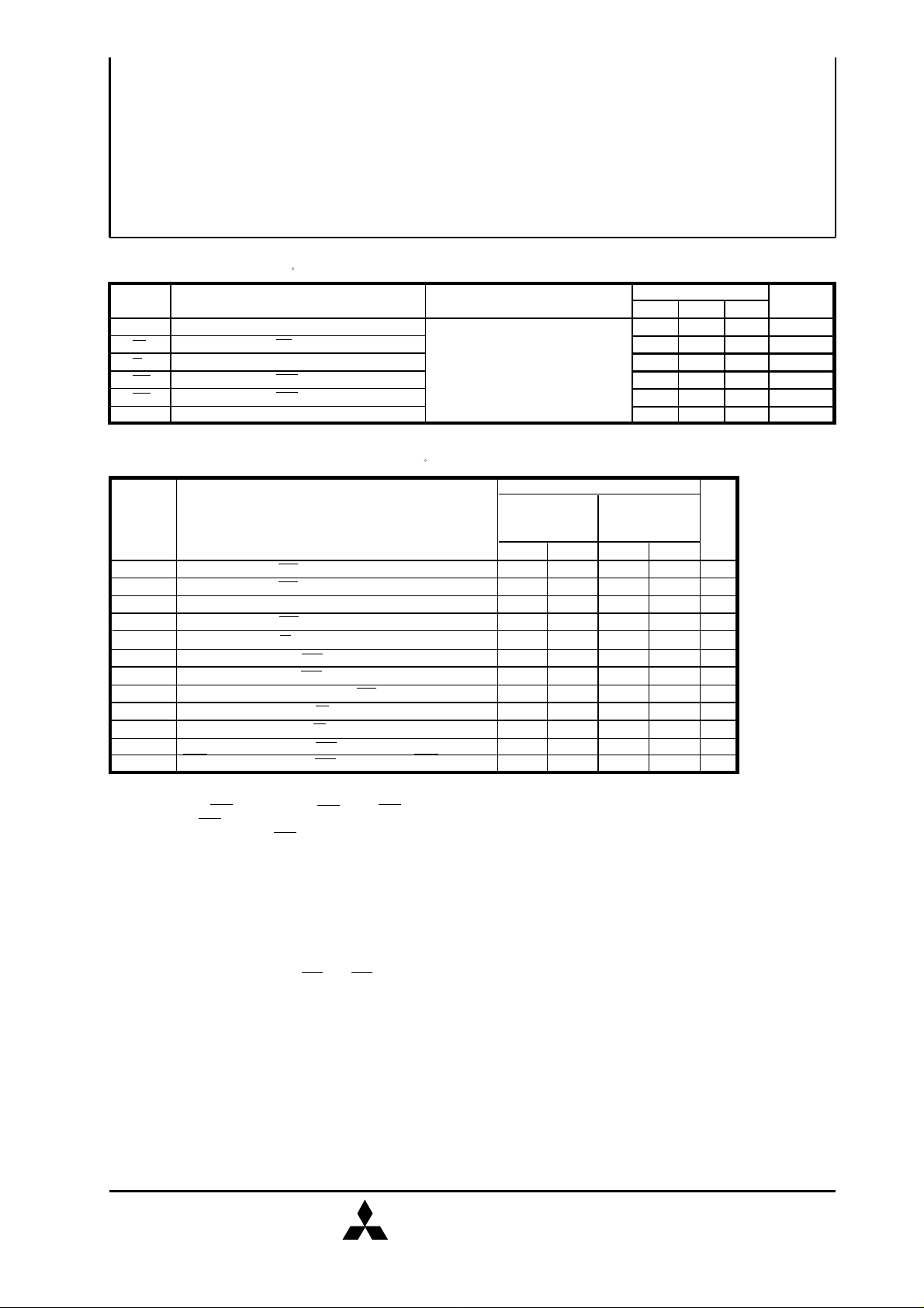
Type name
M5M467405DXX-5,5S
M5M467805DXX-5,5S
M5M467405DXX-6,6S
M5M467805DXX-6,6S
M5M465405DXX-5,5S
M5M465805DXX-5,5S
M5M465405DXX-6,6S
M5M465805DXX-6,6S
XX=J,TP
access
time
(max.ns)
50
60
50
60 15 30 104 32515
Standard 32 pin SOJ, 32 pin TSOP
Standard 50 pin SOJ, 50 pin TSOP
Single 3.3 0.3V supply
±
Low stand-by power dissipation
1.8mW (Max) LVCMOS input level
Low operating power dissipation
M5M467405Dxx-5,5S / M5M467805Dxx-5,5S 360.0mW (Max)
M5M467405Dxx-6,6S / M5M467805Dxx-6,6S 324.0mW (Max)
M5M465405Dxx-5,5S / M5M465805Dxx-5,5S 468.0mW (Max)
M5M465405Dxx-6,6S / M5M465805Dxx-6,6S 432.0mW (Max)
M5M465165Dxx-5,5S 504.0mW (Max)
M5M465165Dxx-6,6S 468.0mW (Max)
Self refresh capability*
Self refresh current 400µA (Max)
EDO mode , Read-modify-write, CAS before RAS refresh, Hidden refresh capabilities
Early-write mode , OE and W to control output buffer impedance
All inputs, outputs LVTTL compatible and low capacitance
:Applicable to self refresh version(M5M467405/465405/467805/465805/465165DJ,DTP-5S,-6S:option) only
*
Cycle
time
84
104
84
Power
dissipa-
tion
(typ.mW)
300
250
390
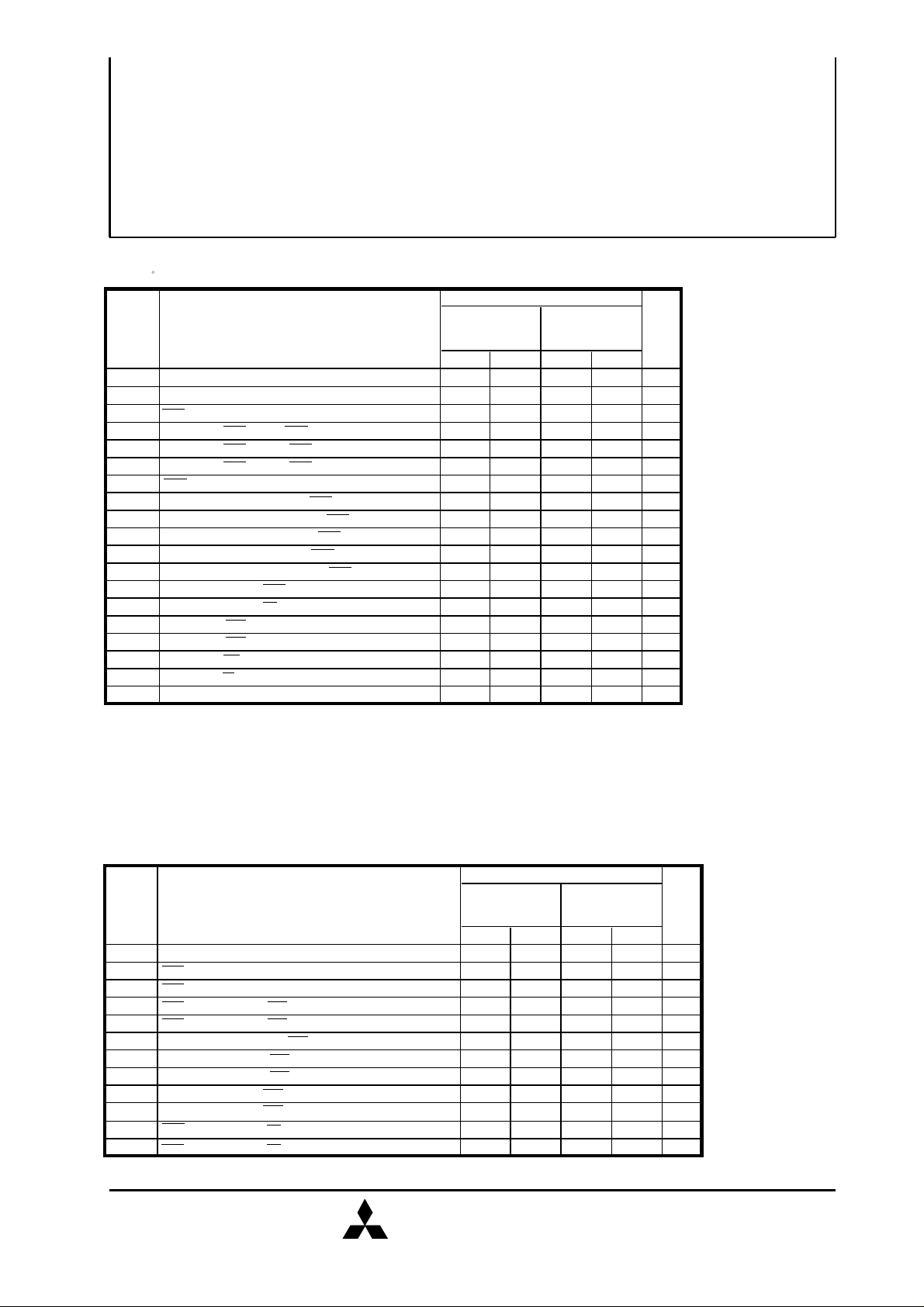
Type name
M5M465165DXX-5,5S
M5M465165DXX-6,6S
RAS
access
time
(max.ns)
50
60
CAS
access
time
(max.ns)
13
15
Address
access
time
(max.ns)
25
30
OE
access
time
(max.ns)
13
15
Cycle
time
(min.ns)
84
104
Power
dissipa-
tion
(typ.mW)
420
390
ADDRESS
Part No.
M5M467405Dxx
M5M465405Dxx
M5M467805Dxx
M5M465805Dxx
M5M465165Dxx
Row Add. Col. Add.
A0-A12
A0-A11 A0-A11
A0-A12
A0-A11
A0-A11
A0-A10
A0-A9
A0-A10
A0-A9
Refresh
RAS Only Ref,Normal R/W
CBR Ref,Hidden Ref
RAS Only Ref,Normal R/W
CBR Ref,Hidden Ref
RAS Only Ref,Normal R/W
CBR Ref,Hidden Ref
RAS Only Ref,Normal R/W
CBR Ref,Hidden Ref
RAS Only Ref,Normal R/W
CBR Ref,Hidden Ref
Refresh Cycle
Normal S-version
8192/64ms
4096/64ms
4096/64ms
8192/64ms
4096/64ms
4096/64ms
4096/64ms
8192/128ms
4096/128ms
4096/128ms
8192/128ms
4096/128ms
4096/128ms
4096/128ms
APPLICATION
Main memory unit for computers, Microcomputer memory, Refresh memory for CRT
1
MITSUBISHI ELECTRIC
Aug. 1999
M5M467405/465405DJ,DTP -5,-6,-5S,-6S
M5M467805/465805DJ,DTP -5,-6,-5S,-6S
M5M465165DJ,DTP -5,-6,-5S,-6S
EDO MODE 67108864-BIT (16777216-WORD BY 4-BIT) DYNAMIC RAM
EDO MODE 67108864-BIT (8388608-WORD BY 8-BIT) DYNAMIC RAM
EDO MODE 67108864-BIT (4194304-WORD BY 16-BIT) DYNAMIC RAM
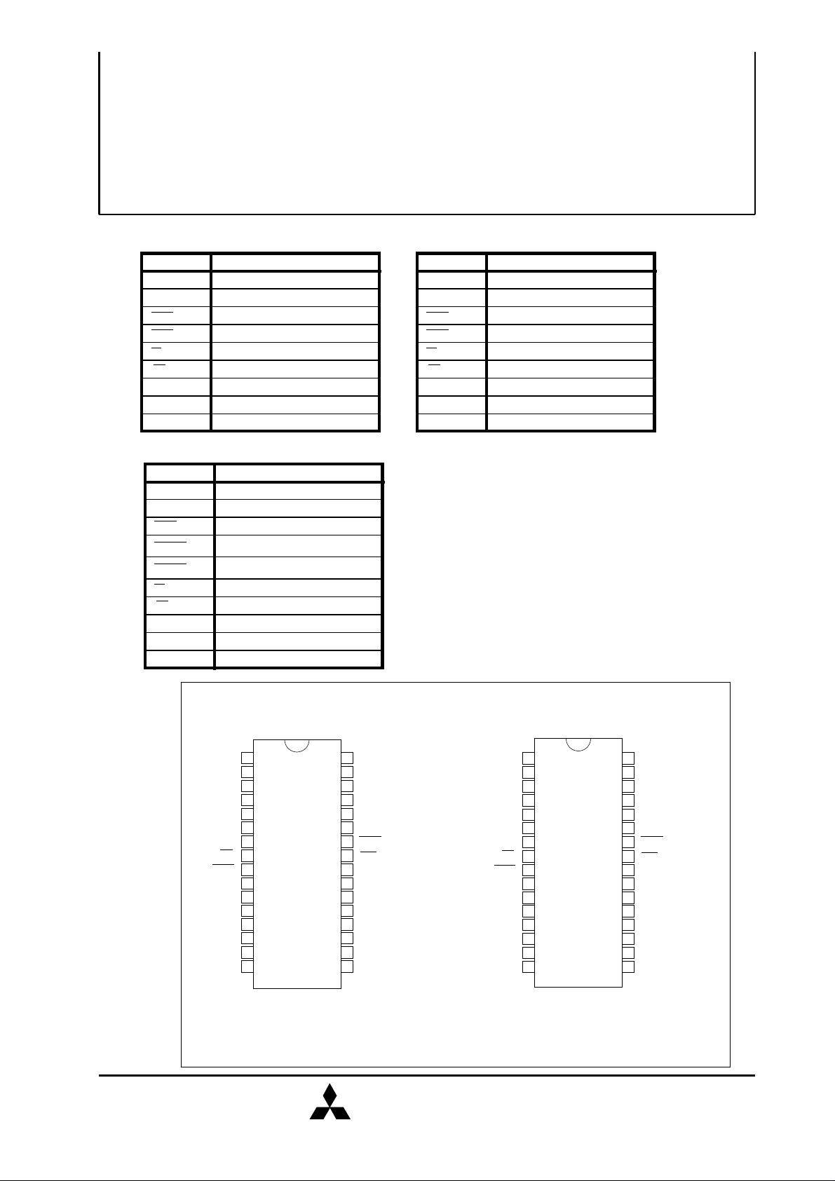
PIN DESCRIPTION
M5M467405Dxx / M5M465405Dxx
Pin Name
A0-A12
DQ1-DQ4
RAS
CAS
W
OE
Vcc
Vss
NC No Connection
M5M465165Dxx
Pin Name
A0-A11
DQ1-DQ16
RAS
UCAS
LCAS
W
OE
Vcc
Vss
NC No Connection
Function
Address Inputs
Data Inputs / Outputs
Row Address Strobe Input
Column Address Strobe Input
Write Control Input
Output Enable Input
Power Supply (+3.3V)
Ground (0V)
Function
Address Inputs
Data Inputs / Outputs
Row Address Strobe Input
Upper byte control
Column Address Strobe Input
Lower byte control
Column Address Strobe Input
Write Control Input
Output Enable Input
Power Supply (+3.3V)
Ground (0V)
M5M467805Dxx / M5M465805Dxx
Pin Name
A0-A12
DQ1-DQ8
RAS
CAS
W
OE
Vcc
Vss
Function
Address Inputs
Data Inputs / Outputs
Row Address Strobe Input
Column Address Strobe Input
Write Control Input
Output Enable Input
Power Supply (+3.3V)
Ground (0V)
NC No Connection
XX=J, TP
MITSUBISHI LSIs(Rev. 1.0)
M5M467400/465400DJ, DTP
1
Vcc
2
DQ1
DQ2
3
NC
4
M5M465405DJ
NC
NC
NC
W
RAS
A0
A1
A2
A3
A4
A5
Vcc
5
6
7
8
9
10
11
12
13
14
15
16
M5M467405DJ
Outline 32P0N (400mil SOJ)
2
PIN CONFIGURATION (TOP VIEW)
32
Vss
31
DQ4
30
DQ3
29
NC
28
NC
NC
27
26
CAS
25
OE
24
A12/NC(Note)
23
A11
22
A10
A9
21
20
A8
19
A7
18
A6
17
Vss
Vcc
DQ1
DQ2
NC
NC
NC
NC
W
RAS
A0
A1
A2
A3
A4
A5
Vcc
Outline 32P3N (400mil TSOP Normal Bend)
:
Note
:
NC
1
2
3
4
M5M465405DTP
5
6
7
8
9
10
11
12
13
14
15
16
A12...M5M467405Dxx, NC...M5M465405Dxx
NO CONNECTION
32
Vss
31
DQ4
30
DQ3
29
M5M467405DTP
NC
28
NC
NC
27
26
CAS
25
OE
24
A12/NC(Note)
23
A11
22
A10
A9
21
20
A8
19
A7
18
A6
17
Vss
Aug. 1999
MITSUBISHI ELECTRIC
MITSUBISHI LSIs(Rev. 1.0)
M5M467405/465405DJ,DTP -5,-6,-5S,-6S
M5M467805/465805DJ,DTP -5,-6,-5S,-6S
M5M465165DJ,DTP -5,-6,-5S,-6S
EDO MODE 67108864-BIT (16777216-WORD BY 4-BIT) DYNAMIC RAM
EDO MODE 67108864-BIT (8388608-WORD BY 8-BIT) DYNAMIC RAM
EDO MODE 67108864-BIT (4194304-WORD BY 16-BIT) DYNAMIC RAM
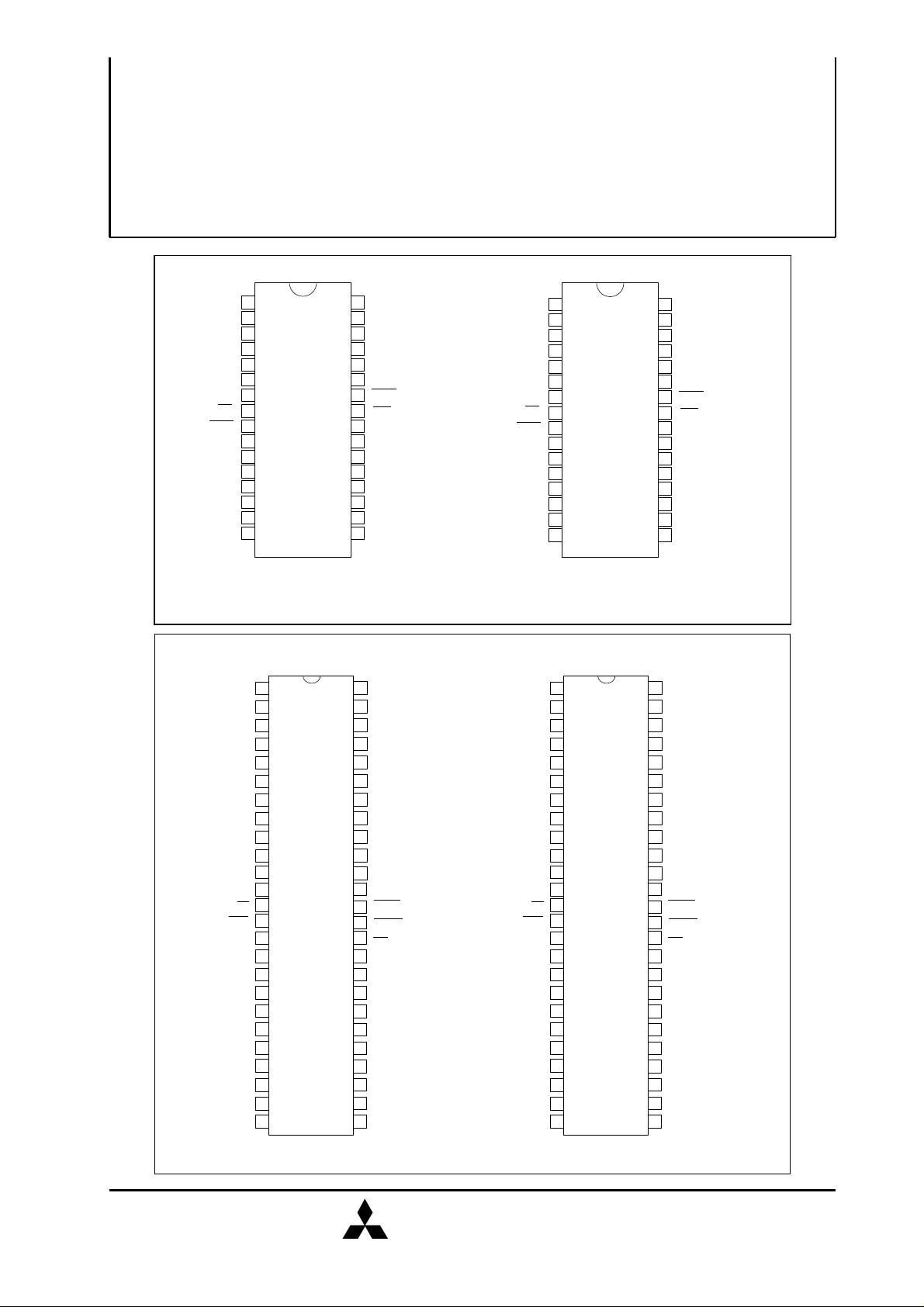
PIN CONFIGURATION (TOP VIEW)M5M467805/465805DJ, DTP
1
Vcc
2
DQ1
DQ2
3
4
DQ3
5
DQ4
6
NC
Vcc
7
8
W
9
RAS
10
A0
11
A1
A2
12
13
A3
14
A4
A5
15
16
Vcc
Outline 32P0N (400mil SOJ)
M5M465165DJ, DTP
1
Vcc Vss
DQ1
2
DQ2
3
4
DQ3
DQ4
5
Vcc
6
DQ5
7
8
DQ6
9
DQ7
10
DQ8
11
NC
12
12Vcc
13
W
14
RAS
NC
15
16
NC
17
NC
18
NC
19
A0
20
A1
21
A2
22
A3
23
A4
A5
24
25
Vcc
Outline 50P0G (400mil SOJ)
32
31
30
M5M465805DJ
29
M5M467805DJ
28
27
26
25
24
23
22
21
20
19
18
17
Note A12...M5M467800Dxx, NC...M5M465800Dxx
NC
PIN CONFIGURATION (TOP VIEW)
50
49
48
47
46
45
44
43
42
M5M465165DJ
41
40
39
38
37
36
35
34
33
32
31
30
29
28
27
26
Vss
DQ8
DQ7
DQ6
DQ5
Vss
CAS
OE
A12/NC(Note)
A11
A10
A9
A8
A7
A6
Vss
:
:
NO CONNECTION
DQ16
DQ15
DQ14
DQ13
Vss
DQ12
DQ11
DQ10
DQ9
NC
Vss
LCAS
UCAS
OE
NC
NC
NC
A11
A10
A9
A8
A7
A6
Vss
NC : NO CONNECTION
Vcc
DQ1
DQ2
DQ3
DQ4
NC
Vcc
W
RAS
A0
A1
A2
A3
A4
A5
Vcc
1
2
3
4
M5M465805DTP
5
6
7
8
9
10
11
12
13
14
15
16
32
Vss
31
DQ8
30
DQ7
DQ6
29
M5M467805DTP
DQ5
28
27
Vss
26
CAS
25
OE
24
A12/NC(Note)
23
A11
22
A10
A9
21
20
A8
19
A7
18
A6
17
Vss
Outline 32P3N (400mil TSOP Normal Bend)
Vcc
DQ1
DQ2
DQ3
DQ4
Vcc
DQ5
DQ6
DQ7
DQ8
NC
RAS
NC
NC
NC
NC
A0
A1
A2
A3
A4
A5
Vcc
1
2
3
4
5
6
7
8
9
10
W
15
16
17
18
19
22
25
M5M465165DTP
11
12
12Vcc
13
14
20
21
23
24
50
Vss
49
DQ16
48
DQ15
47
DQ14
46
DQ13
45
Vss
44
DQ12
43
DQ11
42
DQ10
41
DQ9
40
NC
Vss
39
LCAS
38
37
UCAS
36
OE
35
NC
34
NC
33
NC
32
A11
31
A10
30
A9
29
A8
28
A7
27
A6
26
Vss
Outline 50P3G (400mil TSOP Normal Bend)
3
Aug. 1999
MITSUBISHI ELECTRIC
MITSUBISHI LSIs(Rev. 1.0)
M5M467405/465405DJ,DTP -5,-6,-5S,-6S
M5M467805/465805DJ,DTP -5,-6,-5S,-6S
M5M465165DJ,DTP -5,-6,-5S,-6S
EDO MODE 67108864-BIT (16777216-WORD BY 4-BIT) DYNAMIC RAM
EDO MODE 67108864-BIT (8388608-WORD BY 8-BIT) DYNAMIC RAM
EDO MODE 67108864-BIT (4194304-WORD BY 16-BIT) DYNAMIC RAM
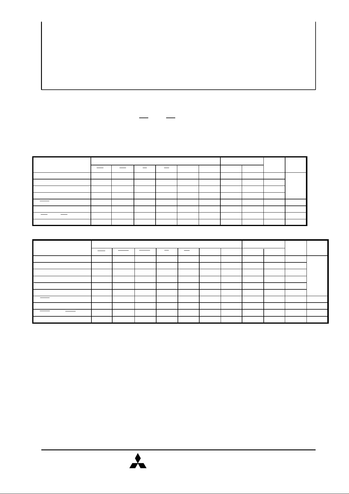
FUNCTION
The M5M467405(805)/465405(805,165)DJ, DTP provide, in addition to normal read, write, and read-modify-write operations,
a number of other functions, e.g., EDO mode, CAS before RAS refresh, and delayed-write.
The input conditions for each are shown in Table 1.
Table 1 Input conditions for each mode
M5M467405Dxx / M5M465405Dxx / M5M467805Dxx / M5M465805Dxx
Operation
Read
Write (Early write)
Write (Delayed write)
Read-modify-write
RAS-only refresh
Hidden refresh
CAS before RAS refresh
Standby
Inputs Input/Output
RAS CAS OE
ACT
ACT
ACT
ACT
ACT NAC DNC DNC APD DNC OPN OPN YES
ACT
ACT
NAC
ACT
ACT
ACT
ACT
ACT
ACT
DNC
W
NAC
ACT
ACT
ACT
NAC
NAC
DNC
ACT
DNC
DNC
ACT
ACT
DNC
DNC
Row
address address
APD
APD
APD
APD
DNC
DNC
DNC
Column
APD
APD
APD
APD
DNC
DNC
DNC
Input Output
OPN VLD
VLD
VLD
VLD
OPN
DNC
DNC
OPN
IVD
VLD
VLD
OPN
OPN
Refresh
NO
NO
NO
NO
YES
YES
NO
Remark
EDO mode
identical
M5M465165Dxx
Operation
Lower byte read
Upper byte read
Word read ACT ACT ACT NAC ACT
Lower byte write
Upper byte write
Word write
RAS-only refresh
Hidden refresh
CAS before RAS refresh
Stand-by
Note : ACT : active, NAC : nonactive, DNC : don' t care, VLD : valid, IVD : Invalid, APD : applied, OPN : open
RAS
ACT
ACT
ACT
ACT
ACT ACT ACT
ACT
ACT
ACT ACT ACT DNC DNC
NAC
LCAS
ACT
NAC NAC ACT
ACT
NAC
NAC NAC DNC
ACT
DNC
Inputs
UCAS
NAC
ACT
NAC
ACT
ACT
DNC
W
NAC
DNC
NAC ACT
DNC
OE
ACT
NACACT
NACACT
NACACT
DNC
Row
address address
APD
APD
APD
APD
APD
APD
APD
DNC
DNC
DNC
Column
APD
APD
APD
APD
APD
APD
DNC
DNC
DNC
DNC
Input/Output
DQ1~DQ8
VLD
OPN
DIN DNC
DIN DIN
OPN
OPN OPN
OPN OPN
DQ9~DQ16
OPN
VLD
VLDVLD
DINDNC
OPN
VLDVLD
Refresh
NO
NO
NO
NO
NO
NO
YES
YES
YES
NO
Remark
EDO mode
identical
4
Aug. 1999
MITSUBISHI ELECTRIC
M5M467405/465405DJ,DTP -5,-6,-5S,-6S
M5M467805/465805DJ,DTP -5,-6,-5S,-6S
M5M465165DJ,DTP -5,-6,-5S,-6S
EDO MODE 67108864-BIT (16777216-WORD BY 4-BIT) DYNAMIC RAM
EDO MODE 67108864-BIT (8388608-WORD BY 8-BIT) DYNAMIC RAM
EDO MODE 67108864-BIT (4194304-WORD BY 16-BIT) DYNAMIC RAM
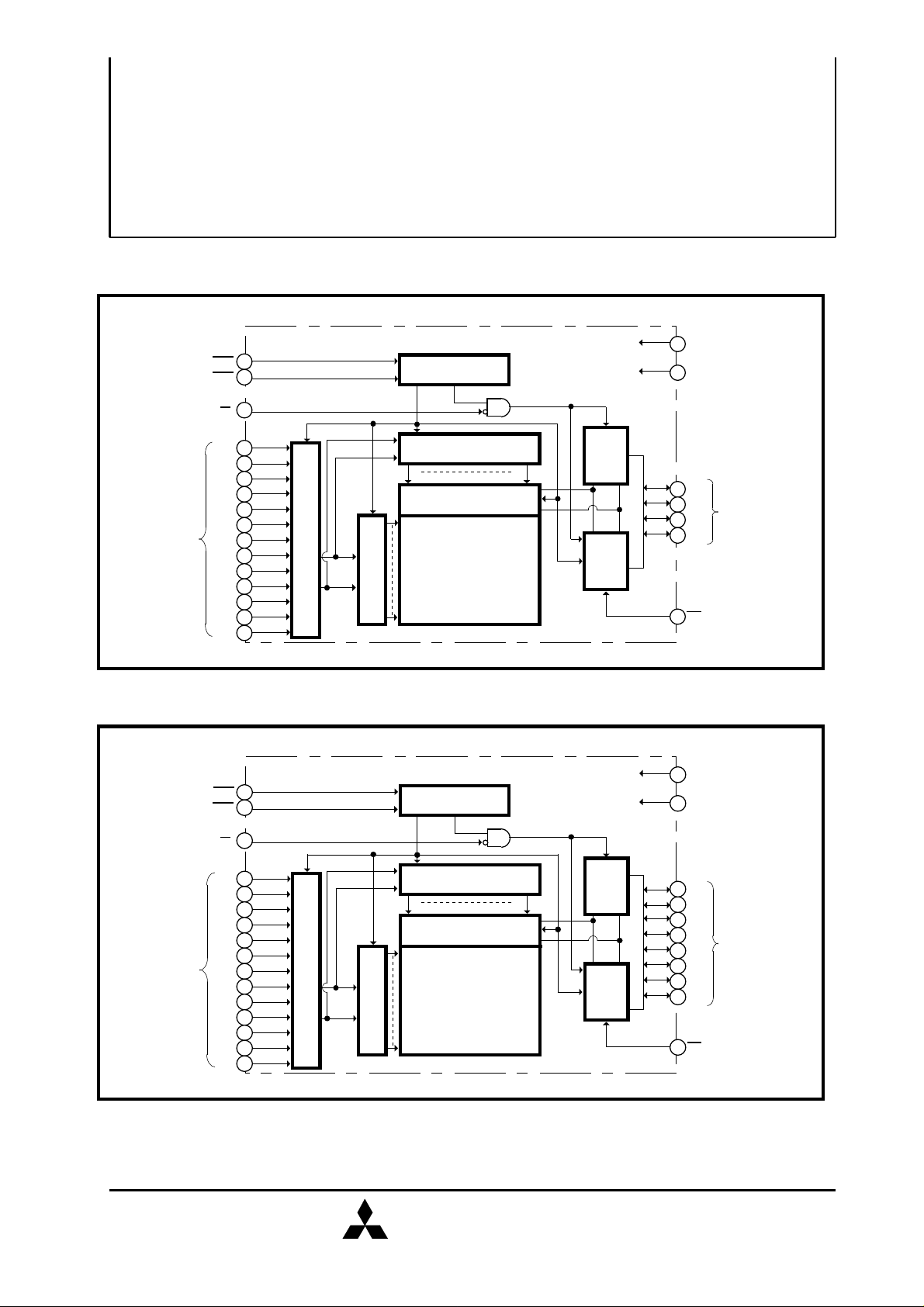
M5M467405Dxx / M5M465405Dxx
BLOCK DIAGRAM
MITSUBISHI LSIs(Rev. 1.0)
COLUMN ADDRESS
STROBE INPUT
ROW ADDRESS
STROBE INPUT
WRITE CONTROL
INPUT
ADDRESS INPUTS
CAS
RAS
W
A0
A1
A2
A3
A4
A5
A6
A7
A8
A9
A10
A11
A12
(Note)
ROW & COLUMN
Note Refer to Page 1 (ADDRESS)
M5M467805Dxx / M5M465805Dxx
BLOCK DIAGRAM
COLUMN ADDRESS
STROBE INPUT
ROW ADDRESS
STROBE INPUT
WRITE CONTROL
INPUT
ADDRESS INPUTS
CAS
RAS
W
A0
A1
A2
A3
A4
A5
A6
A7
A8
A9
A10
A11
A12
(Note)
ROW & COLUMN
Note Refer to Page 1 (ADDRESS)
A0~A11
(Note)
A0~
A12
ADDRESS BUFFER
(Note)
ROW DECODER
:
A0~A10
(Note)
A0~
A12
ADDRESS BUFFER
(Note)
ROW DECODER
:
CLOCK GENERATOR
CIRCUIT
COLUMN DECODER
SENSE REFRESH
AMPLIFIER & I /O CONTROL
MEMORY CELL
(67108864 BITS)
CLOCK GENERATOR
CIRCUIT
COLUMN DECODER
SENSE REFRESH
AMPLIFIER & I /O CONTROL
MEMORY CELL
(67108864 BITS)
(4)
DATA IN
(4)
DATA OUT
(8)
DATA IN
(8)
DATA OUT
BUFFERS
BUFFERS
BUFFERS
BUFFERS
Vcc (3.3V)
Vss (0V)
DQ1
DQ2
DATA
INPUTS / OUTPUTS
DQ3
DQ4
OUTPUT ENABLE
OE
INPUT
Vcc (3.3V)
Vss (0V)
DQ1
DQ2
DQ3
DQ4
DATA
INPUTS / OUTPUTS
DQ5
DQ6
DQ7
DQ8
OUTPUT ENABLE
OE
INPUT
5
Aug. 1999
MITSUBISHI ELECTRIC
M5M465165Dxx
BLOCK DIAGRAM
ROW ADDRESS
STROBE INPUT
LOWER BYTE CONTROL
COLUMN ADDRESS
STROBE INPUT
UPPER BYTE CONTROL
COLUMN ADDRESS
STROBE INPUT
WRITE CONTROL INPUT
ADDRESS INPUTS
MITSUBISHI LSIs(Rev. 1.0)
M5M467405/465405DJ,DTP -5,-6,-5S,-6S
M5M467805/465805DJ,DTP -5,-6,-5S,-6S
M5M465165DJ,DTP -5,-6,-5S,-6S
EDO MODE 67108864-BIT (16777216-WORD BY 4-BIT) DYNAMIC RAM
EDO MODE 67108864-BIT (8388608-WORD BY 8-BIT) DYNAMIC RAM
EDO MODE 67108864-BIT (4194304-WORD BY 16-BIT) DYNAMIC RAM
RAS
LCAS
UCAS
A0
A1
A2
A3
A4
A5
A6
A7
A8
A9
A10
A11
CLOCK GENERATOR
CIRCUIT
LOWER
DATA IN
BUFFERS
UPPER
W
A0~A9
ROW & COLUMN
A0 ~
ADDRESS BUFFER
A11
COLUMN DECODER
SENSE REFRESH
AMPLIFIER & I /O
CONTROL
MEMORY CELL
(67108864BITS)
ROW DECODER
(8)LOWER
BUFFERS
(8)LOWER
DATA OUT
DATA IN
(8)UPPER
BUFFERS
(8)UPPER
BUFFERS
DATA OUT
VCC (3.3V)
VSS (0V)
DQ1
DQ2
DQ8
DQ9
DQ10
DQ16
OE
LOWER DATA
INPUTS / OUTPUTS
UPPER DATA
INPUTS / OUTPUTS
OUTPUT ENABLE
INPUT
6
Aug. 1999
MITSUBISHI ELECTRIC
M5M467405/465405DJ,DTP -5,-6,-5S,-6S
M5M467805/465805DJ,DTP -5,-6,-5S,-6S
M5M465165DJ,DTP -5,-6,-5S,-6S
EDO MODE 67108864-BIT (16777216-WORD BY 4-BIT) DYNAMIC RAM
EDO MODE 67108864-BIT (8388608-WORD BY 8-BIT) DYNAMIC RAM
EDO MODE 67108864-BIT (4194304-WORD BY 16-BIT) DYNAMIC RAM
ABSOLUTE MAXIMUM RATINGS
Symbol
Vcc
VI
V0
I0
Pd
Topr
Tstg
Supply voltage
Input voltage
Output voltage
Output current
Power dissipation
Operating temperature
Storage temperature
Parameter Conditions Ratings Unit
With respect to Vss
Ta=25
C
MITSUBISHI LSIs(Rev. 1.0)
~
-0.5 4.6
~
-0.5 4.6
~
-0.5 4.6
50
1000
~
0 70
~
-65 150
V
V
V
mA
mW
C
C
RECOMMENDED OPERATING CONDITIONS
Symbol
Vcc
Vss
VIH
VIL
Note 1 : All voltage values are with respect to Vss.
Supply voltage
Supply voltage
High-level input voltage, all inputs
Low-level input voltage, all inputs
ELECTRICAL CHARACTERISTICS
Parameter
~
(Ta=0 70 , Vcc=3.3 0.3V, Vss=0V, unless otherwise noted) (Note 2)
[M5M467405D / M5M467805D]
Symbol
VOH
VOL
IOZ
I I
ICC1 (AV)
ICC2 (AV)
ICC4 (AV)
ICC6 (AV)
High-level output voltage
Low-level output voltage
Off-state output current
Input current
Average supply current
from Vcc
operating
Average supply current
from Vcc
stand-by
Average supply current
from Vcc
EDO-Mode
Average supply current
from Vcc
CAS before RAS refresh
mode
Parameter
(Note 3,4,5)
(Note 6)
(Note 3,4,5)
(Note 3,5)
M5M467405D-5,5S
M5M467805D-5,5S
M5M467405D-6,6S
M5M467805D-6,6S
M5M467405D-5,5S
-6,6S
M5M467805D-5,5S
-6,6S
M5M467405D-5,6
M5M467805D-5,6
M5M467405D-5S,6S
M5M467805D-5S,6S
M5M467405D-5,5S
M5M467805D-5,5S
M5M467405D-6,6S
M5M467805D-6,6S
M5M467405D-5,5S
M5M467805D-5,5S
M5M467405D-6,6S
M5M467805D-6,6S
(Ta=0 70 , unless otherwise noted) (Note 1)
Min Nom Max
3.0
0
2.0
-0.3
C
IOH=-2mA
IOL=2mA
Q floating 0V ≤ VOUT ≤ Vcc
0V≤VIN ≤ Vcc+0.3V, Other input pins=0V
RAS, CAS cycling
tRC=tWC=min.
output open
RAS= CAS =VIH, output open 1
RAS= CAS ≥Vcc -0.2V,output open
RAS=VIL, CAS cycling
tHPC=min.
output open
CAS before RAS refresh cycling
tRC=min.
output open
C
~
Limits
3.3
0
Vcc+0.3
±
Test conditions
3.6
0
0.8
Unit
V
V
V
V
Limits
Min Max
2.4
0
-10
-10
Typ
Vcc
100
0.5
0.3
100
130
120
0.4
10
10
90
Unit
V
V
µA
µA
mA
90
mA
mA
mA
Note 2: Current flowing into an IC is positive, out is negative.
3: Icc1 (AV) , Icc4 (AV) and Icc6 (AV) are dependent on cycle rate. Maximum current is measured at the fastest cycle rate.
4: Icc1 (AV) and Icc4 (AV) are dependent on output loading. Specified values are obtained with the output open.
5: Column Address can be changed once or less while RAS=VIL and CAS=VIH.
7
MITSUBISHI ELECTRIC
Aug. 1999
MITSUBISHI LSIs(Rev. 1.0)
M5M467405/465405DJ,DTP -5,-6,-5S,-6S
M5M467805/465805DJ,DTP -5,-6,-5S,-6S
M5M465165DJ,DTP -5,-6,-5S,-6S
EDO MODE 67108864-BIT (16777216-WORD BY 4-BIT) DYNAMIC RAM
EDO MODE 67108864-BIT (8388608-WORD BY 8-BIT) DYNAMIC RAM
EDO MODE 67108864-BIT (4194304-WORD BY 16-BIT) DYNAMIC RAM
ELECTRICAL CHARACTERISTICS
[M5M465405D / M5M465805D]
Symbol
VOH
VOL
IOZ
I I
ICC1 (AV)
ICC2 (AV)
ICC4 (AV)
ICC6 (AV)
High-level output voltage
Low-level output voltage
Off-state output current
Input current
Average supply current
from Vcc
operating
Average supply current
from Vcc
stand-by
Average supply current
from Vcc
EDO-Mode
Average supply current
from Vcc
CAS before RAS refresh
mode
Parameter
(Note 3,4,5)
(Note 6)
(Note 3,4,5)
(Note 3,5)
M5M465405D-5,5S
M5M465805D-5,5S
M5M465405D-6,6S
M5M465805D-6,6S
M5M465405D-5,5S
M5M465805D-5,5S
M5M465405D-5,6
M5M465805D-5,6
M5M465405D-5S,6S
M5M465805D-5S,6S
M5M465405D-5,5S
M5M465805D-5,5S
M5M465405D-6,6S
M5M465805D-6,6S
M5M465405D-5,5S
M5M465805D-5,5S
M5M465405D-6,6S
M5M465805D-6,6S
(Ta=0 70 , Vcc=3.3 0.3V, Vss=0V, unless otherwise noted) (Note 2)
C
~
IOH=-2mA
IOL=2mA
Q floating 0V ≤ VOUT ≤ Vcc
0V≤VIN ≤ Vcc+0.3V, Other input pins=0V
RAS, CAS cycling
tRC=tWC=min.
output open
-6,6S
RAS= CAS =VIH, output open 1
-6,6S
RAS= CAS ≥Vcc -0.2V,output open
RAS=VIL, CAS cycling
tHPC=min.
output open
CAS before RAS refresh cycling
tRC=min.
output open
±
Test conditions
Limits
Min Max
Typ
2.4
0
-10
-10
Vcc
0.4
10
10
130
120
0.5
0.3
100
90
130
120
Unit
V
V
µA
µA
mA
mA
mA
mA
[M5M465165D]
Symbol
VOH
VOL
IOZ
I I
ICC1 (AV)
ICC2 (AV)
ICC4 (AV)
ICC6 (AV)
High-level output voltage
Low-level output voltage
Off-state output current
Input current
Average supply current
from Vcc
operating
Average supply current
from Vcc
stand-by
Average supply current
from Vcc
EDO-Mode
Average supply current
from Vcc
CAS before RAS refresh
mode
Parameter
(Note 3,4,5)
(Note 6)
(Note 3,4,5)
(Note 3,5)
M5M465165D-5,5S
M5M465165D-6,6S
M5M465165D-5,5S
-6,6S
M5M465165D-5,6
M5M465165D-5S,6S
M5M465165D-5,5S
M5M465165D-6,6S
M5M465165D-5,5S
M5M465165D-6,6S
Test conditions
IOH=-2mA
IOL=2mA
Q floating 0V VOUT Vcc≤ ≤
0V VIN Vcc+0.3V, Other input pins=0V
≤ ≤
RAS, CAS cycling
tRC=tWC=min.
output open
RAS= CAS =VIH, output open
RAS= CAS Vcc -0.2V, output open≥
RAS=VIL, CAS cycling
tHPC=min.
output open
CAS before RAS refresh cycling
tRC=min.
output open
Limits
Min Max
Typ
2.4
0
-10
-10
Vcc
0.4
10
10
140
130
1
0.5
0.3
120
110
140
130
Unit
V
V
µA
µA
mA
mA
mA
mA
8
Aug. 1999
MITSUBISHI ELECTRIC
MITSUBISHI LSIs(Rev. 1.0)
M5M467405/465405DJ,DTP -5,-6,-5S,-6S
M5M467805/465805DJ,DTP -5,-6,-5S,-6S
M5M465165DJ,DTP -5,-6,-5S,-6S
EDO MODE 67108864-BIT (16777216-WORD BY 4-BIT) DYNAMIC RAM
EDO MODE 67108864-BIT (8388608-WORD BY 8-BIT) DYNAMIC RAM
EDO MODE 67108864-BIT (4194304-WORD BY 16-BIT) DYNAMIC RAM
CAPACITANCE
Symbol Parameter
CI (A)
CI (OE)
CI (W)
CI (RAS)
CI (CAS)
CI / O
Input capacitance,address inputs
Input capacitance, OE input
Input capacitance, write control input
Input capacitance, RAS input
Input capacitance, CAS input
Input/Output capacitance, data ports
(Ta=0 70 , Vcc=3.3 0.3V, Vss=0V, unless otherwise noted) C
~
SWITCHING CHARACTERISTICS
ParameterSymbol
tCAC ns
tAA
tCPA
tOEA
tOHR
tOEZ
tWEZ
tOFF
tREZ
Access time from CAS
Access time from RAS
Column address access time
Access time from CAS precharge
Access time from OE 1513
Output hold time from CAS
Output hold time from RAS
Output low impedance time from CAS low
Output disable time after W high
Output disable time after CAS high
Output disable time after RAS high
±
Test conditions
VI=Vss
f=1MHZ
Vi=25mVrms
(Ta=0 70 , Vcc=3.3 0.3V, Vss=0V, unless otherwise noted , see notes 6,14,15)
C
~
(Note 7,8)
(Note 7,9)
(Note 7,10)
(Note 7,11)
(Note 7)
(Note 13) 5
(Note 7)
(Note 12)Output disable time after OE high 1513
(Note 12)
(Note 12,13)
(Note 12,13)
±
Limits
M5M46X405D-5,5S
M5M46X805D-5,5S
M5M465165D-5,5S
Min Max Min Max
13
50tRAC
25
28
5
13
13
13
Min Max
M5M46X405D-6,6S
M5M46X805D-6,6S
M5M465165D-6,6S
55
55tCLZ
15
60
30
33
15
15
15
Limits
Typ
Unit
ns
ns
ns
ns
nstOHC
ns
ns
ns
ns
ns
ns
5
7
7
7
7
7
Unit
pF
pF
pF
pF
pF
pF
Note 6: An initial pause of 500µs is required after power-up followed by a minimum of eight initialization cycles (any combination of cycles
containing RAS-only refresh or CAS before RAS refresh).
Note the RAS may be cycled during the initial pause. And any eight initialization cycles are required after prolonged periods
(greater than 64 ms) of RAS inactivity before proper device operation is achieved.
7: Measured with a load circuit equivalent to VOH=2.4V(IOH=-2mA) / VOL=0.4V(IOL=2mA) loads and 100pF. The reference levels for
measuring of output signals are VOH=2.0V and VOL=0.8V.
8: Assumes that tRCD tRCD(max) and tASC tASC(max) and tCP tCP(max).
9: Assumes that tRCD tRCD(max) and tRAD tRAD(max). If tRCD or tRAD is greater than the maximum recommended value shown in this table,
tRAC will increase by amount that tRCD exceeds the value shown.
10: Assumes that tRAD tRAD(max) and tASC tASC(max).
11: Assumes that tCP tCP(max) and tASC tASC(max).
12: tOEZ(max), tWEZ(max), tOFF(max) and tREZ(max) defines the time at which the output achieves the high impedance state (IOUT 10 A) and is
not reference to VOH(min) or VOL(max).
13: Output is disabled after both RAS and CAS go to high.
≥ ≥
≤ ≤
≥
≤
≤
≥
9
≥
± µ
≤
Aug. 1999
MITSUBISHI ELECTRIC
MITSUBISHI LSIs(Rev. 1.0)
M5M467405/465405DJ,DTP -5,-6,-5S,-6S
M5M467805/465805DJ,DTP -5,-6,-5S,-6S
M5M465165DJ,DTP -5,-6,-5S,-6S
EDO MODE 67108864-BIT (16777216-WORD BY 4-BIT) DYNAMIC RAM
EDO MODE 67108864-BIT (8388608-WORD BY 8-BIT) DYNAMIC RAM
EDO MODE 67108864-BIT (4194304-WORD BY 16-BIT) DYNAMIC RAM
TIMING REQUIREMENTS (For Read, Write, Read-Modify-Write ,Refresh, and EDO Mode Cycles)
~
(Ta=0 70 , Vcc=3.3 0.3V, Vss=0V, unless otherwise noted See notes 14,15)C
Refresh cycle time
tREF 6464 ms
tREF
RAS high pulse width
tRP
Delay time, RAS low to CAS low
tRCD
tCRP
Delay time, CAS high to RAS low
tRPC
Delay time, RAS high to CAS low
tCPN
CAS high pulse width
Column address delay time from RAS low
tRAD
tASR
Row address setup time before RAS low
Column address setup time before CAS low
tASC
Row address hold time after RAS low
tRAH
tCAH
Column address hold time after CAS low
tDZC
Delay time, data to CAS low
Delay time, data to OE low
tDZO
Delay time, CAS high to data
tCDD
tODD
Delay time, OE high to data
tWED
tT
Transition time
Note 14: The timing requirements are assumed tT =2ns.
15: VIH(min) and VIL(max) are reference levels for measuring timing of input signals.
16: tRCD(max) is specified as a reference point only. If tRCD is less than tRCD(max), access time is tRAC. If tRCD is greater than tRCD(max), access
time is controlled exclusively by tCAC or tAA.
17: tRAD(max) is specified as a reference point only. If tRAD tRAD(max) and tASC tASC(max), access time is controlled exclusively by tAA.
18: tASC(max) is specified as a reference point only. If tRCD tRCD(max) and tASC tASC(max), access time is controlled exclusively by tCAC.
19: Either tDZC or tDZO must be satisfied.
20: Either tRDD or tCDD or tODD or tWED must be satisfied.
21: tT is measured between VIH(min) and VIL(max).
±
Limits
ParameterSymbol
(Note16)
(Note17)
(Note18)
(Note19)
(Note19)
(Note20)Delay time, RAS high to datatRDD 1513
(Note20)
(Note20)
(Note20)Delay time, W low to data
(Note21)
M5M46X405D-5,5S
M5M46X805D-5,5S
M5M465165D-5,5S
Min Max Min Max
30
14
5
0
8
10
0
0
8
8
0
0
13
13
13
1
≥
M5M46X405D-6,6S
M5M46X805D-6,6S
M5M465165D-6,6S
37
25
10
50
≤
Unit
128128 msRefresh cycle time (S-version only)
40
14
5
0
10
12
0
0
10
10
0
0
15
15
15
1
ns
45
ns
ns
ns
ns
ns
30
ns
ns
13
ns
ns
ns
ns
ns
ns
ns
ns
ns
50
≥ ≥
Read and Refresh Cycles
Limits
ParameterSymbol
tRC
tRAS
tCAS
tCSH
tRSH
tRCS
tRRH (Note 22)
tRAL
tCAL
tORH
tOCH 13 15 ns
Note 22: Either tRCH or tRRH must be satisfied for a read cycle.
Read cycle time
RAS low pulse width
CAS low pulse width
CAS hold time after RAS low
RAS hold time after CAS low
Read Setup time before CAS low
Read hold time after CAS high (Note 22)tRCH
Read hold time after RAS high
Column address to RAS hold time
Column address to CAS hold time 13 18
RAS hold time after OE low
CAS hold time after OE low
M5M46X405D-5,5S
M5M46X805D-5,5S
M5M465165D-5,5S
Min
84
50
8
35
13
0
0
0
25
13
Max
10000
10000
M5M46X405D-6,6S
M5M46X805D-6,6S
M5M465165D-6,6S
Min
104
60
10
40
15
0
30
15
Max
10000
10000
0
0
Unit
ns
ns
ns
ns
ns
ns
ns
ns
ns
ns
ns
10
Aug. 1999
MITSUBISHI ELECTRIC
M5M467405/465405DJ,DTP -5,-6,-5S,-6S
M5M467805/465805DJ,DTP -5,-6,-5S,-6S
M5M465165DJ,DTP -5,-6,-5S,-6S
EDO MODE 67108864-BIT (16777216-WORD BY 4-BIT) DYNAMIC RAM
EDO MODE 67108864-BIT (8388608-WORD BY 8-BIT) DYNAMIC RAM
EDO MODE 67108864-BIT (4194304-WORD BY 16-BIT) DYNAMIC RAM
Write Cycle (Early Write and Delayed Write)
ParameterSymbol
tWC
tRAS
tCAS
tCSH
tRSH
tWCS
tWCH
tCWL
tRWL
tWP
tDS
Write cycle time
RAS low pulse width
CAS low pulse width
CAS hold time after RAS low
RAS hold time after CAS low
Write setup time before CAS low
Write hold time after CAS low
CAS hold time after W low
RAS hold time after W low
Write pulse width
Data setup time before CAS low or W low
Data hold time after CAS low or W low
(Note 24)
Limits
M5M46X405D-5,5S
M5M46X805D-5,5S
M5M465165D-5,5S
Min Max Min Max
84
50
8
35
13
0
8
8
8 10
8
0
8 10tDH
M5M46X405D-6,6S
M5M46X805D-6,6S
M5M465165D-6,6S
10000
10000
104
60
10
40
15
0
10
10
10
0
10000
10000
MITSUBISHI LSIs(Rev. 1.0)
Unit
ns
ns
ns
ns
ns
ns
ns
ns
ns
ns
ns
ns
Read-Write and Read-Modify-Write Cycles
Limits
ParameterSymbol
tRWC
tRAS
tCAS
tCSH
tRSH
tRCS
tCWD
tRWD
tAWD
Note 23: tRWC is specified as tRWC(min)=tRAC(max)+tODD(min)+tRWL(min)+tRP(min)+4tT.
24: tWCS, tCWD, tRWD and tAWD and, tCPWD are specified as reference points only. If tWCS tWCS(min) the cycle is an early write cycle and the
DQ pins will remain high impedance throughout the entire cycle. If tCWD tCWD(min), tRWD tRWD (min), tAWD tAWD(min) and tCPWD tCPWD(min)
(for EDO mode cycle only), the cycle is a read-modify-write cycle and the DQ will contain the data read from the selected address.
If neither of the above condition (delayed write) is satisfied, the DQ (at access time and until CAS or OE goes back to VIH ) is indetermi-
nate.
Read write/read modify write cycle time
RAS low pulse width
CAS low pulse width
CAS hold time after RAS low
RAS hold time after CAS low
Read setup time before CAS low
Delay time, CAS low to W low
Delay time, RAS low to W low
Delay time, address to W low
OE hold time after W low
(Note23)
(Note24)
(Note24)
(Note24)
M5M46X405D-5,5S
M5M46X805D-5,5S
M5M465165D-5,5S
Min Max Min Max
109
75
38
70
38
0
28
65
40
M5M46X405D-6,6S
M5M46X805D-6,6S
M5M465165D-6,6S
133
10000
10000
89
44
82
44
0
32
77
47
1513tOEH
≥
≥ ≥
10000
10000
Unit
ns
ns
ns
ns
ns
ns
ns
ns
ns
ns
≥ ≥
11
Aug. 1999
MITSUBISHI ELECTRIC
M5M467405/465405DJ,DTP -5,-6,-5S,-6S
M5M467805/465805DJ,DTP -5,-6,-5S,-6S
M5M465165DJ,DTP -5,-6,-5S,-6S
EDO MODE 67108864-BIT (16777216-WORD BY 4-BIT) DYNAMIC RAM
EDO MODE 67108864-BIT (8388608-WORD BY 8-BIT) DYNAMIC RAM
EDO MODE 67108864-BIT (4194304-WORD BY 16-BIT) DYNAMIC RAM
EDO Mode Cycle (Read, Early Write, Read-Write, Read-Modify-Write Cycle,
Read Write Mix Cycle, Hi-Z control by OE or W) (Note 25)
Limits
ParameterSymbol
tHPC
tHPRWC
tRAS
tCP
tCPRH
tCPWD
tCHOL Hold time to maintain the data Hi-Z until CAS access
tOEPE
tWPE
tHCWD
tHAWD
tHPWD
tHCOD
tHAOD
tHPOD
EDO mode read/write cycle time
EDO Mode read write / read modify write cycle time
Output hold time from CAS low
RAS low pulse width for read write cycle
CAS high pulse width
RAS hold time after CAS precharge
OE Pulse Width (Hi-Z control) 7 7
W Pulse Width (Hi-Z control)
Delay time, CAS low to W low after read
Delay time, Address to W low after read
Delay time, CAS precharge to W low after read
Delay time, CAS low to OE high after read
Delay time, Address to OE high after read
Delay time, CAS precharge to OE high after read
(Note26)
(Note27)
(Note24)
M5M46X405D-5,5S
M5M46X805D-5,5S
M5M465165D-5,5S
Min Max Min Max
20
55 66
65 77
8
28
43Delay time, CAS precharge to W low
7
7
28 32
40 47
43 50
13 15
25 30
28 33
M5M46X405D-6,6S
M5M46X805D-6,6S
M5M465165D-6,6S
25
100000
13 16
50
7
7
MITSUBISHI LSIs(Rev. 1.0)
Unit
ns
ns
55tDOH
100000
10
33
ns
ns
ns
ns
ns
ns
ns
ns
ns
ns
ns
ns
ns
ns
Note 25: All previously specified timing requirements and switching characteristics are applicable to their respective EDO mode cycle.
26: tRAS(min) is specified as two cycles of CAS input are performed.
27: tCP(max) is specified as a reference point only. If tCP tCP(max) , access time is controlled exclusively by tCAC.
≥
CAS before RAS Refresh Cycle (Note 28)
M5M46X405D-5,5S
ParameterSymbol
tCSR
tCHR
tRSR
tRHR
Note 28: Eight or more CAS before RAS cycles instead of eight RAS cycles are necessary for proper operation of CAS before RAS refresh mode.
CAS setup time before RAS low
CAS hold time after RAS low
Read setup time before RAS low
Read hold time after RAS low
M5M46X805D-5,5S
M5M465165D-5,5S
Min Max Min Max
5
10
10
10
Limits
M5M46X405D-6,6S
M5M46X805D-6,6S
M5M465165D-6,6S
5
10
10
10
Unit
ns
ns
ns
ns
12
Aug. 1999
MITSUBISHI ELECTRIC

MITSUBISHI LSIs(Rev. 1.0)
M5M467405/465405DJ,DTP -5,-6,-5S,-6S
M5M467805/465805DJ,DTP -5,-6,-5S,-6S
M5M465165DJ,DTP -5,-6,-5S,-6S
EDO MODE 67108864-BIT (16777216-WORD BY 4-BIT) DYNAMIC RAM
EDO MODE 67108864-BIT (8388608-WORD BY 8-BIT) DYNAMIC RAM
EDO MODE 67108864-BIT (4194304-WORD BY 16-BIT) DYNAMIC RAM
SELF REFRESH SPECIFICATIONS
Self refresh devices are denoted by "S" after speed item, like -5S / -6S . The other characteristics
and requirements than the below are same as normal devices.
ELECTRICAL CHARACTERISTICS (Ta=0 70 , Vcc=3.3V 0.3V, Vss=0V, unless otherwise noted) (Note 2)
Symbol Parameter
Average supply current
ICC8 (AV)
ICC9 (AV)
from Vcc
Extended - Refresh cycle
(note 5,6)
Average supply current
from Vcc
Self - Refresh cycle
(note 6)
TIMING REQUIREMENTS
ParameterSymbol
tRASS
tRPS
tCHS
Self Refresh RAS low pulse width
Self Refresh RAS high precharge time
Self Refresh CAS hold time
M5M46X405D-5S,6S
M5M46X805D-5S,6S
M5M465165D-5S,6S
M5M46X405D-5S,6S
M5M46X805D-5S,6S
M5M465165D-5S,6S
~
~ ±
C
Test conditions
CAS before RAS refresh cycling
input high level Vcc-0.2V≥
input low level 0.2V
output = OPEN , tRC = 31.25µs
tRAS = tRAS(min)
RAS = CAS 0.2V
output = OPEN
C (Ta=0 70 , Vcc=3.3V 0.3V, Vss=0V, unless otherwise noted See notes 14,15)
±
M5M46X405D-5S
M5M46X805D-5S
M5M465165D-5S
Min Max
100
84
- 50
≤
~ 300ns
≤
Limits
M5M46X405D-6S
M5M46X805D-6S
M5M465165D-6S
Min
100
104
- 50
Unit
Max
µS
ns
ns
Limits
Min Max
Typ
SELF REFRESH ENTRY & EXIT CONDITIONS
500
400
Unit
µA
µA
(1) In case of CBR distributed refresh
The last / first full refresh cycles must be made within tNS / tSN before / after self refresh ,
on the condition of tNS 128 ms and tSN 128 ms.
DISTRIBUTED REFRESH
< 128 ms >
≤ ≤
tNS
tSN
Self refresh period
DISTRIBUTED REFRESH
< 128 ms >
(2) In case of burst refresh
The last / first full refresh cycles must be made within tNS / tSN before / after self refresh ,
on the condition of tNS 16 ms and tSN 16 ms.
≤
tNS
BURST REFRESH
< 128 ms >
≤
tSN
Self refresh period
BURST REFRESH
< 128 ms >
13
MITSUBISHI ELECTRIC
Aug. 1999

Timing Diagrams (Note 29)
Read Cycle
MITSUBISHI LSIs(Rev. 1.0)
M5M467405/465405DJ,DTP -5,-6,-5S,-6S
M5M467805/465805DJ,DTP -5,-6,-5S,-6S
M5M465165DJ,DTP -5,-6,-5S,-6S
EDO MODE 67108864-BIT (16777216-WORD BY 4-BIT) DYNAMIC RAM
EDO MODE 67108864-BIT (8388608-WORD BY 8-BIT) DYNAMIC RAM
EDO MODE 67108864-BIT (4194304-WORD BY 16-BIT) DYNAMIC RAM
tRC
RAS
CAS
LCAS / UCAS
(at M5M465165Dxx only)
Address
W
DQ1 DQ4 (8,16)
~
(INPUTS)
DQ1 DQ4 (8,16)
~
(OUTPUTS)
OE
VIH
VIL
VIH
VIL
VIH
VIL
VIH
VIL
VIH
VIL
VOH
VOL
VIH
VIL
tCRP
tASR
ROW
tRAH
tRAD
Hi-Z
tRCD
tRCS
tDZC
tRAC
tASC
COLUMN
ADDRESS
tDZO
tRAS
tCAH
tAA
tCLZ
tCSH
tCAC
tCAS
tOEA
tRSH
tCAL
Hi-Z
tRAL
tOCH
DATA VALID
tORH
tRPC
tCPN
tREZ
tOHR
tRRH
tRCH
tOHC
tRP
tOFF
tCDD
tRDD
tWEZ
tCRP
tOEZ
tODD
tASR
ADDRESSADDRESS
ROW
Hi-Z
14
Note 29:
Indicates the don't care input.
VIH(min) VIN VIH(max) or VIL(min) VIN VIL(max)
Indicates the invalid output.
Indicates the skew of the two inputs. (at M5M465165Dxx only)
≤ ≤ ≤
≤
MITSUBISHI ELECTRIC
Aug. 1999

Write Cycle (Early Write)
MITSUBISHI LSIs(Rev. 1.0)
M5M467405/465405DJ,DTP -5,-6,-5S,-6S
M5M467805/465805DJ,DTP -5,-6,-5S,-6S
M5M465165DJ,DTP -5,-6,-5S,-6S
EDO MODE 67108864-BIT (16777216-WORD BY 4-BIT) DYNAMIC RAM
EDO MODE 67108864-BIT (8388608-WORD BY 8-BIT) DYNAMIC RAM
EDO MODE 67108864-BIT (4194304-WORD BY 16-BIT) DYNAMIC RAM
tWC
tRAS tRP
RAS
CAS
LCAS / UCAS
(at M5M465165Dxx only)
Address
W
DQ1 DQ4 (8,16)
~
(INPUTS)
VIH
VIL
VIH
VIL
VIH
VIL
VIH
VIL
VIH
VIL
tCRP
tASR
tRAH
ROW
ADDRESS
tRCD
tASC
tWCS
tDS
tCAH
COLUMN
ADDRESS
DATA VALID
tCSH
tWCH
tDH
tCAS
tRSH
tRPC
tCRP
tASR
ROW
ADDRESS
DQ1 DQ4 (8,16)
~
(OUTPUTS)
OE
15
VOH
VOL
VIH
VIL
Hi-Z
MITSUBISHI ELECTRIC
Aug. 1999

Write Cycle (Delayed Write)
MITSUBISHI LSIs(Rev. 1.0)
M5M467405/465405DJ,DTP -5,-6,-5S,-6S
M5M467805/465805DJ,DTP -5,-6,-5S,-6S
M5M465165DJ,DTP -5,-6,-5S,-6S
EDO MODE 67108864-BIT (16777216-WORD BY 4-BIT) DYNAMIC RAM
EDO MODE 67108864-BIT (8388608-WORD BY 8-BIT) DYNAMIC RAM
EDO MODE 67108864-BIT (4194304-WORD BY 16-BIT) DYNAMIC RAM
tWC
tRAS
tRP
RAS
CAS
LCAS / UCAS
(at M5M465165Dxx only)
Address
W
DQ1 DQ4 (8,16)
~
(INPUTS)
VIH
VIL
VIH
VIL
VIH
VIL
VIH
VIL
VIH
VIL
tCRP
tASR
tRAH
ROW
ADDRESS
tRCD
tASC
tRCS
tDZC
tCSH
COLUMN
ADDRESS
Hi-Z
tCLZ
tCAH
tCAS
tWCH
tRSH
tDS
tCWL
tWP
tDH
DATA
VALID
tRWL
tRPC
tCRP
tASR
ROW
ADDRESS
DQ1 DQ4 (8,16)
~
(OUTPUTS)
OE
16
VOH
VOL
VIH
VIL
Hi-Z
tDZO
tOEZ
tODD
MITSUBISHI ELECTRIC
tOEH
Hi-Z
Aug. 1999

M5M467405/465405DJ,DTP -5,-6,-5S,-6S
M5M467805/465805DJ,DTP -5,-6,-5S,-6S
M5M465165DJ,DTP -5,-6,-5S,-6S
EDO MODE 67108864-BIT (16777216-WORD BY 4-BIT) DYNAMIC RAM
EDO MODE 67108864-BIT (8388608-WORD BY 8-BIT) DYNAMIC RAM
EDO MODE 67108864-BIT (4194304-WORD BY 16-BIT) DYNAMIC RAM
Read-Write, Read-Modify-Write Cycle
MITSUBISHI LSIs(Rev. 1.0)
tRWC
tRAS tRP
RAS
CAS
LCAS / UCAS
(at M5M465165Dxx only)
Address
W
DQ1 DQ4 (8,16)
~
(INPUTS)
DQ1 DQ4 (8,16)
~
(OUTPUTS)
OE
VIH
VIL
VIH
VIL
VIH
VIL
VIH
VIL
VIH
VIL
VOH
VOL
VIH
VIL
tCRP
tASR
tRAH
ROW
ADDRESS
Hi-Z
tRAD
tRCD
tRCS
tASC
tDZC
tRAC
tDZO
tAA
tCLZ
tCSH
COLUMN
ADDRESS
Hi-Z
tCAC
tOEA
tCAH
tAWD
tCWD
tRWD
DATA
VALID
tCAS
tOEZ
tRSH
tODD
tDS
tCWL
tRWL
tWP
tDH
DATA VALID
tOEH
Hi-Z
tRPC
tCRP
tASR
ROW
ADDRESS
17
Aug. 1999
MITSUBISHI ELECTRIC

EDO Mode Read Cycle
MITSUBISHI LSIs(Rev. 1.0)
M5M467405/465405DJ,DTP -5,-6,-5S,-6S
M5M467805/465805DJ,DTP -5,-6,-5S,-6S
M5M465165DJ,DTP -5,-6,-5S,-6S
EDO MODE 67108864-BIT (16777216-WORD BY 4-BIT) DYNAMIC RAM
EDO MODE 67108864-BIT (8388608-WORD BY 8-BIT) DYNAMIC RAM
EDO MODE 67108864-BIT (4194304-WORD BY 16-BIT) DYNAMIC RAM
RAS
CAS
LCAS / UCAS
(at M5M465165Dxx only)
Address
W
DQ1 DQ4 (8,16)
~
(INPUTS)
DQ1 DQ4 (8,16)
~
(OUTPUTS)
OE
VIH
VIL
VIH
VIL
VIH
VIL
VIH
VIL
VIH
VIL
VOH
VOL
VIH
VIL
tCRP
tASR
ADDRESS
tRAH
ROW
Hi-Z
tRAD
tRCD
tASC
tRCS
tDZC
tRAC
tDZO
tCSH
COLUMN
ADDRESS-1
tAA
tRAS
tHPC
tCAS
tCAH
tCAL tCAL
tCAC
tCLZ
tOEA
tOCH
tCP
tASC
ADDRESS-2
DATA
VALID-1
tCAH
COLUMN
tCAC
tAA
tDOH
tCPA
tCAS
Hi-Z
tCP
tASC
DATA
VALID-2
tRSH
tCAS
tCPRH
tCAH
COLUMN
ADDRESS-3
tRAL
tCAL
tCAC
tAA
tDOH
tCPA
tRPC
tRRH
tRP
tASR
tRCH
tRDD
tCDD
tREZ
tOHR
tOFF
tOHC
DATA
VALID-3
tCRP
ROW
ADDRESS
tWEZ
tOEZ
tODD
18
Aug. 1999
MITSUBISHI ELECTRIC

M5M467405/465405DJ,DTP -5,-6,-5S,-6S
M5M467805/465805DJ,DTP -5,-6,-5S,-6S
M5M465165DJ,DTP -5,-6,-5S,-6S
EDO MODE 67108864-BIT (16777216-WORD BY 4-BIT) DYNAMIC RAM
EDO MODE 67108864-BIT (8388608-WORD BY 8-BIT) DYNAMIC RAM
EDO MODE 67108864-BIT (4194304-WORD BY 16-BIT) DYNAMIC RAM
EDO Mode Write Cycle (Early Write)
MITSUBISHI LSIs(Rev. 1.0)
RAS
CAS
LCAS / UCAS
(at M5M465165Dxx only)
Address
W
DQ1 DQ4 (8,16)
~
(INPUTS)
VIH
VIL
VIH
VIL
VIH
VIL
VIH
VIL
VIH
VIL
tCRP
tASR
tRAH
ROW
ADDRESS
tCSH tHPC
tRCD
tASC
ADDRESS-1
tWCS
tDS
VALID-1
tCAL
tCAH
COLUMN
tWCH
tDH
DATA
tCAS
tASC
tRAS
tCP
COLUMN
ADDRESS-2
tWCS
tDS
DATA
VALID-2
tCAS tCP
tCAL
tCAH
tWCH
tDH tDS
tASC
COLUMN
ADDRESS-3
tWCS
DATA
VALID-3
tRSH
tCAS
tCAL
tCAH
tWCH
tDH
tRPC
tRP
tCRP
tASR
ADDRESS
ROW
DQ1 DQ4 (8,16)
~
(OUTPUTS)
OE
19
VOH
VOL
VIH
VIL
Hi-Z
MITSUBISHI ELECTRIC
Aug. 1999

M5M467405/465405DJ,DTP -5,-6,-5S,-6S
M5M467805/465805DJ,DTP -5,-6,-5S,-6S
M5M465165DJ,DTP -5,-6,-5S,-6S
EDO MODE 67108864-BIT (16777216-WORD BY 4-BIT) DYNAMIC RAM
EDO MODE 67108864-BIT (8388608-WORD BY 8-BIT) DYNAMIC RAM
EDO MODE 67108864-BIT (4194304-WORD BY 16-BIT) DYNAMIC RAM
EDO Mode Read-Write, Read-Modify-Write Cycle
MITSUBISHI LSIs(Rev. 1.0)
RAS
CAS
LCAS / UCAS
(at M5M465165Dxx only)
Address
W
DQ1 DQ4 (8,16)
~
(INPUTS)
DQ1 DQ4 (8,16)
~
(OUTPUTS)
OE
VIH
VIL
VIH
VIL
VIH
VIL
VIH
VIL
VIH
VIL
VOH
VOL
VIH
VIL
tCRP
tASR
ROW
ADDRESS
tRAH
Hi-Z
tRCD
tRAD
tASC
tRCS
tDZC
tRAC
tAA
tCLZ
tDZO
tRAS
tCSH
tCAS
tCAH
COLUMN
ADDRESS-1
tAWD
tCWD
tRWD
Hi-Z Hi-Z
tCAC
DATA
VALID
-1
tOEA
tOEZ
tDS
tCWL
tWP
tDH
DATA
VALID-1
Hi-Z Hi-Z
tODD
tOEH
tCP
tASC
ADDRESS-2
tRCS
tDZC
tAA
tCLZ
tCPA
tDZO
tHPRWC
tCAH
COLUMN
tAWD
tCPWD
tCAC
tOEA
tCWD
DATA
VALID
tCAS
-2
tDS
tODD
tOEZ
tRPC
tRWL
tCWL
tWP
tDH
DATA
VALID-2
tOEH
tRP
tCRP
tASR
ROW
ADDRESS
20
Aug. 1999
MITSUBISHI ELECTRIC

EDO MODE 67108864-BIT (16777216-WORD BY 4-BIT) DYNAMIC RAM
DQ1 DQ4 (8,16)
(INPUTS)
~
DQ1 DQ4 (8,16)
(OUTPUTS)
~
CAS
LCAS / UCAS
(at M5M465165Dxx only)
EDO MODE 67108864-BIT (8388608-WORD BY 8-BIT) DYNAMIC RAM
EDO MODE 67108864-BIT (4194304-WORD BY 16-BIT) DYNAMIC RAM
EDO Mode Mix Cycle (1) (Note 30)
MITSUBISHI LSIs(Rev. 1.0)
M5M467405/465405DJ,DTP -5,-6,-5S,-6S
M5M467805/465805DJ,DTP -5,-6,-5S,-6S
M5M465165DJ,DTP -5,-6,-5S,-6S
RAS
Address
W
OE
VIH
VIL
VIH
VIL
VIH
VIL
VIH
VIL
VIH
VIL
VOH
VOL
VIH
VIL
tCRP
tASR
tRAH
ROW
ADDRESS
Hi-Z
tCSH tHPC
tRCD
tRAD
tASC
tRCS
tDZC
tRAC
tDZO
tCAS
tCAH
COLUMN
ADDRESS-1
tCAL
tCAC
tAA
tCLZ
tOEA
tOCH
DATA
VALID
-1
tOEZ
tODD
tCP
tASC
tWCS
tDS
tRAS
tCAH
COLUMN
ADDRESS-2
tCAL
DATA
VALID-2
tWED
tWEZ
tCAS tCP
tWCH
tDZC
tDH
tDZO
tASC
tCAH
COLUMN
ADDRESS-3
tCPWD
tAA
tCAC
tCLZ
tCPA
tOEA
tAWD
tCWD
DATA
VALID
-3
tOEZ
tODD
tHPRWC
tCAS
tDS
tRWL
tCWL
tWP
tDH
DATA
VALID-3
tOEH
tRP
tRPC
tASR
ROW
ADDRESS
tCRP
21
Note 30: OE=L; W Hi-Z control
OE=H; OE Hi-Z control
Aug. 1999
MITSUBISHI ELECTRIC

EDO MODE 67108864-BIT (16777216-WORD BY 4-BIT) DYNAMIC RAM
EDO MODE 67108864-BIT (8388608-WORD BY 8-BIT) DYNAMIC RAM
EDO MODE 67108864-BIT (4194304-WORD BY 16-BIT) DYNAMIC RAM
EDO Mode Mix Cycle (2) (Note 30)
MITSUBISHI LSIs(Rev. 1.0)
M5M467405/465405DJ,DTP -5,-6,-5S,-6S
M5M467805/465805DJ,DTP -5,-6,-5S,-6S
M5M465165DJ,DTP -5,-6,-5S,-6S
RAS
CAS
LCAS / UCAS
(at M5M465165Dxx only)
Address
W
DQ1 DQ4 (8,16)
~
(INPUTS)
DQ1 DQ4 (8,16)
~
(OUTPUTS)
OE
VIH
VIL
VIH
VIL
VIH
VIL
VIH
VIL
VIH
VIL
VOH
VOL
VIH
VIL
tHPC
tCP tCAS
tASC
ADDRESS-1
tCAH
COLUMN
tCAL
tHAWD
tHPWD
Hi-Z
tCAC
tAA
tCPA
tHAOD
tHPOD
tHCWD
tHCOD
tRCH
tWEZ
DATA
VALID-1
tOEZ
tODD
tASC
tWCS
tDS
tWED
tCAH
COLUMN
ADDRESS-2
tCAL
tWCH
tDH
DATA
VALID-2
tCAS
Hi-Z
tDZC
COLUMN
ADDRESS-3
tDZC
tAA
tCPA
tCLZ
tCAC
tOEA
tCAHtASC
Hi-Z
DATA
VALID-3
22
Note 30: OE=L; W Hi-Z control
OE=H; OE Hi-Z control
Aug. 1999
MITSUBISHI ELECTRIC

M5M467405/465405DJ,DTP -5,-6,-5S,-6S
M5M467805/465805DJ,DTP -5,-6,-5S,-6S
M5M465165DJ,DTP -5,-6,-5S,-6S
EDO MODE 67108864-BIT (16777216-WORD BY 4-BIT) DYNAMIC RAM
EDO MODE 67108864-BIT (8388608-WORD BY 8-BIT) DYNAMIC RAM
EDO MODE 67108864-BIT (4194304-WORD BY 16-BIT) DYNAMIC RAM
EDO Mode Read Cycle (Hi-Z control by OE)
MITSUBISHI LSIs(Rev. 1.0)
RAS
CAS
LCAS / UCAS
(at M5M465165Dxx only)
Address
W
DQ1 DQ4 (8,16)
~
(INPUTS)
DQ1 DQ4 (8,16)
~
(OUTPUTS)
OE
VIH
VIL
VIH
VIL
VIH
VIL
VIH
VIL
VIH
VIL
VOH
VOL
VIH
VIL
tCRP
tASR
ADDRESS
tRAH
ROW
Hi-Z
tRAD
tRCD
tASC
tRCS
tDZC
tRAC
tDZO
tCSH
tCAH
COLUMN
ADDRESS-1
tCAC
tAA
tCLZ
tOEA
tCAS
DATA
VALID-1
tOEZ
tOEA
tOEPE
tRAS
tCP
tASC
ADDRESS-2
DATA
VALID
tOCH
tHPC
tCAH
COLUMN
tCAC
tAA
tDOH
-1
tCPA
tCAS tCP
tCPRH
Hi-Z
DATA
VALID-2
tCHOL
tASC
COLUMN
ADDRESS-3
tRAL
tAA
Hi-Z
tCPA
tOEZ
tOEPE
tRSH
tCAH
tCAC
tCLZ
tCAS
tRPC
tRRH
DATA
VALID-3
tRP
tRDD
tCDD
tREZ
tOHR
tOFF
tOHC
tCRP
tASR
ROW
ADDRESS
tRCH
tWEZ
tOEZ
tODD
23
Aug. 1999
MITSUBISHI ELECTRIC

M5M467405/465405DJ,DTP -5,-6,-5S,-6S
M5M467805/465805DJ,DTP -5,-6,-5S,-6S
M5M465165DJ,DTP -5,-6,-5S,-6S
EDO MODE 67108864-BIT (16777216-WORD BY 4-BIT) DYNAMIC RAM
EDO MODE 67108864-BIT (8388608-WORD BY 8-BIT) DYNAMIC RAM
EDO MODE 67108864-BIT (4194304-WORD BY 16-BIT) DYNAMIC RAM
EDO Mode Read Cycle (Hi-Z control by W)
MITSUBISHI LSIs(Rev. 1.0)
RAS
CAS
LCAS / UCAS
(at M5M465165Dxx only)
Address
W
DQ1 DQ4 (8,16)
~
(INPUTS)
DQ1 DQ4 (8,16)
~
(OUTPUTS)
OE
VIH
VIL
VIH
VIL
VIH
VIL
VIH
VIL
VIH
VIL
VOH
VOL
VIH
VIL
tCRP
tASR
tRAH
ROW
ADDRESS
Hi-Z
tRAD
tASC
tRCS
tDZC
tRAC
tDZO
tCSH
tCAH
COLUMN
ADDRESS-1
tCAC
tAA
tCLZ
tOEA
tCAStRCD
tOCH
tCP
tASC
DATA
VALID-1
tRAS
tHPC
tCAS tCP tCAS
tCAH
COLUMN
ADDRESS-2
tRCH
Hi-Z
tCAC
tAA
tDOH
DATA
VALID-2
tCPA
tASC
COLUMN
ADDRESS-3
tWPE
tWEZ
tCPA
tAA
Hi-Z
tCPRH
tCAH
tRAL
tRCS
tCAC
tCLZ
tRSH
tRPC
tRRH
tRDD
DATA
VALID-3
tRP
tASR
ADDRESS
tRCH
tCDD
tREZ
tOHR
tOFF
tOHC
ROW
tWEZ
tOEZ
tCRP
tODD
24
Aug. 1999
MITSUBISHI ELECTRIC

RAS-only Refresh Cycle
VIH
RAS
CAS
LCAS / UCAS
(at M5M465165Dxx only)
Address
VIL
VIH
VIL
VIH
VIL
MITSUBISHI LSIs(Rev. 1.0)
M5M467405/465405DJ,DTP -5,-6,-5S,-6S
M5M467805/465805DJ,DTP -5,-6,-5S,-6S
M5M465165DJ,DTP -5,-6,-5S,-6S
EDO MODE 67108864-BIT (16777216-WORD BY 4-BIT) DYNAMIC RAM
EDO MODE 67108864-BIT (8388608-WORD BY 8-BIT) DYNAMIC RAM
EDO MODE 67108864-BIT (4194304-WORD BY 16-BIT) DYNAMIC RAM
tRC
tCRP
tASR
tRAS
tRAH
ROW
ADDRESS
tRP
tRPC
tASR
tCRP
ROW
ADDRESS
W
DQ1 DQ4 (8,16)
~
(INPUTS)
DQ1 DQ4 (8,16)
~
(OUTPUTS)
OE
VIH
VIL
VIH
VIL
VOH
VOL
VIH
VIL
Hi-Z
25
Aug. 1999
MITSUBISHI ELECTRIC

EDO MODE 67108864-BIT (16777216-WORD BY 4-BIT) DYNAMIC RAM
EDO MODE 67108864-BIT (8388608-WORD BY 8-BIT) DYNAMIC RAM
EDO MODE 67108864-BIT (4194304-WORD BY 16-BIT) DYNAMIC RAM
CAS before RAS Refresh Cycle
MITSUBISHI LSIs(Rev. 1.0)
M5M467405/465405DJ,DTP -5,-6,-5S,-6S
M5M467805/465805DJ,DTP -5,-6,-5S,-6S
M5M465165DJ,DTP -5,-6,-5S,-6S
RAS
CAS
LCAS / UCAS
(at M5M465165Dxx only)
Address
W
DQ1 DQ4 (8,16)
~
(INPUTS)
DQ1 DQ4 (8,16)
~
(OUTPUTS)
OE
VIH
VIL
VIH
VIL
VIH
VIL
VIH
VIL
VIH
VIL
VOH
VOL
VIH
VIL
tOEZ
tRPC
tCPN
tRRH
tRCH
tRP
tREZ
tOHR
tOFF
tOHC
tCSR
tRSR
tCDD
tODD
tCHR
tRHR
tRAS
tRC
tRPC
tCSR
tRSR
tCHR
tRHR
Hi-Z
tRAS
tRC
tRPC
tRP
tCRP
tASR
ROW
COLUMN
ADDRESSADDRESS
tRCS
26
Aug. 1999
MITSUBISHI ELECTRIC

M5M467405/465405DJ,DTP -5,-6,-5S,-6S
M5M467805/465805DJ,DTP -5,-6,-5S,-6S
M5M465165DJ,DTP -5,-6,-5S,-6S
EDO MODE 67108864-BIT (16777216-WORD BY 4-BIT) DYNAMIC RAM
EDO MODE 67108864-BIT (8388608-WORD BY 8-BIT) DYNAMIC RAM
EDO MODE 67108864-BIT (4194304-WORD BY 16-BIT) DYNAMIC RAM
Hidden Refresh Cycle (Read) (Note 31)
MITSUBISHI LSIs(Rev. 1.0)
RAS
CAS
LCAS / UCAS
(at M5M465165Dxx only)
Address
W
DQ1 DQ4 (8,16)
~
(INPUTS)
DQ1 DQ4 (8,16)
~
(OUTPUTS)
OE
VIH
VIL
VIH
VIL
VIH
VIL
VIH
VIL
VIH
VIL
VOH
VOL
VIH
VIL
tASR
tCRP
tRAH
ROW
ADDRESS
Hi-Z
tRCD
tRAD
tASC
tRCS
tDZC
tRC
tRAS
tRSH
tCAH
COLUMN
ADDRESS
tRAL
tCAC
tAA
tCLZ
tRAC
tDZO tOEA
tORH
tRP
tRRH tRSR
Hi-Z
tCHR
tRHR
DATA VALID
tRAS
tRC
tCDD
tOFF
tOHC
tOEZ
tRPC
tOHR
tODD
tRDD
tREZ
tRP
tASR
tCRP
ADDRESS
Hi-Z
ROW
27
Note 31: Early write, delayed write, read write, or read modify write cycle is applicable instead of read cycle.
Timing requirements and output state are the same as that of each cycle shown above.
Aug. 1999
MITSUBISHI ELECTRIC

Self Refresh Cycle
MITSUBISHI LSIs(Rev. 1.0)
M5M467405/465405DJ,DTP -5,-6,-5S,-6S
M5M467805/465805DJ,DTP -5,-6,-5S,-6S
M5M465165DJ,DTP -5,-6,-5S,-6S
EDO MODE 67108864-BIT (16777216-WORD BY 4-BIT) DYNAMIC RAM
EDO MODE 67108864-BIT (8388608-WORD BY 8-BIT) DYNAMIC RAM
EDO MODE 67108864-BIT (4194304-WORD BY 16-BIT) DYNAMIC RAM
RAS
CAS
LCAS / UCAS
(at M5M465165Dxx only)
Address
W
DQ1 DQ4 (8,16)
~
(INPUTS)
DQ1 DQ4 (8,16)
~
(OUTPUTS)
OE
VIH
VIL
VIH
VIL
VIH
VIL
VIH
VIL
VIH
VIL
VOH
VOL
VIH
VIL
tOEZ
tRPC
tCPN
tRRH
tRCH
tRP
tREZ
tOHR
tOFF
tOHC
tCSR
tRSR
tCDD
tRHR
tRASS
Hi-Z
tRPC
tCHS
tRPS
tCRP
tASR
ADDRESS
ROW
28
Aug. 1999
MITSUBISHI ELECTRIC

EDO MODE 67108864-BIT (16777216-WORD BY 4-BIT) DYNAMIC RAM
EDO MODE 67108864-BIT (8388608-WORD BY 8-BIT) DYNAMIC RAM
EDO MODE 67108864-BIT (4194304-WORD BY 16-BIT) DYNAMIC RAM
Upper / (Lower) Byte Read Cycle
(at M5M465165Dxx only)
MITSUBISHI LSIs(Rev. 1.0)
M5M467405/465405DJ,DTP -5,-6,-5S,-6S
M5M467805/465805DJ,DTP -5,-6,-5S,-6S
M5M465165DJ,DTP -5,-6,-5S,-6S
tRC
tRAS
tRP
RAS
LCAS
(or UCAS)
UCAS
(or LCAS)
Address
W
VIH
VIL
VIH
VIL
VIH
VIL
VIH
VIL
VIH
VIL
tCRP
tASR
ADDRESS
ROW
tRAH
tRAD
tRCD
tRCS
tASC
tCAH
COLUMN
ADDRESS
tCSH
tCAS
tRAL
tRSH
tCAL
tCPN
tRPC
tRPC
tRRH
tCRP
tRCH
tASR
ADDRESS
ROW
DQ1 DQ8
~
~
(or DQ9 DQ16)
(INPUTS)
DQ1 DQ8
~
~
(or DQ9 DQ16)
(OUTPUTS)
~
DQ9 DQ16
~
(or DQ1 DQ8)
(INPUTS)
~
DQ9 DQ16
~
(or DQ1 DQ8)
(OUTPUTS)
OE
29
VIH
VIL
VOH
VOL
VIH
VIL
VOH
VOL
VIH
VIL
tDZC
tAA
tCLZ
Hi-Z
tRAC
tDZO
MITSUBISHI ELECTRIC
tCAC
tOEA
Hi-Z
Hi-Z
tOCH
tORH
tCDD
tOFF
DATA VALID
tRDD
tREZ
tOHR
tOHC
tWEZ
tOEZ
tODD
Aug. 1999
Hi-Z

M5M467405/465405DJ,DTP -5,-6,-5S,-6S
M5M467805/465805DJ,DTP -5,-6,-5S,-6S
M5M465165DJ,DTP -5,-6,-5S,-6S
EDO MODE 67108864-BIT (16777216-WORD BY 4-BIT) DYNAMIC RAM
EDO MODE 67108864-BIT (8388608-WORD BY 8-BIT) DYNAMIC RAM
EDO MODE 67108864-BIT (4194304-WORD BY 16-BIT) DYNAMIC RAM
Upper / (Lower) Byte Write Cycle (Early Write)
(at M5M465165Dxx only)
tWC
tRAS
MITSUBISHI LSIs(Rev. 1.0)
tRP
RAS
LCAS
(or UCAS)
UCAS
(or LCAS)
Address
W
DQ1 DQ8
~
~
(or DQ9 DQ16)
(INPUTS)
VIH
VIL
VIH
VIL
VIH
VIL
VIH
VIL
VIH
VIL
VIH
VIL
tCRP
tASR
tRAH
ROW
ADDRESS
tRCD
tASC
tWCS
tCAH
COLUMN
ADDRESS
tCSH
tWCH
tCAS
tRSH
tRPC
tRPC
tCRP
tCRP
tASR
ROW
ADDRESS
DQ1 DQ8
~
~
(or DQ9 DQ16)
(OUTPUTS)
~
DQ9 DQ16
~
(or DQ1 DQ8)
(INPUTS)
DQ9 DQ16
~
~
(or DQ1 DQ8)
(OUTPUTS)
OE
30
VOH
VOL
VIH
VIL
VOH
VOL
VIH
VIL
Hi-Z
tDS
tDH
DATA VALID
Hi-Z
MITSUBISHI ELECTRIC
Aug. 1999

M5M467405/465405DJ,DTP -5,-6,-5S,-6S
M5M467805/465805DJ,DTP -5,-6,-5S,-6S
M5M465165DJ,DTP -5,-6,-5S,-6S
EDO MODE 67108864-BIT (16777216-WORD BY 4-BIT) DYNAMIC RAM
EDO MODE 67108864-BIT (8388608-WORD BY 8-BIT) DYNAMIC RAM
EDO MODE 67108864-BIT (4194304-WORD BY 16-BIT) DYNAMIC RAM
Upper / (Lower) Byte Write Cycle (Delayed Write)
(at M5M465165Dxx only)
tWC
tRAS
MITSUBISHI LSIs(Rev. 1.0)
tRP
RAS
LCAS
(or UCAS)
UCAS
(or LCAS)
Address
W
DQ1 DQ8
~
~
(or DQ9 DQ16)
(INPUTS)
VIH
VIL
VIH
VIL
VIH
VIL
VIH
VIL
VIH
VIL
VIH
VIL
tCRP
tASR
tRAH
ROW
ADDRESS
tRCD
tASC
tRCS
tCSH
COLUMN
ADDRESS
tCAH
tCAS
tRSH
tCWL
tWP
tRWL
tCRPtRPC
tCRPtRPC
tASR
ROW
ADDRESS
DQ1 DQ8
~
~
(or DQ9 DQ16)
(OUTPUTS)
~
DQ9 DQ16
~
(or DQ1 DQ8)
(INPUTS)
DQ9 DQ16
~
~
(or DQ1 DQ8)
(OUTPUTS)
OE
31
VOH
VOL
VIH
VIL
VOH
VOL
VIH
VIL
Hi-Z
Hi-Z
tDZC tDS
Hi-Z
tCLZ
tDZO
tOEZ
MITSUBISHI ELECTRIC
tWCH
tODD
DATA
VALID
tOEH
tDH
Hi-Z
Aug. 1999

M5M467405/465405DJ,DTP -5,-6,-5S,-6S
M5M467805/465805DJ,DTP -5,-6,-5S,-6S
M5M465165DJ,DTP -5,-6,-5S,-6S
EDO MODE 67108864-BIT (16777216-WORD BY 4-BIT) DYNAMIC RAM
EDO MODE 67108864-BIT (8388608-WORD BY 8-BIT) DYNAMIC RAM
EDO MODE 67108864-BIT (4194304-WORD BY 16-BIT) DYNAMIC RAM
Upper / (Lower) Byte Read-Write, Upper / (Lower) Byte Read-Modify-Write Cycle.
(at M5M465165Dxx only)
tRWC
tRAS tRP
RAS
LCAS
(or UCAS)
UCAS
(or LCAS)
VIH
VIL
VIH
VIL
VIH
VIL
tCRP
tASR
tRAH
tRCD
tRAD
tASC
tCSH
tCAS
tCAH
tRSH
MITSUBISHI LSIs(Rev. 1.0)
tCRPtRPC
tCRPtRPC
tASR
Address
W
~
DQ1 DQ8
~
(or DQ9 DQ16)
(INPUTS)
~
DQ1 DQ8
~
(or DQ9 DQ16)
(OUTPUTS)
DQ9 DQ16
~
~
(or DQ1 DQ8)
(INPUTS)
~
DQ9 DQ16
~
(or DQ1 DQ8)
(OUTPUTS)
OE
VIH
VIL
VIH
VIL
VIH
VIL
VOH
VOL
VIH
VIL
VOH
VOL
VIH
VIL
ROW
ADDRESS
tRCS
tDZC
tRAC
tDZO
COLUMN
ADDRESS
tRWD
Hi-Z
tCAC
tAA
tCLZ
tOEA
tAWD
tCWD
DATA
VALID
Hi-Z
tOEZ
tDS
tODD
tCWL
tRWL
tWP
tDH
DATA VALID
tOEH
ROW
ADDRESS
Hi-ZHi-Z
32
Aug. 1999
MITSUBISHI ELECTRIC

EDO Mode Byte Read Cycle
(at M5M465165Dxx only)
RAS
LCAS
(or UCAS)
UCAS
(or LCAS)
Address
W
VIH
VIL
VIH
VIL
VIH
VIL
VIH
VIL
VIH
VIL
MITSUBISHI LSIs(Rev. 1.0)
M5M467405/465405DJ,DTP -5,-6,-5S,-6S
M5M467805/465805DJ,DTP -5,-6,-5S,-6S
M5M465165DJ,DTP -5,-6,-5S,-6S
EDO MODE 67108864-BIT (16777216-WORD BY 4-BIT) DYNAMIC RAM
EDO MODE 67108864-BIT (8388608-WORD BY 8-BIT) DYNAMIC RAM
EDO MODE 67108864-BIT (4194304-WORD BY 16-BIT) DYNAMIC RAM
tRAS
tCRP
tASR
tRAH
ROW
ADDRESS
tRAD
tRCD
tASC
tRCS
tCSH
COLUMN
ADDRESS-1
tCAH
tCAL
tCAS
tCP
tASC
COLUMN
ADDRESS-2
tDZC
tHPC
tCAH
tCAS
tCAL
tCP
tASC
tRSH
tCPRH
tCAH
COLUMN
ADDRESS-3
tRAL
tCAL
tCAS
tRRH
tRP
tRCH
tCRPtRPC
tCRPtRPC
tASR
ROW
ADDRESS
DQ1 DQ8
~
~
(or DQ9 DQ16)
(INPUTS)
DQ1 DQ8
~
~
(or DQ9 DQ16)
(OUTPUTS)
~
DQ9 DQ16
~
(or DQ1 DQ8)
(INPUTS)
DQ9 DQ16
~
~
(or DQ1 DQ8)
(OUTPUTS)
OE
VIH
VIL
VOH
VOL
VIH
VIL
VOH
VOL
VIH
VIL
Hi-Z
Hi-Z
tRAC
tDZC
tDZO
tCLZ
tAA
tCAC
tOEA
tOCH
tCLZ
tCPA
tCAC
tAA
DATA
VALID-1
Hi-Z
Hi-Z
tDOH
tCPA
DATA
VALID-2
tCAC
tAA
tREZ
tOHR
tRDD
tCDD
tWEZ
tOFF
tOHC
DATA
VALID-3
tODD
tOEZ
33
Aug. 1999
MITSUBISHI ELECTRIC

EDO MODE 67108864-BIT (16777216-WORD BY 4-BIT) DYNAMIC RAM
EDO MODE 67108864-BIT (8388608-WORD BY 8-BIT) DYNAMIC RAM
EDO MODE 67108864-BIT (4194304-WORD BY 16-BIT) DYNAMIC RAM
EDO Mode Byte Write Cycle (Early Write)
(at M5M465165Dxx only)
RAS
LCAS
(or UCAS)
UCAS
(or LCAS)
Address
W
VIH
VIL
VIH
VIL
VIH
VIL
VIH
VIL
VIH
VIL
tASR
tCRP
tRAH
ROW
ADDRESS
MITSUBISHI LSIs(Rev. 1.0)
M5M467405/465405DJ,DTP -5,-6,-5S,-6S
M5M467805/465805DJ,DTP -5,-6,-5S,-6S
M5M465165DJ,DTP -5,-6,-5S,-6S
tRPC
tRPC
tRP
tCRP
tCRP
tASR
ROW
ADDRESS
tRAS
tCSH tHPC tRSH
tRCD
tASC
tWCS tWCH
tCAL
tCAH
COLUMN
ADDRESS-1
tCPtCAS tCAS tCP tCAS
tCAL
tASC
tWCS tWCS tWCH
tCAH tCAH
COLUMN
ADDRESS-2
tWCH
tASC
tCAL
COLUMN
ADDRESS-3
DQ1 DQ8
~
~
(or DQ9 DQ16)
(INPUTS)
DQ1 DQ8
~
~
(or DQ9 DQ16)
(OUTPUTS)
~
DQ9 DQ16
~
(or DQ1 DQ8)
(INPUTS)
DQ9 DQ16
~
~
(or DQ1 DQ8)
(OUTPUTS)
OE
VIH
VIL
VOH
VOL
VIH
VIL
VOH
VOL
VIH
VIL
tDS
DATA
VALID-1
tDH
tDS tDH
DATA
VALID-2
Hi-Z
Hi-Z
tDS tDH
DATA
VALID-3
34
Aug. 1999
MITSUBISHI ELECTRIC

M5M467405/465405DJ,DTP -5,-6,-5S,-6S
M5M467805/465805DJ,DTP -5,-6,-5S,-6S
M5M465165DJ,DTP -5,-6,-5S,-6S
EDO MODE 67108864-BIT (16777216-WORD BY 4-BIT) DYNAMIC RAM
EDO MODE 67108864-BIT (8388608-WORD BY 8-BIT) DYNAMIC RAM
EDO MODE 67108864-BIT (4194304-WORD BY 16-BIT) DYNAMIC RAM
EDO Mode Upper/(Lower) Byte Read-Write, Upper/(Lower) Byte Read-Modify-Write Cycle
(at M5M465165Dxx only)
RAS
LCAS
(or UCAS)
UCAS
(or LCAS)
Address
W
VIH
VIL
VIH
VIL
VIH
VIL
VIH
VIL
VIH
VIL
tCRP
tASR
ADDRESS
ROW
tRCD tCAS
tRAD
tRAH
tASC
COLUMN
ADDRESS-1
tRCS
tCSH
tCAH
tAWD
tCWD
tRWD
tRAS
tCWL
tWP
tCP
tRCS
tASC
COLUMN
ADDRESS-2
tHPRWC
tCAH
tCPWD
tAWD
tCWD
MITSUBISHI LSIs(Rev. 1.0)
tCAS
tRWL
tCWL
tWP
tRPC
tRPC
tRP
tCRP
tCRP
tASR
ROW
ADDRESS
DQ1 DQ8
~
~
(or DQ9 DQ16)
(INPUTS)
DQ1 DQ8
~
~
(or DQ9 DQ16)
(OUTPUTS)
~
DQ9 DQ16
~
(or DQ1 DQ8)
(INPUTS)
DQ9 DQ16
~
~
(or DQ1 DQ8)
(OUTPUTS)
OE
35
VIH
VIL
VOH
VOL
VIH
VIL
VOH
VOL
VIH
VIL
Hi-Z
tDZC
tCLZ
tRAC
tDZO
Hi-Z
tDZC
tDS
Hi-Z Hi-Z
tCAC
tAA
DATA
VALID
-1
tOEA
tODD
tOEZ
tDH
DATA
VALID-1
tAA
Hi-Z Hi-Z
tCPA
tDZO
tOEH
MITSUBISHI ELECTRIC
tCAC
tOEA
tCLZ
DATA
VALID
-2
tDS
tOEZ
tODD
tDH
DATA
VALID-2
tOEH
Aug. 1999

M5M467405/465405DJ,DTP -5,-6,-5S,-6S
M5M467805/465805DJ,DTP -5,-6,-5S,-6S
M5M465165DJ,DTP -5,-6,-5S,-6S
EDO MODE 67108864-BIT (16777216-WORD BY 4-BIT) DYNAMIC RAM
EDO MODE 67108864-BIT (8388608-WORD BY 8-BIT) DYNAMIC RAM
EDO MODE 67108864-BIT (4194304-WORD BY 16-BIT) DYNAMIC RAM
Upper / (Lower) CAS before RAS Refresh Cycle
(at M5M465165Dxx only)
tRP tRC
VIH
RAS
VIL
tRAS
tRAS
MITSUBISHI LSIs(Rev. 1.0)
tRC
tRP
LCAS
(or UCAS)
UCAS
(or LCAS)
Address
W
DQ1 DQ8
~
~
(or DQ9 DQ16)
(INPUTS)
DQ1 DQ8
~
~
(or DQ9 DQ16)
(OUTPUTS)
~
DQ9 DQ16
~
(or DQ1 DQ8)
(INPUTS)
VIH
VIL
VIH
VIL
VIH
VIL
VIH
VIL
VIH
VIL
VOH
VOL
VIH
VIL
tOEZ
tRPC
tRPC
tCPN
tRCH
tOFF
tOHC
tREZ
tOHR
tOFF
tCDD
tCRP
tCSR
tRSR
tCHR
tRHR
tRPC
tRPC
tCRP
tCSR
tRSR tRHR
Hi-Z
tCHR
tRPC
tRPC
tCRP
tCRP
tASR
ROW
ADDRESS
tRCS
Å
@
Å
@
Å
@
Å
@
~
DQ9 DQ16
~
(or DQ1 DQ8)
(OUTPUTS)
OE
36
VOH
VOL
VIH
VIL
Hi-Z
tOEZ
tODD
Aug. 1999
MITSUBISHI ELECTRIC

M5M467405/465405DJ,DTP -5,-6,-5S,-6S
M5M467805/465805DJ,DTP -5,-6,-5S,-6S
M5M465165DJ,DTP -5,-6,-5S,-6S
EDO MODE 67108864-BIT (16777216-WORD BY 4-BIT) DYNAMIC RAM
EDO MODE 67108864-BIT (8388608-WORD BY 8-BIT) DYNAMIC RAM
EDO MODE 67108864-BIT (4194304-WORD BY 16-BIT) DYNAMIC RAM
Upper / (Lower) Hidden Refresh Cycle (Byte Read) (Note 31)
(at M5M465165Dxx only)
tRC
tRAS tRP
VIH
RAS
LCAS
(or UCAS)
UCAS
(or LCAS)
Address
W
DQ1 DQ8
~
(or DQ9 DQ16)
(INPUTS)
DQ1 DQ8
~
(or DQ9 DQ16)
(OUTPUTS)
~
DQ9 DQ16
(or DQ1 DQ8)
(INPUTS)
DQ9 DQ16
~
(or DQ1 DQ8)
(OUTPUTS)
OE
VIL
tRAD
tRAH
tRCD
tDZC
tDZO
tRCS
tASC
Hi-Z
tCAH
COLUMN
ADDRESS
tRAL
tCAC
tCLZ
tAA
tRAC
tOEA
tORH
tCRP
VIH
VIL
tCRP
VIH
VIL
tASR
VIH
VIL
VIH
VIL
VIH
~
VIL
VOH
~
VOL
VIH
~
VIL
VOH
~
VOL
VIH
VIL
ROW
ADDRESS
tRSH
Hi-Z
Hi-Z
tRRH
tRSR
DATA VALID
MITSUBISHI LSIs(Rev. 1.0)
tRC
tRAS tRP
tRPC
tRPC
tCHR
tRHR
tCDD
tREZ
tOFF
tOHC
tOHR
tOEZ
tODD
tASR
tOFF
tCRP
tCRP
ROW
ADDRESS
Å
@
Å
@
Å
@
Å
@
37
Aug. 1999
MITSUBISHI ELECTRIC

Byte Self Refresh Cycle
(at M5M465165Dxx only)
RAS
LCAS
(or UCAS)
VIH
VIL
VIH
VIL
MITSUBISHI LSIs(Rev. 1.0)
M5M467405/465405DJ,DTP -5,-6,-5S,-6S
M5M467805/465805DJ,DTP -5,-6,-5S,-6S
M5M465165DJ,DTP -5,-6,-5S,-6S
EDO MODE 67108864-BIT (16777216-WORD BY 4-BIT) DYNAMIC RAM
EDO MODE 67108864-BIT (8388608-WORD BY 8-BIT) DYNAMIC RAM
EDO MODE 67108864-BIT (4194304-WORD BY 16-BIT) DYNAMIC RAM
tRPC
tRPC
tRP
tRASS
tCRP
tCSR
tRPS
tRPC tCRP
tRPC
tCHS
tCRP
UCAS
(or LCAS)
Address
W
DQ1 DQ8
~
~
(or DQ9 DQ16)
(INPUTS)
DQ1 DQ8
~
~
(or DQ9 DQ16)
(OUTPUTS)
~
DQ9 DQ16
~
(or DQ1 DQ8)
(INPUTS)
VIH
VIL
VIH
VIL
VIH
VIL
VIH
VIL
VOH
VOL
VIH
VIL
tOEZ
tRCH
tOFF
tOHC
tREZ
tOHR
tOFF
tCPN
tCDD
tRSR
tRHR
Hi-Z
tASR
ROW
ADDRESS
Å
@
Å
@
Å
@
Å
@
DQ9 DQ16
~
~
(or DQ1 DQ8)
(OUTPUTS)
OE
38
VOH
VOL
VIH
VIL
tOEZ
tODD
Hi-Z
MITSUBISHI ELECTRIC
Aug. 1999

MITSUBISHI LSIs(Rev. 1.0)
M5M467405/465405DJ,DTP -5,-6,-5S,-6S
M5M467805/465805DJ,DTP -5,-6,-5S,-6S
M5M465165DJ,DTP -5,-6,-5S,-6S
EDO MODE 67108864-BIT (16777216-WORD BY 4-BIT) DYNAMIC RAM
EDO MODE 67108864-BIT (8388608-WORD BY 8-BIT) DYNAMIC RAM
EDO MODE 67108864-BIT (4194304-WORD BY 16-BIT) DYNAMIC RAM
Keep safety first in your circuit designs!
• Mitsubishi Electric Corporation puts the maximum effort into making semiconductor
products better and more reliable,but there is always the possibility that trouble may
occur with them. Trouble with semiconductors consideration to safety when making
your circuit designs,with appropriate measures such as (i) placement of substitutive,
auxiliary circuits,(ii) use of non-flammable material or (iii) prevention against any
malfunction or mishap.
Notes regarding these materials
•These materials are intended as a reference to assist our customers in the selection of the
Mitsubishi semiconductor product best suited to the customer's application;they do not
convey any license under any intellectual property rights,or any other rights,belonging to
Mitsubishi Electric Corporation or a third party.
•Mitsubishi Electric Corporation assumes no responsibility for any damage,or infringement
of any third-party's rights,originating in the use of any product data,diagrams,charts or
circuit application examples contained in these materials.
• All information contained in these materials,including product data,diagrams and charts,
represent information on products at the time of publication of these materials,and are
subject to change by Mitsubishi Electric Corporation without notice due to product
improvements or other reasons. It is therefore recommended that customers contact
Mitsubishi Electric Corporation or an authorized Mitsubishi Semiconductor product
distributor for the latest product information before purchasing a product listed herein.
• Mitsubishi Electric Corporation semiconductors are not designed or manufactured for use
in a device or system that is used under circumstances in which human life is potentially
at stake. Please contact Mitsubishi Electric Corporation or an authorized Mitsubishi
Semiconductor product distributor when considering the use of a product contained herein
for special applications,such as apparatus or systems for transportation,vehicular,
medical,aerospace,nuclear,or undersea repeater use.
•The prior written approval of Mitsubishi Electric Corporation is necessary to reprint or
reproduce in whole or in part these materials.
•If these products or technologies are subject the Japanese export control restrictions,they
must be exported under a license from the Japanese government and cannot be imported
into a country other than the approved destination.
Any diversion or reexport contrary to the export control laws and regulations of Japan
and/or the country of destination is prohibited.
•Please contact Mitsubishi Electric Corporation or an authorized Mitsubishi Semiconductor
product distributor for further details on these materials or the products contained therein.
39
MITSUBISHI ELECTRIC
Aug. 1999
 Loading...