

MITSUBISHI <CONTROL / DRIVER IC>
M56785FP
SPINDLE MOTOR DRIVER
DESCRIPTION
The M56785FP is a semiconductor integrated circuit in order to
drive the spindle motor.
FEATURES
●Large power dissipation (Power Package).
●3.3V DSP available.
●The supply voltage with wide range.
●High motor drive current .
●Low saturation voltage. (typical 1.2V at load current 500mA)
●Motor current control for both motor torque directions.
●Reverse torque mode select [SHORT BRAKING,etc].
●Sleep mode. (Zero total current )
●Hall amplifier sensitivity select.
(Minimum voltage : 35mVp-p or 50mVp-p)
●FG signal output terminal.
●Automatic stop select. (Removable function)
●Reverse detected signal pin.
APPLICATION
CD-ROM,DVD,DVD-ROM,DVD-RAM etc.
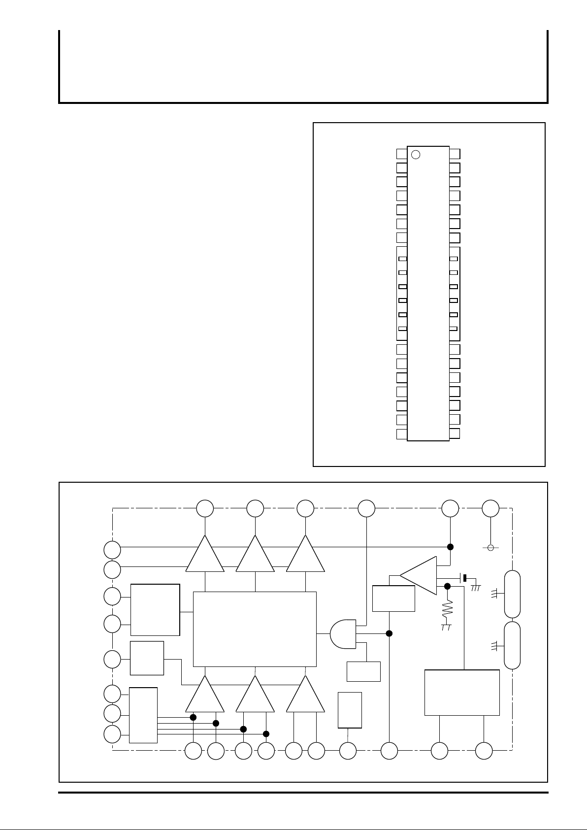
PIN CONFIGURATION (TOP VIEW)
N.C
S/S
RDS
FG
MODE2
MODE1
GND
VM
CC2
V
EC
ECR
VCC1
HB
N.C
1
2
3
4
CI
7
8
M56785FP
13
14
15 28
16
17
18
19
20
21
Outline 42P9R-A
N.C
42
W
41
V
40
U
39
RS
385
MODE3
376
MODE4
36
35
349
3310
3211
GND
3112
30
29
HwHw+
27
Hv-
26
Hv+
25
Hu-
24
Hu+
23
N.C
22
N.C: no connection
BLOCK DIAGRAM
15
VM
VCC2
16
FG
RDS
7
6
36
37
4
3
BRAKING
MODE
CHANGE
SENSE
FG
RDS
MODE1
MODE2
MODE4
MODE3
UV
39 40 41
120°
MATRIX
+ -+-+-
23
24 25 26 27 28
Hv+ Hv-
Hu-
Hu+
W
Hw+
Hw-
S/S
2 38
I / I
Converter
TSD
Hall
Bias
5
HB
CI
S
R
-
+
+
1720
EC ECR
Vref
V/I Converter
18
VCC1
19
8 to 14 29 to 35
GND
GND
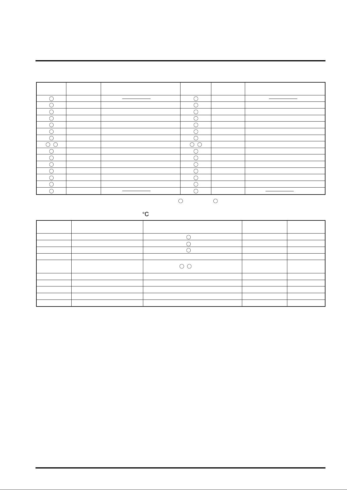
PIN DESCRIPTIO N
MITSUBISHI <CONTROL / DRIVER IC>
M56785FP
SPINDLE MOTOR DRIVER
Pin No. Symbol Function
1
2
3
4
5
6
7
N.C
S/S
RDS
FG
I
C
Reverse detected signal
Frequency generator output
Phase Compensation
MODE1 Reverse torque mode select 1
GND GNDGND GND
15
16
17
18
19
20
21
CC2 12V supply voltage MODE3 Automatic stop select
V
EC R
V
CC1 V5V supply voltage Motor drive output V
Bias for Hall SensorHB W Motor drive output W
N.C N.C
* Pull-up resistors (10kohm) are included in the circuits connected to pin [RDS] and pin[FG].
Pin No. Symbol Function
22
23
24
25
26
27
28
29 –358 –14
36
37
38
39
40
41
42
N.C
Hu+ Sensor amp. inputHu+Start / Stop
Hu- Hu- Sensor amp. input
Hv+ Hv+ Sensor amp. input
Hv- Hv- Sensor amp. input
Hw+ Hw+ Sensor amp. inputMODE2 Reverse torque mode select 2
Hw- Hw- Sensor amp. input
Hall amplifier sensitivity selectVM Motor supply voltage MODE4
SMotor speed control Motor current sense
U Motor drive output UECR The reference voltage for EC
43
ABSOLUTE MAXIMUM RATING (Ta=25 )
Symbol Rating UnitParameter Conditions
VCC2 12V supply voltage 16 pin 16
CC1 5V supply voltage V7.019 pin
V
Io Output current 1.5 ANote 1
Sensor amp.
Differential input range
Pt Power dissipation W1.2Free Air
Kθ
Thermal derating mW/˚CFree Air 9.6
Tj Junction temperature
Topr Operating temperature -20 +75
Tstg Storage temperature
23 –28
pins
16 V15 pinVM Motor supply voltage
150
–
–
V
V4.5VH(c)
˚C
˚C
˚C-40 +125
*Note1 ; The ICs must be operated within the Pt (power dissipation) or the area of safety operation
MITSUBISHI <CONTROL / DRIVER IC>
M56785FP
SPINDLE MOTOR DRIVER
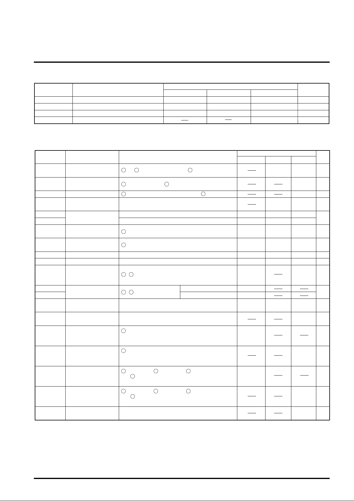
RECOMMENDED OPERATING CONDITIONS
Symbol Parameter
Min. Typ. Max.
5V Power supply V5.04.5 5.5VCC1
ELECTRICAL CHARACTERISTICS (VCC=5V, VCC2=12V, VM=12V, Ta=25˚C unless otherwise noted.)
Symbol Parameter
Icc1
Icc2
Sleep Mode Supply
current- 1
Sleep Mode Supply
current- 2
Supply current- 3Icc3 pin Input Current (EC=ECR=2.5V) [ pin High] 6.0 mA
Vsat Saturation voltage
ECdead-
ECdead+
ECR pin [3.3v DSP available] 1.65 V0.5 4.0
EC
Dead Zone Control
voltage dead zone
Reference voltage
Input range
Control voltage Input
range
15 16 2
and pin total Input Current ( pin low or open) 0 100
19 2
pin Input Current ( pin low or open) 500
19
Top and Bottom saturation voltage.
(Load current :500mA)
EC < ECR
EC > ECR
18
17
pin [3.3v DSP available] 0.5 4.0 V
Gio Control gain Io = Gio / Rsense [A/V] 0.3 V/V0.350.25
Vlim Control limit Ilim = Vlim / Rsense [A] 0.3 0.330.27 V
VH com
Hall sensor amp
common mode input
23 – 28
pins
range
VHmin1
VHmin2 MODE4=GND 35
VHb
Hall sensor amp.
input signal revel
Hall bias terminal
output voltage
23 – 28
pins
Load current (IHb) =10 mA. V0.85 1.20.6
Hall bias terminal sink
current
2
Von
Motor start voltage
pin input voltage when it starts up the motor.
*The IC is in the active condition.
*The hall bias is available.
2
Voff
Motor stop voltage
pin input voltage when it stops the motor.
*The IC is in the sleep condition.
*The hall bias is off.
7 6 37
V
ViL
iH
mode pin input high
voltage
mode pin input low
voltage
pin[MODE1], pin[MODE2], pin[MODE3]
36
and pin[MODE4] input voltage
when they are HIGH.
7 6 37
pin[MODE1], pin[MODE2], pin[MODE3]
36
and pin[MODE4] input voltage
when they are LOW.
V
OL
3pin[RDS],4pin[FG]
output low voltage
Io current = 1mA 0.5 V
Conditions
2
MODE4=OPEN or HIGH
Limits
12.04.5VCC2 12V Power supply 13.2 V
Limits
Min. Typ. Max.
1.2 1.9 V
-40 -21 0
+400 +21
1.65
1.2 4.5 V
50
30IHb
2.0
0.8
2.0
0.8
Unit
V12.04.5 13.2Motor Power supplyVM
mA700Io Output drive current
Unit
µA
µA
mV
mV
p-p
mA
V
V
V
V
MITSUBISHI <CONTROL / DRIVER IC>
M56785FP
SPINDLE MOTOR DRIVER
ELECTRICAL CHARACTERISTICS (VCC1=5V, VCC2=12V, VM=12V, Ta=25˚C Unless otherwise noted. )
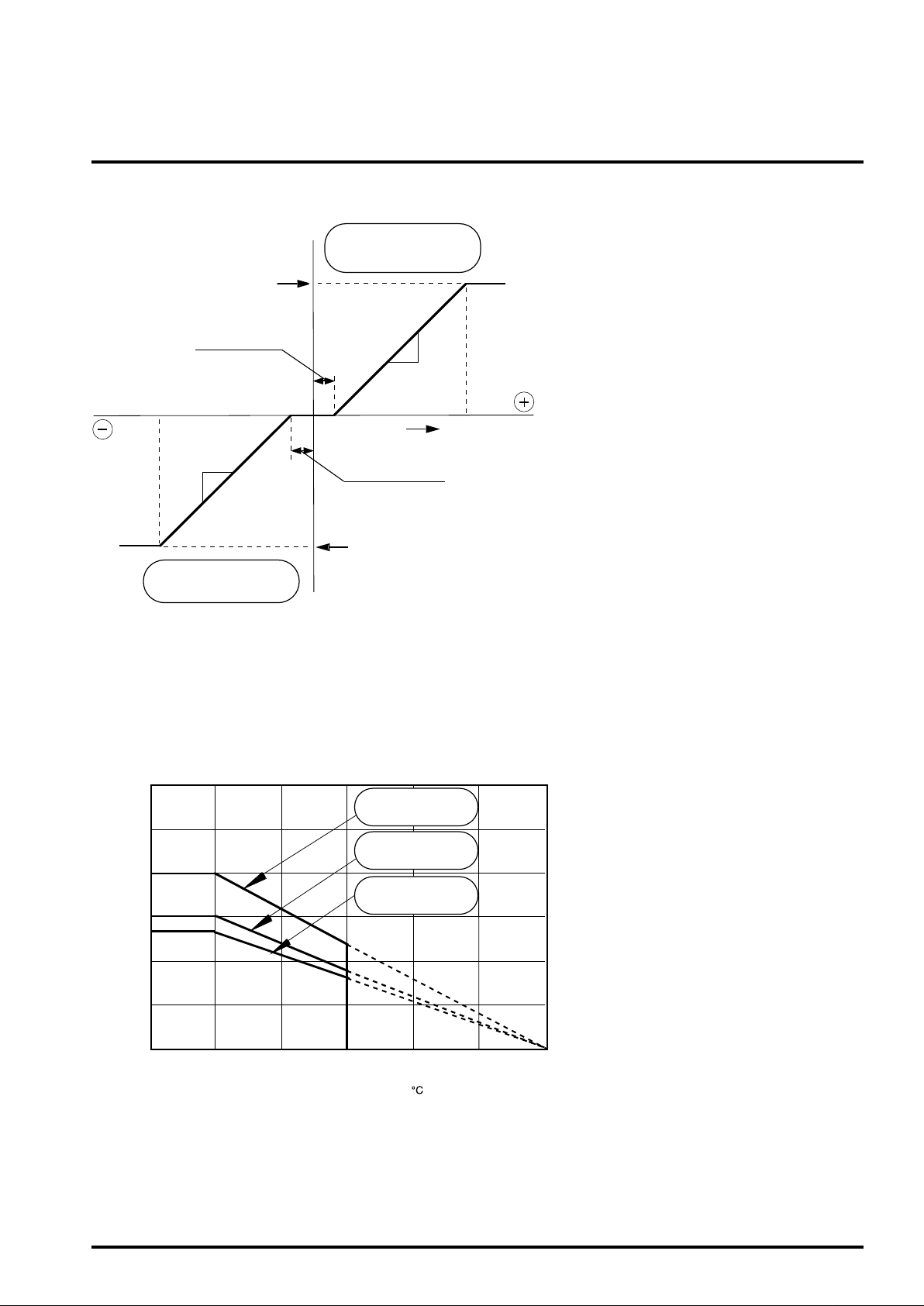
Reverse Torque
Current limit
0 – +40mV
0
0.6A/V
0 – -40mV
Current limit
Forward Torque
Figure 1. The characteristics of the control voltage
and motor current ( Torque ).
0.6A/V
The relationship between the EC-ECR (the difference
between EC<(control voltage> and ECR <reference
voltage> ) and the torque is shown in Figure 1.
The current gain is 0.6A/V (at sensing resistor :0.5ohm)
in both torque directions, and the dead zone is from
±0mV to ±40mV.
When the all short brake mode is selected, the coil
current under the reverse torque control depends on
the back emf. and the coil resistance.
EC - ECR
THERMAL DERATING
6.0
(W)
5.0
4.0
3.0
2.0
Power Dissipation (Pdp)
1.0
0 25 50 75 100 125
4.0W
using A-type board
3.0W
using B-type board
2.7W
using C-type board
Ambient Temperature Ta ( )
This IC's package is POWER-SSOP, so improving
the board on which the IC is mounted enables a
large power dissipation without a heat sink.
For example, using an 1 layer glass epoxy resin
board, the IC's power dissipation is 2.7W at least.
And it comes to 4.0W by using an improved 2 layer
board.
The information of the H, I, J type board is shown
in the board information.
150

HALL AMPLIFIER INPUT AND COMMUTATION
The relationship between the hall amplifier inputs voltage and the
motor current outputs is shown in Figure 2.
MITSUBISHI <CONTROL / DRIVER IC>
M56785FP
SPINDLE MOTOR DRIVER
Hu+Hv+Hw+
Hall
inputs
Output
current
U WV
V
SOURSE
UVWU
W
Figure 2.
HALL AMPLIFIER INPUT SENSITIVITY SELECT
MODE4
OPEN or HIGH GND
120 degree switching
120 degree
soft switching
** Io current
changes sharply.
SINK
Hall elements
W
V
V
W
U
U
FORWARD
EC<ECR
U
Outer loator
W
V
U
W
V
REVERSE
EC>ECR
Figure 3 shows the hall amplifier input sensitivity select function. You are
able to select a sensitivity of a hall amplifier out of two levels which is
suitable for the hall elements type.
If the output minimum level of the hall elements is lower than 50mVp-p,
please connect the MODE4 pin to external GND. In this case, the
output current changes shaply. If the output minimum level of the hall
elements is higher than 50mVp-p, please make the MODE4 pin open,
then the output current is commutated softly.
We recommend that the output level of the hall elements be set between
80mVp-p and 120mVp-p, and the MODE4 pin is an open.
The hallamp
minimum input voltage
The hallamp
minimum input voltage
is 50 mVp-p.
Figure 3.
SLEEP MODE FUNCTION
START / STOP ( pin)
LOW or OPEN HIGH
Motor Stop
Bias off
Hall-Bias of
Figure 4.
2
Motor on
Bias on
Hall-Bias on
is 35 mVp-p.
Figure 4 shows the sleep mode function. If the pin [S/S] is set to be
2
open or low, the motor drive outputs have high impedance and the motor
stops. Then, the IC bias current wil be a slight current (please refer to the
electrical characteristics), and the hall bias output will be cut off. When
the pin input is high, all the circuits will work.2

FORWARD AND REVERSE ROTATION DETECT
FUNCTION
Figure 5 shows the circuits and the functions of the forward and
reverse rotation detect .
The output of the RDS pin is determined by the signals of hall
inputs ( Hu+, Hu-, Hv+ and Hv- ) which indicate the direction of
rotation. When the motor is spinning forward, the RDS pin output
will be low. When the motor rotates reversely in stop mode, it will
be high.
The RDS pin is pulled-up to VCC1 by internal resistor (typ.10kohm).
MITSUBISHI <CONTROL / DRIVER IC>
M56785FP
SPINDLE MOTOR DRIVER
RDS FG
VCC1
RDS
FG
MODE3
CI
FORWARD
D
T
Q
High
Low
High
Low
VCC1
Q
Q
D
R
FG-amp
T
Hu+Hv+Hw+
EC-ECR
Comparator
Hysteresis
RDS
FG
+
-
+
-
REVERSE
D
T
Q
High
Low
High
Low
Hu+ Hu- Hv+ Hv- Hw+
Hall sensor-amp
Hv+
Hu+Hw+
Hw-
Figure 5.

MITSUBISHI <CONTROL / DRIVER IC>
M56785FP
SPINDLE MOTOR DRIVER
AUTOMATICALY STOP AFTER REVERSE
BRAKING FUNCTION
Figure 5 also shows the automaticaly stop (after the reverse
braking) circuit. Figure 6 is its function table which shows whether
the automaticaly stop function is on or off, and its state is
determined by MODE3 input.
When the MODE3 is open or high, the motor will stop rotating
automaticaly after the reverse braking.
When the MODE3 is low or connected to GND, the motor will
continue the reverse rotation. This function is useful for the case
that the system doesn't require the automaticaly stop function, and
in the system a motor receives a stop command from the outside
of this IC. For example, a µcom can detect the reverse rotation
from the RDS pin output, and can control all the torque of a motor.
So it can stop the motor outside this IC.
FG FUNCTION
Figure 5 also shows the circuits and the functions of the frequency
generator. The FG pin outputs the square pulse signal
synchronizing with the hall inputs [Hv+ and Hv-] timming .
The FG pin is pulled-up to V
10Kohm].
MODE3
OPEN or HIGH GND
AUTOMATIC
STOP
Figure 6.
CC1 by an internal resistor [typ.
UN-AUTOMATIC
(NON-STOP)
REVERSE TORQUE MODE SELECT FUNCTION
In the 4 times speed and the 6 times speed CDROM drive
system, the reverse braking style has been used for a
deceleration of the rotation speed. However, i n the CDROM
drive system above an 8 times speed, the motor current above
0.5A is needed, because a high speed access time are required
for motor driver ICs. If the reverse braking is used at 0.5A, the
IC junction temperature will be too much high, and the heat loss
of the IC will be large.
Therefore, this motor driver has the braking mode select
function (REVERSE BRAKING MODE and SHORT BRAKING
MODE). The breaking mode can be determined by the external
logic signals synchronizing with servo timing, and it can make a
heat loss of the IC smaller by adjusting the junction
temperature.
Figure 7 shows the reverse torque mode select function table. If
you want the former braking style (the reverse braking ), please
select only the REVERSE BRAKING mode [MODE1=LOW or
OPEN and MODE2=HIGH]. But the heat loss will be larger, and
sometimes external heat sink would be necessary.
If it is possible to get ports more than two from µcom, you can
flexibly control the four kinds of BRAKING MODE. So the heat
loss can be half as usual. For example, the REVERSE
BRAKING MODE is on under the CLV control, and the ALL
SHORT BRAKING MODE is for seeking. When the motor
should be stopped, the ALL SHORT BRAKING MODE or the
REVERSE BRAKING MODE is available.
If you can only get one port, you can control only the MODE2.
At this time, you can control the two kinds of BRAKING MODE
[commutated short or reverse] on condition that the MODE1 is
set to be LOW or OPEN.
BRAKING MODE (ECR < EC) SELECT FUNCTION TABLE
MODE1
MODE2
LOW
or
OPEN
HIGH
LOW or OPEN
COMMUTATED SHORT
BRAKING
REVERSE BRAKING
HIGH
ALL SHORT
BRAKING
OUTPUT OPEN
[only inertia]
Figure 7.

REVERSE TORQUE MODE SELECT FUNCTION
Figure 8 shows an example for the reverse torque mode select.
The CASE1 is an example for controlled REVERSE and
COMMUTATED SHORT BRAKING.
The CASE2 is an example for controlled REVERSE and ALL
SHORT BRAKING.
MITSUBISHI <CONTROL / DRIVER IC>
M56785FP
SPINDLE MOTOR DRIVER
CASE 1
FORWARD
Figure 8.
REVERSE AND COMMUTATED
SHORT BRAKING SELECT
EC PIN INPUT VOLTAGE [ECR VOLTAGE = 2.5V]
5.0V
3.0V
ECR 2.5V
2.0V
0V
HIGH
MODE2
LOW
MODE1
LOW
BRAKING
MODE
+1A
CURRENT
REVERSE
TORQUE
CURRENT
-1A
Commutated short
BRAKING
MOTOR CURRENT [ Rsense = 0.5 ohm ]
-60 0mA
REVERSE
BRAKING
+60 0mA
MOTOR
STOP
CASE 2
REVERSE AND ALL SHORT
BRAKING SELECT
EC PIN INPUT VOLTAGE [ECR VOLTAGE = 2.5V]
5.0V
3.0V
ECR 2.5V
2.0V
0V
HIGH
MODE2
LOW
MODE1
LOW
BRAKING
MODE
+1A
FORWARD
CURRENT
REVERSE
TORQUE
CURRENT
MOTOR CURRENT
-1A
ALL
SHORT
BRAKING
REVERSE
BRAKING
+60 0mA
-60 0mA
( Vbemf-Vd-Vsat ) / Ra
Vd ; diode voltage
Vsat ; npn transistor saturation voltage
Ra ; motor inner resistance
MOTOR
STOP

BASICALLY CHARACTERISTICS
This data is an example for typical sample.
Output saturation voltage and Load current Characteristics.
12.0
11.5
11.0
10.5
Output Voltage (V)
0.76
1.5
0.79
0.86
0.89
0.91
This device can use this
voltage value due to motor
drive.
(Condition Vcc2=Vm=12V, Vcc=5V)
0.98
MITSUBISHI <CONTROL / DRIVER IC>
M56785FP
SPINDLE MOTOR DRIVER
Top side
saturation
voltage
1.05
1.18
1.0
0.62
0.5
0.38
0.07
0
0.13
200 400 600 800 10000
0.25
0.32
Load current (mA)
0.49
Output saturation voltage and Load current Characteristics. (At bootstrap)
By taking advantage of bootstrap function, the output saturation
voltage can be lower.
5.0
4.5
4.0
3.5
0.06
0.12
0.23
0.29
0.35
This device can use this
voltage value due to motor
drive.
(Condition Vcc2=6V,Vm=5V,Vcc=5V)
0.47
0.62
0.76
Bottom side
saturation
voltage
1200
Top side
saturation
voltage
0.83
Output Voltage (V)
1.5
1.0
0.5
0.07
0
0.38
0.13
200 400 600 800 10000
0.25
0.32
Load current (mA)
0.49
0.62
0.76
Bottom side
saturation
voltage
1200

HB terminal voltage and Hall current characteristics.
1.6
1.4
1.2
1.0
0.85
0.8
0.6
HB terminal voltage (V)
0.4
MITSUBISHI <CONTROL / DRIVER IC>
M56785FP
SPINDLE MOTOR DRIVER
(Condition :Vcc=4.4V – 7V)
0.2
0
0
10
20 30
Hall current (mA)
40 50

APPLICATION CIRCUIT
Forward reverse
rotation signal
3
FG signal
37
4
MITSUBISHI <CONTROL / DRIVER IC>
M56785FP
SPINDLE MOTOR DRIVER
µcom control
BRAKING
MODE
SELECT
0 to 1.5
10µF
15
36
7
16
6
12V
Motor
power
supply
5V
Hall bias
resistor
HU
HV
HW
104
TSD
SENSE
CHANGE
MATRIX
120°
BRAKING
MODE
Converter
I / I
39
104
40 41
104
2 38
Start / Stop
104
RDS
FG
23 24 25 26 27 28
20
5
+- +- +-
Bias
Hall
Control
PWM1
Reference
PWM2
+
+
V/I Converter
1817
8 to 14 and 29 to 35
-
Vlim
Motor current sense resistor
0.5
19
5V
Power
Supply
10µF
 Loading...