Mitsubishi M56758FP Datasheet

MITSUBISHI <CONTROL / DRIVER IC>
)
M56758FP
5 CHANNEL ACTUATOR MOTOR DRIVER
DESCRIPTION
The M56758FP is a semiconductor integrated circuit designed for a
actuator driver used for MD, CD-audio, etc. This device can
function 5-channel-actuators by 1 chip due to include 5 channel
BTL drivers.
Sufficient output dynamic range can be obtained by low supply
voltage because saturation voltage of power output is low. All
channels include level shift circuit in order that output swings most
suitably although reference voltage of signal disposal system in
each system becomes 1.5V. And, differential PWM control is
possible since all channels are composed of Differential input
structure. Also, as this device includes general purpose OP amp, it
is suited to wide-ransing application. Further more, this devise is
able to power save since it includes mute circuit.
FEATURES
●3.3V DSP available
●Low saturation voltage.
(Typical 1.35V at load current 0.5A and no bootstrap condition.)
Absolute maximum rating of load current: CH1 – 5 500mA
A bootstrap function is available.
●There are two motor power supplies.
Vm1 CH1, 2 motor power supply-1
Vm2 CH3, 4, 5 motor power supply-2
●Built-in OP amp. for Regulator. (Enables Regulator structure by
using external PNP Tr. and resistor.)
●Flexible Input amp. setting.
Enables PWM control.
●Low cross-over distortion.
●Wide supply voltage range. (4.5V – 13.2V)
●Built-in Thermal protection.
●Built-in Mute circuit. (two systems)
MUTE1: CH1 – 4, MUTE2: CH5
APPLICATION
MD, CD-audio, CD-ROM, VCD, DVD etc.
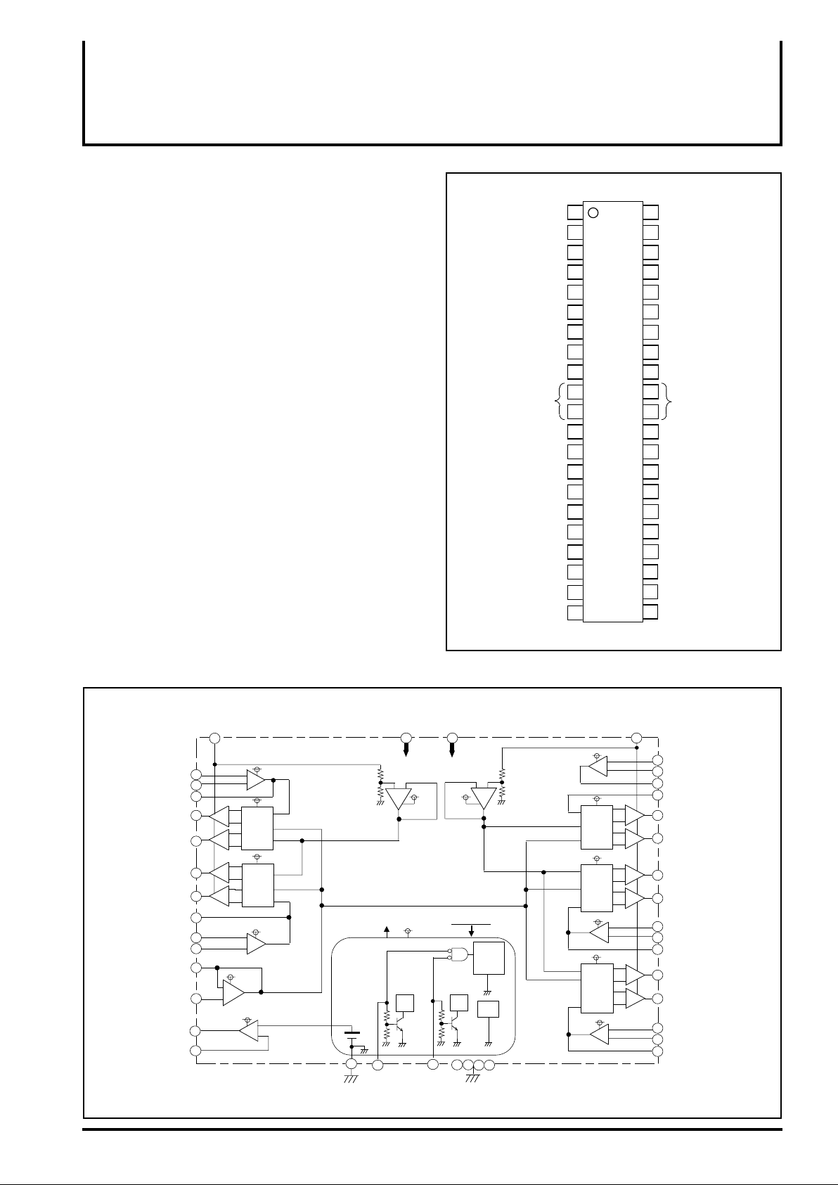
PIN CONFIGURATION(TOP VIEW
REG+
REGB
IN1+
V
BS1
Vm1
IN1-
OUT1
VM1-
VM1+
GND
VM2+
VM2-
OUT2
IN2-
IN2+
MUTE1
MUTE2
SS.GND
V
REF
VREFO
1
2
3
4
7
8
13
14
15 28
16
17
18
19
20
21
Outline 42P2R-D
42
41
40
39
385
376
36
35
349
M56758FP
3310
3211
3112
30
29
27
26
25
24
23
22
CH3IN
OUT3
IN3V
BS2
Vm2
IN3+
N.C
VM3VM3+
GND
VM4+
VM4VM5+
VM5OUT5
IN5IN5+
IN4+
IN4OUT4
N.C: no connection
BLOCK DIAGRAM
IN1+
IN1-
OUT1
VM1(+)
VM1(-)
VM2(+)
VM2(-)
OUT2
IN2-
IN2+
VREFO
VREF
REGB
REG+
Vm1
VREG
+
-
+
+
-
+
-
VBS2
+
VBS1
V
+
-
CH1
×5
CH2
×5
-
+
REF
-
+
E1
E2
VBS1
VBS1
VBS1
VBS1
1.25V
SS.GND
R
R
Vrefm1
BIAS
MUTE1
VBS1
+
-
Low,Open
MUTE ON
1 – 4
CH
VBS2
Vm1 Vm2
VBS1
MUTE2
+
-
Vrefm2
VREFO
Hi: Sleep
SLEEP
5CH
TSD
GND (4PIN)
Vm2
VBS2
-
VBS2
E3
+
R
R
CH3
-
×8
+
VBS2
CH4
-
×8
+
VBS2
-
+
E4
VBS2
CH5
×8
+
VBS2
-
+
E5
IN3IN3+
OUT3
CH3IN
+
-
VM3(+)
VM3(-)
+
-
VM4(+)
VM4(-)
IN4IN4+
OUT4
+
-
VM5(+)
VM5(-)
IN5IN5+
OUT5

)
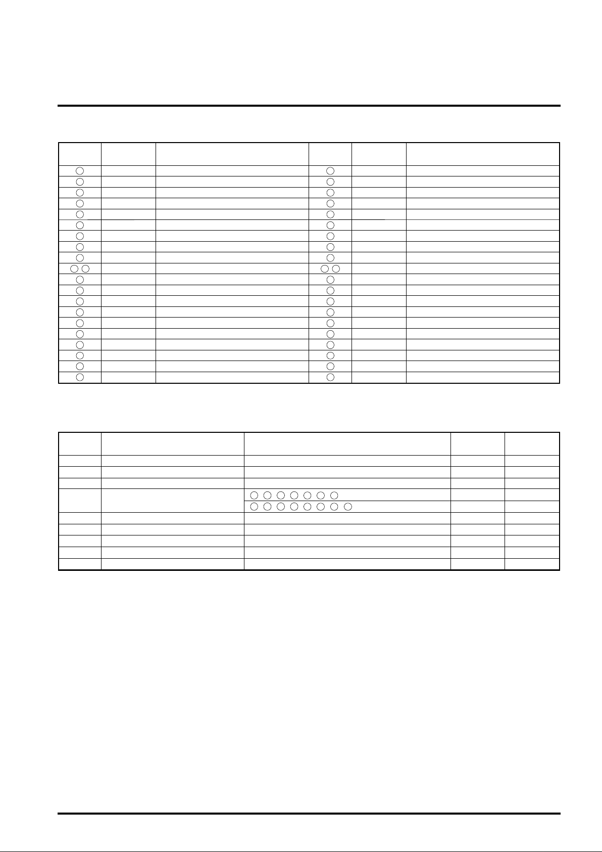
PIN FUNCTION
MITSUBISHI <CONTROL / DRIVER IC>
M56758FP
5 CHANNEL ACTUATOR MOTOR DRIVER
Pin No.
1
2
3
4
5
6
7
8
9
1110
,
12
13
14
15
16
17
18
19
20
21
Symbol Function
REG+
REGB
IN1+
BS1
V
Vm1
IN1OUT1
VM1(-)
VM1(+)
GND
VM2(+)
VM2(-)
OUT2
IN2IN2+
MUTE1
MUTE2
SS.GND
REF
V
VREFO
Regulator voltage setting resistor
Regulator PNP base connect
E1 amplifier non-inverted input
Bootstrap power supply
Motor power supply
E1 amplifier inverted input
E1 amplifier output
CH1 inverted output
CH1 non-inverted output
Motor GND
CH2 non-inverted output
CH2 inverted output
E2 amplifier output
E2 amplifier inverted input
E2 amplifier non-inverted input
CH1 – 4 mute
CH5 mute
Small signal GND
Reference voltage input
Reference voltage output
Pin No.
42
41
40
39
38
37
36
35
34
3332
,
31
30
29
28
27
26
25
24
23
22
Symbol
CH3IN
OUT3
IN3-
BS2
V
Vm2
IN3+
N.C
VM3(-)
VM3(+)
GND
VM4(+)
VM4(-)
VM5(+)
VM5(-)
OUT5
IN5IN5+
IN4+
IN4OUT4
CH3 non-inverted input
E3 amplifier output
E3 amplifier inverted input
Bootstrap power supply
Motor power supply
E3 amplifier non-inverted input
N.C
CH3 inverted output
CH3 non-inverted output
Motor GND
CH4 non-inverted output
CH4 inverted output
CH5 non-inverted output
CH5 inverted output
E5 amplifier output
E5 amplifier inverted input
E5 amplifier non-inverted input
E4 amplifier non-inverted input
E4 amplifier inverted input
E4 amplifier output
ABSOLUTE MAXIMUM RATING(Ta = 25°C
Symbol Conditions UnitParameter
BS Bootstrap power supply VBS power supply 15
V
Vm
Io
Vin
Pt
Kθ
Tj
Topr
Tstg
Maximum input voltage
of terminals
Operating temperature
Storage temperature
3 6 15 16 17 18 20
1 23 24 25 26 37 40 42
, , , , , , , PIN
Function
Rating
BS1
0 – VBS2
1.2
9.6
150
-20 – +75
-40 – +150
V
VMotor power supply Vm power supply 15
mAOutput Current 500
V, , , , , , PIN 0 – V
V
WPower dissipation Free Air
mW/°CThermal derating Free Air
°CJunction temperature
°C
°C

MITSUBISHI <CONTROL / DRIVER IC>
)
5 CHANNEL ACTUATOR MOTOR DRIVER
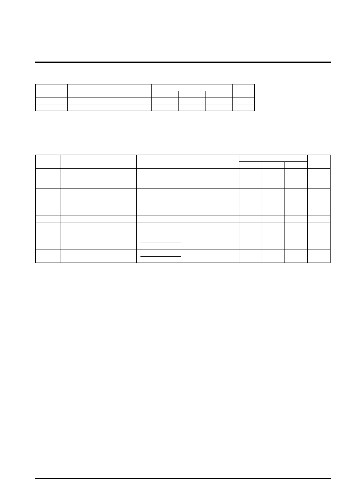
RECOMMENDED OPERATING CONDITIONS
Symbol
Vm1, Vm2
V
BS1,VBS2
Parameter
Motor power supply
Bootstrap power supply
Min.
Limits
Typ.
5.0
Vm* + 1.0
Max.
Units
V
V
ELECTRICAL CHARACTERISTICS(Ta = 25°C, VBS = Vm = 5V unless otherwise noted
Symbol Conditions UnitsParameter
CC1 Supply current - 1 VBS1, VBS2, Vm1, Vm2 current
I
BS1,VBS2,Vm1,Vm2 current at Sleep Mode
ICC2
Vsat1
Voff1
Voff2
Voff3
Voff4
Voff5
Gain1
Gain2
Supply current - 2
Ch1 – 5 Saturation voltage
CH1 output offset voltage
CH2 output offset voltage
CH3 output offset voltage
CH4 output offset voltage
CH5 output offset voltage
CH1 Voltage Gain between
input and output
CH2 Voltage Gain between
input and output
V
(MUTE1 and MUTE2 are inputted to Low).
Top and Bottom saturation voltage.
Load current 0.5A and no bootstrap.
VREFO = OUT1 = 1.5V
V
REFO = OUT2 = 1.5V
V
REFO = CH3IN = 1.5V
V
REFO = OUT4 = 1.5V
V
REFO = OUT5 = 1.5V
{VM1(+) – VM1(-)}
(OUT1 – VREFO)
{VM2(+) – VM2(-)}
(OUT2 – VREFO)
Min.
—
—
—
-41
-41
-47
-47
-47
4.5
4.5
M56758FP
Limits
Typ.
35
1.3
1.35
—
—
—
—
—
5
5
Max.
50
2.2
1.9
41
41
47
47
47
5.5
5.5
mA
mA
V
mV
mV
mV
mV
mV
V/V
V/V
 Loading...