

MITSUBISHI <CONTROL / DRIVER IC>
M56755AFP
SPINDLE MOTOR DRIVER
DESCRIPTION
The M56755AFP is a semiconductor integrated circuit designed for
a single chip controller for CD-ROM spindle motor.
M56755AFP has a both (forward and reverse) motor torque control
by the motor speed control terminal.
M56755AFP has the several braking mode that an user can flexibly
select in order to generate the reverse torque. Also, this device
includes a bias circuit for Hall Sensor, a current limit circuit and a
thermal shut down function.
FEATURES
●3.3V DSP available.
●The supply voltage with wide range.
(4.5V to 13.2V)
●High motor drive current (1.2A).
●Motor current control for the both motor torque is possible.
●Reverse torque mode select [SHORT BRAKING, etc]
●Sleep mode
●Hall amplifier sensitivity select
●Automatic stop select (with reverse detected signal pin)
APPLICATION
Above 8 times speed CD-ROM, DVD, DVD-ROM etc.
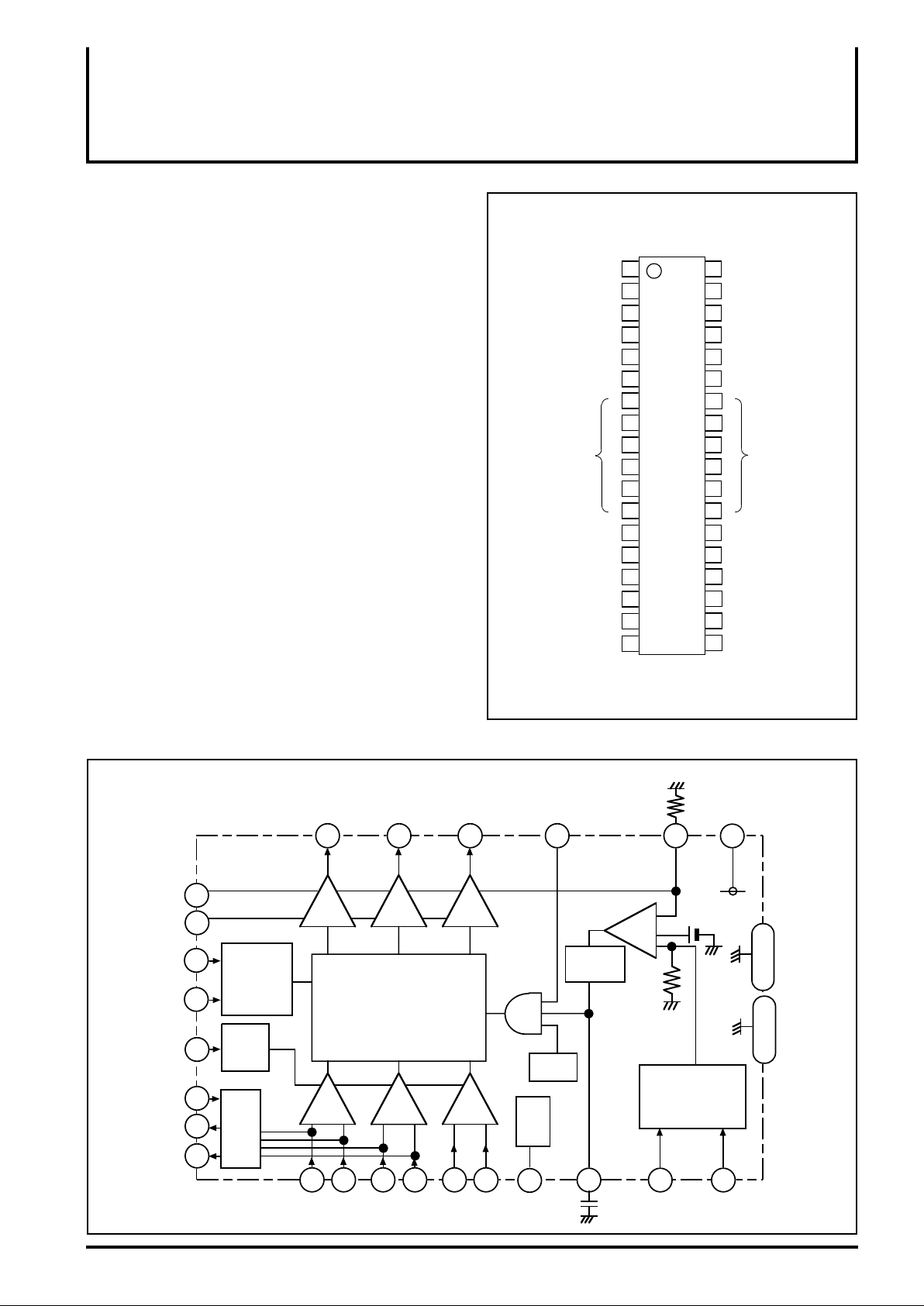
PIN CONFIGURATION (TOP VIEW)
1
S/S
2
RDS
3
FG
4
I
C
MODE2
MODE1
7
8
GND GND
13
M
V
14
VCC2
15 22
EC
16
ECR
17
CC1
V
18
HB
36
35
34
33
325
316
30
M56755AFP
29
289
2710
2611
2512
24
23
21
20
19
W
V
U
S
R
MODE3
MODE4
HwHw+
HvHv+
HuHu+
BLOCK DIAGRAM
VM
13
VCC2
14
MODE1
MODE2
MODE4
MODE3
FG
RDS
6
5
31
32
3
2
BRAKING
MODE
CHANGE
SENSE
FG
RDS
W
34 35 36
120°
MATRIX
+- +- +-
19 20 21 22 23 24
Hu+ Hu- Hv+ Hv- Hw+ Hw-
S/S
1 1733
I / I
Converter
TSD
Hall
Bias
18
HB
4
I
C
Outline 36P2R-D
RSVU
-
+
+
15 16
EC
Vref
V/I Converter
VCC1
7 to 12
GND
25 to 30
GND
ECR
PIN FUNCTION
(c)
j
MITSUBISHI <CONTROL / DRIVER IC>
M56755AFP
SPINDLE MOTOR DRIVER
Symbol FunctionPin No. Pin No.
1
S/S
2
RDS
3
FG
4
C
I
5
MODE2
6
MODE1
7 12
–
13
14
15
16
17
18
*The pin[RDS] and pin[FG] are with pull-up resistor (10kohm).
GND
V
M
VCC2
EC
ECR
V
CC1
HB
2 3
Start/ Stop
Reverse detected signal
Frequency generator output
Phase Compensation
Reverse torque mode select 2
Reverse torque mode select 1
GND
Motor supply voltage
12V supply voltage
Motor speed control
The reference voltage for EC
5V supply voltage
Bias for Hall Sensor
19
20
21
22
23
24
25 30
–
31
32
33
34
35
36
Symbol
Hu+
HuHv+
HvHw+
HwGND
MODE4
MODE3
R
S
U
V
W
Hu+ Sensor amp. input
Hu- Sensor amp. input
Hv+ Sensor amp. input
Hv- Sensor amp. input
Hw+ Sensor amp. input
Hw- Sensor amp. input
GND
Hall amplifier sensitivity select
Automatic stop select
Motor current sense
Motor drive output U
Motor drive output V
Motor drive output W
ABSOLUTE MAXIMUM RATING (Ta = 25°C)
Symbol Conditions UnitsParameter
M Motor supply voltage pin maximum input voltage 16
V
VCC2
V
CC1
Io
VH
Pt
Kθ
T
Topr
Tstg
Output current
Sensor amp.
Differential input range
Power dissipation
Thermal derating
Junction temperature
Operating temperature
Storage temperature
*Note1; There is no overing Pt (power dissipation) or the area of safety operation.
13
14
17
pin maximum input voltage
*Note 1
19 24
– pins
Free Air
Function
Rating
4.5
1.2
9.6
150
-20 – +75
-40 – +125
V
V12V supply voltage pin maximum input voltage 16
V5V supply voltage 7.0
A1.5
V
WFree Air
mW/°C
°C
°C
°C
MITSUBISHI <CONTROL / DRIVER IC>
[
]
]
µAµ
M56755AFP
SPINDLE MOTOR DRIVER
RECOMMENDED OPERATING CONDITIONS
Symbol
CC1 5V Power supply
V
CC2 V
VM
Io
12V Power supplyV
Motor Power supply
Output drive current
Parameter
Min.
4.5
4.5
4.5
—
Limits
Typ.
5.0
12.0
12.0
—
Max.
5.5
13.2
13.2
700
ELECTRICAL CHARACTERISTICS (VCC = 5V, VCC2 = 12V ,VM = 12V, Ta = 25°C unless otherwise noted.)
Symbol Conditions UnitsParameter
CC1 Sleep Mode Supply current - 1 and pin total Input Current [ pin lo or open]
I
ICC2
ICC3
Vsat
ECdead-
ECdead+
ECR
EC
Gio
Vlim
VH com
VHmin1
VHmin2
Sleep Mode Supply current - 2
Supply current - 3
Saturation voltage
Control voltage dead zone
Reference voltage Input range
Control voltage Input range
Control gain
Control limit
Hall sensor amp common
mode input range
Hall sensor amp.
input signal revel
13 14 1
17
pin Input Current [ pin lo or open]
17
pin Input Current (EC = ECR = 2.5V) [ pin Hi]
1
Top and Bottom saturation voltage
Load current 500mA
EC < ECR
EC > ECR
pin Input voltage range [3.3V DSP available]
16
15
pin Input voltage range [3.3V DSP available]
Io = Gio / Rsense
A/V
Ilim = Vlim / Rsense [A
– pins input range
19 24
19 24
– pins input signal
MODE4 = open
MODE4 = GND
Units
V
V
mA
Limits
Min.
—
—
1
—
—
-40
0
0.5
0.5
0.25
0.27
1.2
50
35
Typ.
0
—
—
1.2
-21
+21
1.65
1.65
0.3
0.3
—
—
—
Max.
100
500
6.0
1.9
0
+40
4.0
4.0
0.35
0.33
4.5
—
—
mVp-p
A
mA
V
mV
V
V
V/V
V
V

MITSUBISHI <CONTROL / DRIVER IC>
y
q
M56755AFP
SPINDLE MOTOR DRIVER
ELECTRICAL CHARACTERISTICS (VCC = 5V, VCC2 = 12V ,VM = 12V, Ta = 25°C unless otherwise noted.)
mbol Conditions
S
VHb
Hall bias terminal output
voltage
Parameter
Load current (IHb) 10mA.
Min. Typ. Max.
0.6
Limits
0.85
Units
1.2
V
IHb
Von
Hall bias terminal sink current
Motor start voltage
1
pin input voltage when makes the motor start up.
*The ICs will be the active condition.
*The hall bias will be available.
1
pin input voltage when makes the motor stop.
Voff
Motor stop voltage
*The ICs will be the sleep condition.
*The hall bias will be off.
6 5 32
pin [MODE1], pin [MODE2], pin [MODE3]
31
H
Vi
mode pin input high voltage
and pin [MODE4] input voltage
when makes high level.
6 5 32
pin [MODE1], pin [MODE2], pin [MODE3]
ViL
mode pin input low voltage
31
and pin [MODE4] input voltage
when makes low level.
2 3
VOL
pin[RDS], pin[FG] output
low voltage
at Io current = 1mA
ELECTRICAL CHARACTERISTICS
(VCC=5V, VM=12V, Ta=25°C Unless otherwise noted.)
Reverse Torque
Current limit
—
2.0
—
2.0
—
—
—
—
—
—
—
—
30
—
0.8
—
0.8
0.5
mA
V
V
V
V
V
0 – +40mV
0.6A/V
0
EC - ECR
The relationship between the EC (control
voltage), ECR (reference voltage) and the
torque is as shown in Figure 1. The current
gain is 0.6A/V (at sensing resistor: 0.5ohm) in
the both torques and a dead zone is ±0mV to
0.6A/V
0 – -40mV
±40mV.
Current limit
Forward Tor
ue
Figure 1. The characteristics of the control voltage and motor current (Torque).

HALL AMPLIFIER INPUT AND COMMUTATION
The relationship between the hall amplifier inputs voltage and the
motor current outputs is as shown in Figure 2.
MITSUBISHI <CONTROL / DRIVER IC>
M56755AFP
SPINDLE MOTOR DRIVER
Hu+Hv+Hw+ Hall elements
Hall
inputs
Output
current
V
U
W
V
UVW WU
Figure 2.
HALL AMPLIFIER INPUT SENSITIVITY SELECT
MODE4
OPEN or HIGH GND
120 degree
soft switching
The hall amp
input voltage
minimum is
50mVp-p.
120 degree switching
** Io current
will be shape.
The hall amp
input voltage
minimum is
35mVp-p.
Figure 3.
SOURSE
SINK
U
V
W
U
W
V
W
U
FORWARD
EC < ECR
V
U
W
V
Outer loator
REVERSE
EC > ECR
Figure 3 shows the hall amplifier input sensitivity select function.
An user is able to select the sensitivity of a hall amplifier to match
with the hall elements type.
If the output minimum level of a hall elements is a low level as
below 50mVp-p, please connect the MODE4 to GND at external.
In this case, the output current will be shape. If the output minimum
level of a hall elements is more higher than 50mVp-p, please make
the MODE4 to open, then the output current will be commutated
softly.
We recommend that the output level of a hall element is used for
80mVp-p to 120mVp-p and the MODE4 is made to open.
SLEEP MODE FUNCTION
START / STOP
LOW or OPEN HIGH
Motor Stop
Bias off
Hall-Bias off
Motor on
Bias on
Hall-Bias on
Figure 4.
Figure 4 shows the sleep mode function. If the pin [S/S] is set to
1
open or low, the current output will be high impedance and then
the motor will be stop. Also, the IC bias current wil be a slight
current (please make reference the electrical characteristics). At
the same time, the hall bias output will be cut off. When the pin
1
goes high, the all of circuits will be available.

MITSUBISHI <CONTROL / DRIVER IC>
NG
s
M56755AFP
SPINDLE MOTOR DRIVER
FORWARD AND REVERSE ROTATION DETECT
Figure 5 shows the circuits and function of the forward and reverse
rotation detect.
The RDS is the output signal pin that detected by the signal of hall
inputs (Hu+, Hu-, Hv+ and Hv-). The RDS pin is pulled-up to VCC1
by internal resistor (typ. 10kohm). When the motor is spinning at
forward, the RDS pin output will be a low level. When the rotation
of motor is reversed at stop mode, it will be a high level.
AUTOMATICALY S TOP AFTER REVERSE BRAK-I
Figure 5 shows the automaticaly stop circuits after the reverse
braking, too. Figure 6 shows its function table. The MODE3 is the
input pin in order to be selected either the automaticaly stop or
non-stop. When the MODE3 is open, the motor rotation will be
stopped automaticaly after the reverse braking in order to make
stop the motor. When the MODE3 is connected to GND, the motor
RDS FG
VCC1
MODE3
CC1
V
FG-amp
CI
+
-
will continue the reversed rotation. This mode [MODE3=GND] is
available for the case that an user hope to control the motor
stopping at external.
FG FUNCTION
Figure 5 shows the circuits and function of the frequency
generator, too. The FG is the pin that output the signal synchronize
with the hall inputs [Hv+ and Hv-] timming.
The FG pin is pulled-up to VCC1 by internal resistor [typ. 10Kohm].
MODE3
OPEN or HIGH
AUTOMATIC
STOP
GND
UN-AUTOMATIC
(NON-STOP)
Figure 6 .
Hu+ Hu- Hv+ Hv- Hw+ Hw-
.
Figure 5.
FORWARD
High
RDS
Low
High
FG
Low
Q
TDQ
R
EC-ECR
Hu+
Hv+Hw+
D
T
Q
+
-
REVERSE
Comparator
H
ystelesi
RDS
FG
D
T
Q
High
Low
High
Low
Hw+
Hall sensor-amp
Hu+
Hv+

MITSUBISHI <CONTROL / DRIVER IC>
)
G
G
3.0
5.0V0
O
O
600mA(Vbe
a
ode voltage
age
ce
3.0
5.0V0
M56755AFP
SPINDLE MOTOR DRIVER
REVERSE TORQUE MODE SELECT FUNCTION
At the 4 times speed and the 6 times speed CDROM drive system,
the reverse braking style has been used for the reverse torque.
However, at the 8 times speed CDROM drive system, the motor
current will be needed above 0.7A, if an user of driver IC require a
high speed access time.
If the reverse braking is used at 0.7A, the IC junction temperature
will be too much high.
Therefore, MITSUBISHI new motor driver has the braking mode
select function. This mode select function is available in order to
control flexibly in match with the situation of junction temperature.
Figure 7 shows the reverse torque mode select function table.
BRAKING MODE (ECR < EC) SELECT FUNCTION TABLE
MODE1
LOW or OPEN
MODE2
LOW
or
OPEN
HIGH
COMMUTATED SHORT
BRAKIN
REVERSE BRAKING
SHORT BRAKING (2
ALL SHORT
BRAKIN
OUTPUT OPEN
[only inertia]
Figure 7.
If you hope original (the reverse braking) style, please only select
REVERSE BRAKING mode [MODE1 = LOW or OPEN and
MODE2 = HIGH] at external. If it is possible to get two more port
from µcom, you can flexibly control the four kinds of BRAKING
MODE. If you can only get one more port, you can control only the
MODE2. Then, you can control the two kinds of BRAKING MODE
[commutated short or reverse] under the MODE1 is set to LOW or
OPEN.
Figure 8 shows an example for the reverse torque
mode select.
HIGH
The CASE1 is an controlling example for REVERSE
and COMMUTATED SHORT BRAKING.
The CASE2 is an controlling example for REVERSE
and ALL SHORT BRAKING.
CASE 1
REVERSE AND COMMUTATED SHORT
BRAKING SELECT
EC PIN INPUT VOLTAGE [ECR VOLTAGE = 2.5V]
V
2.5V
ECR
2.0V
V
HIGH
MODE2
W
L
MODE1
LOW
BRAKING
MODE
+1A
FORWARD
CURRENT
REVERSE
TORQUE
CURRENT
-1A
Commutated short
BRAKING
MOTOR CURRENT [ Rsense = 0.5 ohm]
-600mA
Figure 8.
REVERSE
BRAKING
+600mA
MOTOR
STOP
2.5V
ECR
2.0V
HIGH
MODE2
L
MODE1
LOW
BRAKING
MODE
+1A
FORWARD
CURRENT
REVERSE
TORQUE
CURRENT
CASE 2
REVERSE AND ALL SHORT BRAKING SELECT
EC PIN INPUT VOLTAGE [ECR VOLTAGE = 2.5V]
V
V
W
ALL
SHORT
BRAKING
MOTOR CURRENT
-1A
mf-Vd-Vsat) / R
Vsat ; npn transistor saturation volt
REVERSE
BRAKING
+600mA
-
Vd ; di
Ra ; motor inner resistan
MOTOR
STOP

MITSUBISHI <CONTROL / DRIVER IC>
)
)
BASICALLY CHARACTERISTICS This data is an example for typical sample.
Output saturation voltage and Load current Characteristics. (Condition Vcc2 = Vm = 12V, Vcc = 5V)
12.0
M56755AFP
SPINDLE MOTOR DRIVER
11.5
11.0
10.5
Output Voltage (V)
1.5
1.0
0.5
0.76
0.07
0
0
Output saturation voltage and Load current Characteristics. (At bootstrap)
If you use a bootstrap as below,it is possible to make low the output
saturation voltage. (Condition Vcc2=6V,Vm=5V,Vcc=5V)
0.79
200 400 600 800 1000
0.13
0.86
0.25
0.89
0.32
Load current (mA
0.91
This device can use this voltage value
due to motor drive.
0.38
0.98
0.49
1.05
0.62
Top side
saturation voltage
1.18
0.76
Bottom side
saturation voltage
1200
5.0
4.5
4.0
3.5
Output Voltage (V)
1.5
1.0
0.5
0.06
0.07
0
0
0.29
0.12
0.23
0.25
0.13
0.32
200 400 600 800 1000
Load current (mA
0.35
This device can use this voltage value
due to motor drive.
0.38
0.47
0.49
0.62
0.62
0.83
0.76
1200
Top side
saturation voltage
Bottom side
saturation voltage

MITSUBISHI <CONTROL / DRIVER IC>
(mA)
)
(W)
SPINDLE MOTOR DRIVER
HB terminal voltage and Hall current characteristics. (Condition : Vcc = 4.4V – 7V)
1.6
1.4
1.2
1.0
0.85
0.8
0.6
HB terminal voltage (V)
0.4
M56755AFP
0.2
0
0
THERMAL DERATING
6.0
5.0
4.5
4.0
3.0
2.0
Power Dissipation (Pdp)
1.2
1.0
0 25 50 75 100 125 150
10
20 30
Hall current
With infinite heatsink
Without heatsink
Ambient Temperature (Ta
40 50
(°C)

APPLICATION CIRCUIT
µ
MITSUBISHI <CONTROL / DRIVER IC>
M56755AFP
SPINDLE MOTOR DRIVER
5V
Hall bias
resistance
Hu
Hv
Hw
Forward
reverse
rotation
signal
2
19
20
21
22 23 24
FG
signal
3
FG
RDS
+-
+-
+-
com control
BRAKING
MODE
SELECT
0 to 1.5
10uF
13
32
31
SENSE
6
CHANGE
MATRIX
120°
BRAKING
MODE
14
5
34
104
35
104
36
12V
Motor
power
supply
104
Control
PWM1
Reference
PWM2
104
18
4
15
16
Bias
Hall
V/I Converter
TSD
Converter
I / I
+
7 to 12 and 25 to 30
+
-
Vlim
1
1733
Start / Stop
Motor current sense resistor
0.5
10uF
5V
Power
Supply
 Loading...