MITSUBISHI <CONTROL / DRIVER IC>
)
M56754SP
4-CHANNEL ACTUATOR MOTOR DRIVER
DESCRIPTION
The M56754SP is a semiconductor IC developed as the motor
driver used for CD-ROM and CD player.
This circuit includes 4-Channel BTL Driver that is able to drive four
actuator with one IC.
FEATURES
● Low Output saturation voltage(typ:1.35V at 0.5A)
● Large operating supply voltage range(4.5–13.2V)
● Minimum Crossover distortion
● Built-in general operational amplifier
APPLICATION
CD-ROM, CD player
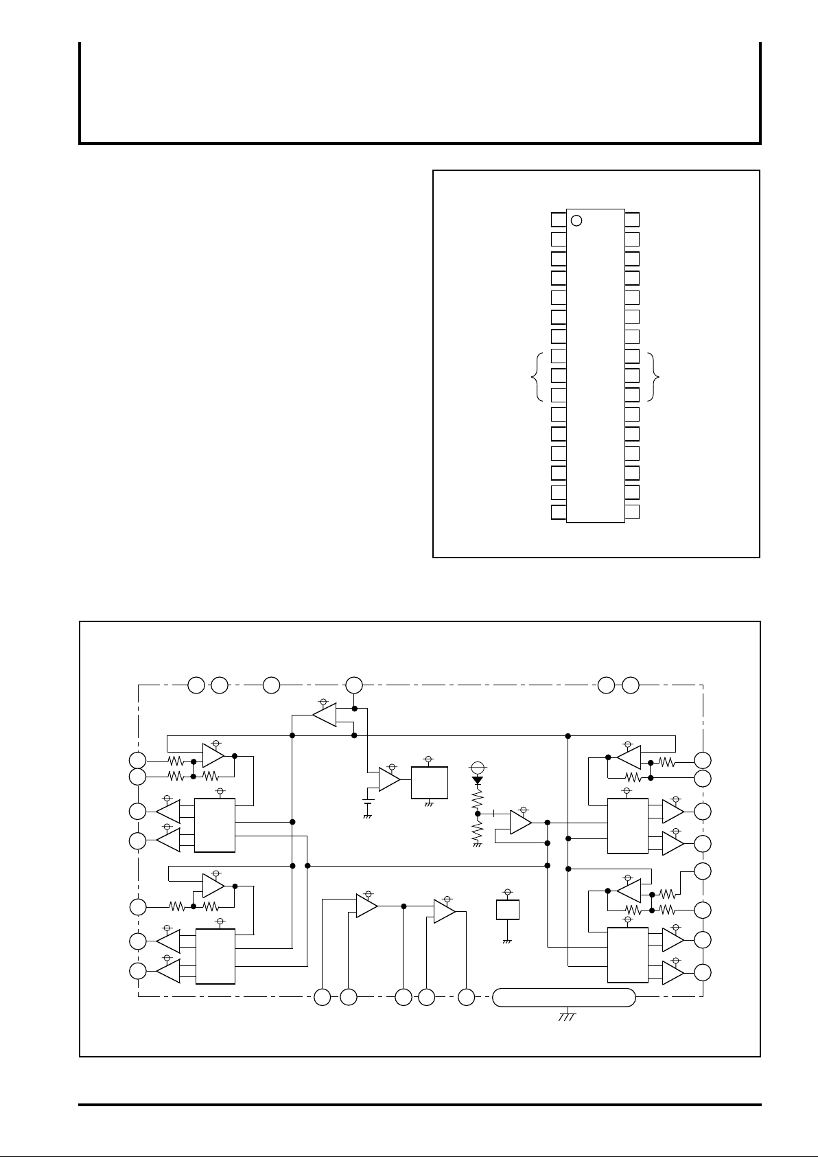
PIN CONFIGURATION(TOP VIEW
V
Vbs1
Vm1
Vctl1L
Vctl1H
VM1(-)
VM1(+)
GND
VM2(+)
VM2(-)
Vctl2
A1+
A1out
1
CC
2
3
4
6
7
8
10
12
13
14
A1-
15 18
16 17
Outline 32P4B
32
31
30
29
285
27
M56754SP
26
25
249
23
2211
21
20
19
Vref
Vctl4(2)
Vbs2
Vm2
Vctl4(1)
VM4(+)
VM4(-)
GND
VM3(+)
VM3(-)
Vctl3H
Vctl3L
A2out
A2-
BLOCK DIAGRAM
Vm1 Vbs1
3 2
Vctl1L
4
5
Vctl1H
Vm1
VM1(+)
VM1(-)
Vctl2
VM2(+)
VM2(-)
+
7
-
Vm1
-
6
+
13
Vm1
+
11
12
Vm1
-
-
+
+
-
CH1
+
-
CH2
Vbs1
Vbs1
Vbs1
Vbs1
Vbs2
30
Vbs2
Vbs2
Vbs2
Vbs2
Vm2
CH4
CH3
29
+
-
+
-
-
+
+
-
+
-
-
+
Vm2
Vm2
Vm2
Vm2
31
28
27
26
19
20
22
21
Vctl4(2)
Vctl4(1)
VM4(+)
VM4(-)
Vctl3(L)
Vctl3(H)
VM3(+)
VM3(-)
V
CC
1
V
Vref
32
CC
+
-
Vrefs
VCC
VCC
VCC
+
Current
-
Bias
+
-
V
161514
17
Vm2
Vrefm
CC
+
-
VCC
18
A2outA2-A1outA1-A1+
Vbs2
+
-
TSD
8 , 9 ,10, 23 ,24 ,25
GND(6PIN)

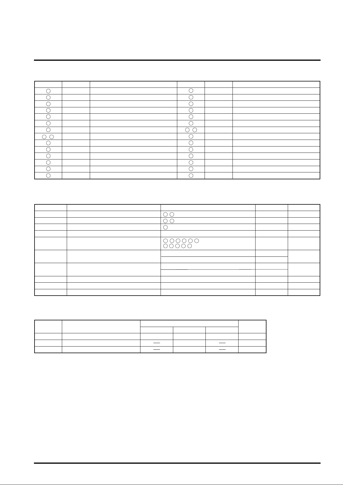
PIN DESCRIPTIONS
Symbol SymbolPin No. Function Pin No. Function
1
V
CC
2
Vbs1
3
Vm1
4
Vctl1L
5
Vctl1H
6
VM1(-) CH1 amp. inverted output terminal
7
8 –10
11
12 28
13
14 30
15
16
VM2(+) CH2 amp. non-inverted output terminal
VM2(-) CH2 amp. inverted output terminal
Vctl2 CH2 amp. input terminal
A1+ OP amp. 1 non-inverted input terminal
A1- OP amp. 1 inverted input terminal
A1out OP amp. 1 output terminal
5V power supply
Boot strap power supply terminal 1
Motor power supply terminal 1
CH1 amp. L gain input terminal
CH1 amp. H gain input terminal
MITSUBISHI <CONTROL / DRIVER IC>
M56754SP
4-CHANNEL ACTUATOR MOTOR DRIVER
17
18
19
20
21
22
23 – 25
26
27
29
31
32
A2A2out
Vctl3L
VM4(-) CH4 amp. inverted output terminalGND GND
OP amp. 2 inverted input terminal
OP amp. 2 output terminal
CH3 amp. L gain input terminal
CH3 amp. H gain input terminalVctl3H
CH3 amp. inverted output terminalVM3(-)
CH3 amp. non-inverted output terminalVM3(+)
GNDGNDVM1(+) CH1 amp. non-inverted output terminal
CH4 amp. non-inverted output terminalVM4(+)
CH4 amp. input terminal 1Vctl4(1)
Motor power supply terminal 2Vm2
Boot strap power supply terminal 2Vbs2
CH4 amp. input terminal 2Vctl4(2)
Reference voltage input terminalVref
ABSOLUTE MAXIMUM RATING (Ta=25˚C )
Symbol Parameter Condition Rating Unit
Vbs
Vm
V
CC
Io
Vin
Pt
Kθ
Tj
Topr
Supply voltage
Supply voltage
Supply voltage
Output current
Maximum Input Voltage of
each Terminal
Power Dissipation
Thermal derating
Junction temperature
Operating temperature
Storage temperature
2 , 30 pin
3 , 29 pin
1 pin
4 , 5 , 13 ,14 ,15 ,17 ,
19 ,20 ,28 ,31 ,32 pin
With infinite heatsink
Without heatsink
With infinite heatsink
Without heatsink
15
15
7
700
0–V
CC
4.5
1.75
36
14
150
-10–75
-40–125
RECOMMENDED OPERATING CONDITIONS
Symbol
VCC
5V Power Supply Voltage
Parameter
Vm1,Vm2 Motor Power Supply Voltage
Vbs1,Vbs2 Boot Strap Supply Voltage
Limits
Min. Typ. Max.
4.5 5.5
5.0
5.0
Vm+1 V
Unit
V
V
V
V
V
mA
V
W
mW/˚C
˚C
˚C
˚CTstg

MITSUBISHI <CONTROL / DRIVER IC>
M56754SP
4-CHANNEL ACTUATOR MOTOR DRIVER
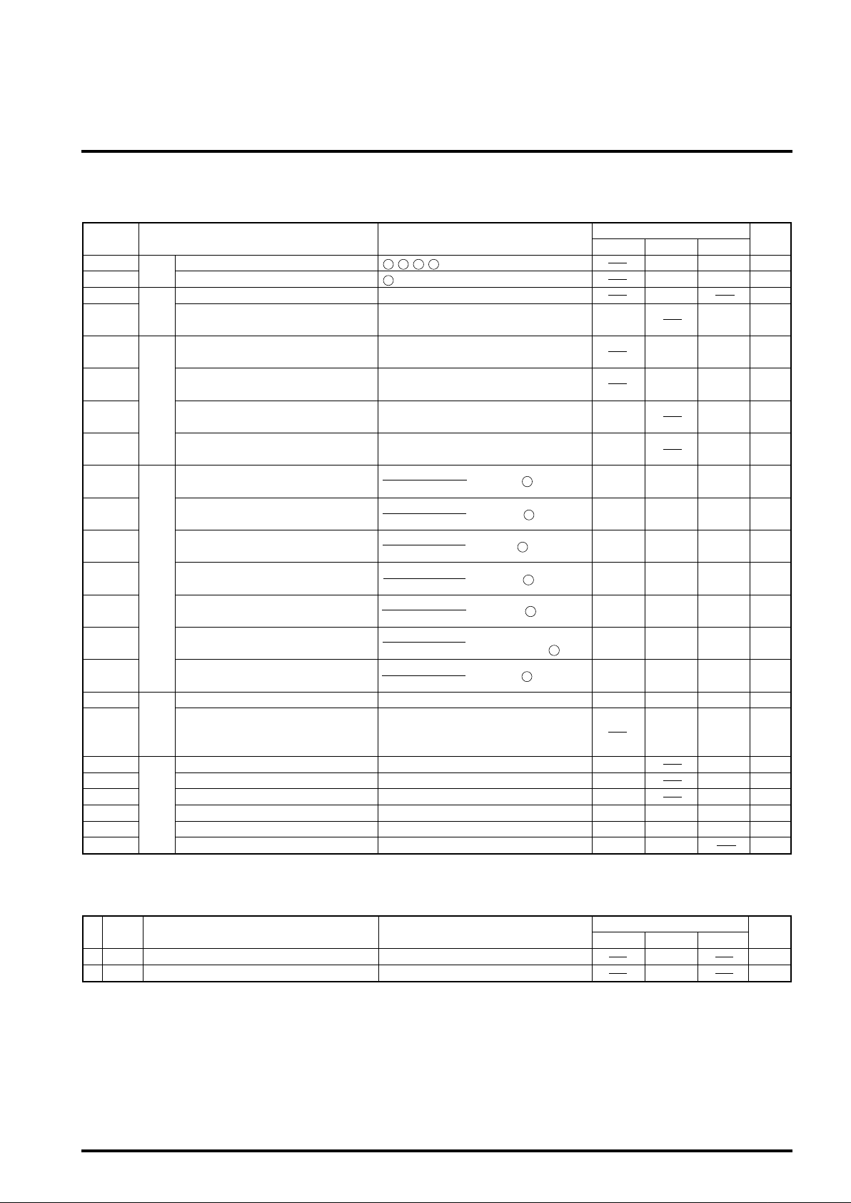
ELECTRICAL CHARACTERISTICS
(Ta=25˚C, VCC=Vbs1=Vbs2=Vm1=Vm2=5V, no-load unless otherwise noted)
Symbol Parameter Test conditions
ICC1 32 44 mA
I
CC2 10 14 mA
Vrefm
Vospm
Vsat1
Vsat2
Vofs1.2.3
Vofs4
Circuit current 1 on no-signal
Circuit current 2 on no-signal
circuit
Power
supply
Vrefm voltage
Spindle driver
driver
Output voltage D range
Spindle
Output saturation voltage
Output saturation voltage (At boot)
Output amp., Offset voltage
BTL driver
Output amp., Offset voltage
Gain1L Gain L between CH1 input and output
Gain1H Gain H between CH1 input and output
Gain2 Gain between CH2 input and output
Gain3L
Gain3H
Gain41
Gain42
Gain L between CH3 input and output
Gain H between CH3 input and output
Gain 1 between CH4 input and output
Gain between input and output
Gain 2 between CH4 input and output
2 , 3 , 29 , 30 pin current
1 pin current
IO=0.5A Vrefm reference
Top and bottom saturation voltage of
output power Tr (Io=0.5A)
Top and bottom saturation voltage of
output power Tr (Io=0.5A)
1,2,3ch amp., Vref=2.5V,
10kΩ connection between Vctl and Vref
4ch amp., Vref=2.5V
10kΩ connection between Vctl and Vref
{VM1(+)-VM1(-)}
(Vctl1L-Vref)
{VM1(+)-VM1(-)}
(Vctl1H-Vref)
{VM2(+)-VM2(-)}
(Vctl2-Vref)
{VM3(+)-VM3(-)}
(Vctl3L-Vref)
{VM3(+)-VM3(-)}
(Vctl3H-Vref)
{VM4(+)-VM4(-)}
{Vctl4(1)-Vref}
{VM4(+)-VM4(-)}
{Vctl4(2)-Vref}
(Vctl1L= pin)
(Vctl1H= pin)
(Vctl2= pin)
(Vctl3L= pin)
(Vctl3H= pin)
(10kΩ connection
with Vctl4(1)= pin)
(Vctl4L= pin)
4
5
13
19
20
28
31
Vrefin Vref amp. input voltage range
Min.
-1.55
-40
-70
6.2
18.8
31.8
5.1
10.2
22.6
36.5
Vrefs
Turn off the bias when the Vref input
Vrefs
Vopin
Vopout
Vofsop
Ibop
Ibofs
GB
Vref supervisory voltage
Vref amp.
Operational amp. input voltage range
Operational amp. output voltage range I
Operational amp. offset voltage
Operational amp. input current
OP amp.
Operational amp. input current offset
Operational amp. GB product
voltage is less than or equal to the value
at right.
O=±2mA
Vin=2.5V
Vin=2.5V
0.5
0.5
-10
-1
-100
2.3
Limits
Typ. Max.
2.15
1.55 V
1.35
0.7
1.9
1.0
+40
+70
6.7
19.3
32.3
5.6
10.7
25.0
37.0
2.5
1.4
7.2
19.8
32.8
6.1
11.2
27.2
37.5
V
CC-1.2
1.7
V
CC-1.0
V
CC-1.0
+10
-0.15
0
+100
4
0
MHz
Unit
V
V
V
mV
mV
dB
dB
dB
dB
dB
dB
dB
V
V
V
V
mV
µA
nA
CHECK ITEMS FOR EVALUATION
Symbol
Thermal Shutdown Operating Temperature
Ttsd
1
Thermal Shutdown Hysteresis Temperature
THtsd
2
The thermal shutdown temperature shown in this table does not assure the above thermal shutdown operating temperature range of the device operation. The
operating assurance range of the device covers up to Tjmax defined with the absolute maximum rating. The thermal shutdown operation shown in this table is a
thermal protection circuit applied when the temperature exceeds this Tjmax by mistake. Therefore, be sure to operate this device at the temperature lower than
or equal to Tj=150˚C.
Parameter
Test conditions
Min. Typ. Max.
Limits
165
40
Unit
˚C
˚C
 Loading...