Mitsubishi M56753FP Datasheet

MITSUBISHI <CONTROL / DRIVER IC>
)
M56753FP
2-CHANNEL ACTUATOR MOTOR DRIVER
DESCRIPTION
The M56753FP is a semiconductor IC developed as the motor
driver used DVD, DVD-ROM, CD-ROM and CD Player.
This device include 2 channel BTL drivers and can drive 2actuators
with one IC at the same time.
Also, the mute circuit, thermal protection circuit and VREF voltage
monitor circuit functions are included.
FEATURES
●Low output saturation voltage (typ. 1.35V at 0.5A).
● Wide operating supply voltage range (4.5 to 15V).
● High current drive capability (maximum 0.9A).
● Low crossover distortion.
● High frequency capability.
APPLICATION
DVD, DVD-ROM CD-ROM, CD PLAYER
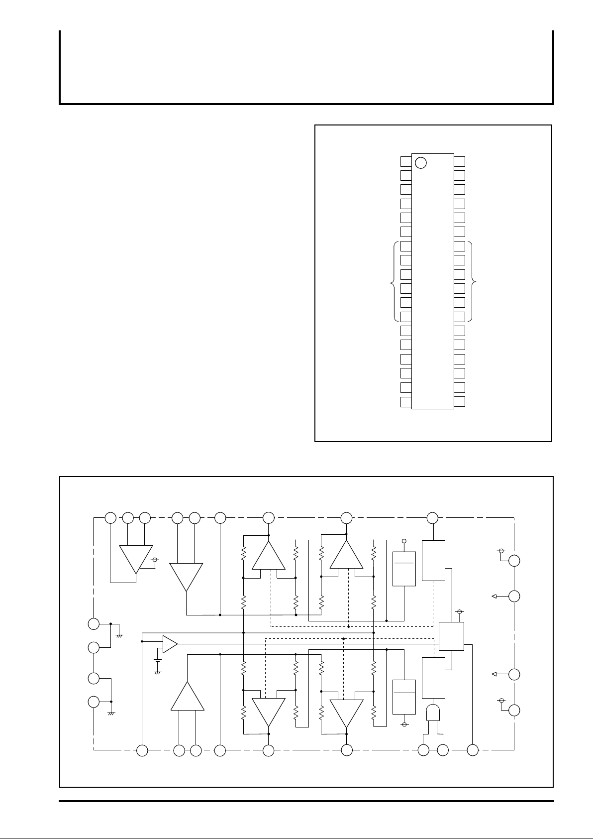
PIN CONFIGURATION(TOP VIEW
VBS1
VCC1
IN-
IN+
OPOUT
VM1+
GND
VM1-
CTL1OUT
CTL1+
CTL1-
TSDS
VREF
1
2
3
4
7
8
10
13
14
15 22
16
17
18
36
35
34
33
325
316
30
M56753FP
29
289
27
2611
2512
24
23
21
20
19
VBS2
VCC2
MUTE1
MUTE2A
MUTE2B
VM2+
GND
VM2CTL2OUT
CTL2+
CTL2N.C
N.C
BLOCK DIAGRAM
OPOUT
7
–
12
25
–
30
IN+ IN-
5 4 3
+
A3
GND
GND
VREF
CTL+
15 16
-
VBS2
-
+
A1
+
-
1.4V
A2
+
-
CTL2+ CTL2- CTL2OUT
CTL1OUT
14 6
25k 25k
5k 5k 5k 5k
5k 5k 5k 5k
25k 25k 25k 25k
23212218
VM1+
PA
x5
PA
31
VM2+
+-
x5
+
CH1
CH2
VM1-CTL1-
13 34
25k
PA
25k
+-
x5
x5
-
+
PA
24
VM2-
Outline 36P2R-D
MUTE1
VCC1
2
2
VCC 2
MUTE2A
CH1
MUTE
CH2
MUTE
VCC1
-0.35V
VCC 2
-0.35V
N.C : no connection
H
L or Open : Mute Off
TSD
H,H
Mute ON
MUTE2B
: Mute On
12v
VBS2
12v
173233
TSDS
VCC1
VBS1
12v
VBS2
12v
VCC2
2
1
36
35

MITSUBISHI <CONTROL / DRIVER IC>
)
M56753FP
2-CHANNEL ACTUATOR MOTOR DRIVER
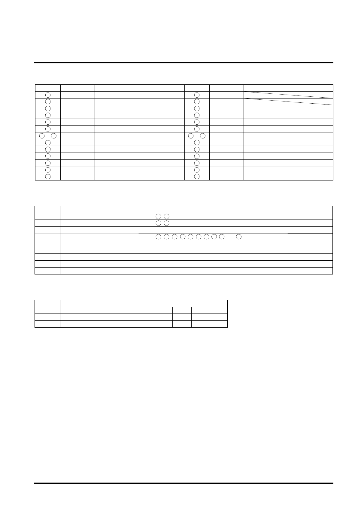
PIN DESCRIPTIONS
Symbol
1
2
3
4
5
6
7 12
to
13
14
15
16
17
18
VBS1
VCC1
ININ+
OPOUT
VM1+
GND
VM1CTL1OUT
CTL1+
CTL1TSDS
VREF
Bootstrap power supply 1
Power supply 1
Op-Amp. inverted input
Op-Amp. non-inverted input
Op-Amp. output
CH1 Amp. non-inverted output
GND
CH1 Amp. inverted output
CH1 input Amp. output
CH1 Amp. non-inverted input
CH1 Amp. inverted input
Thermal monitor
Reference voltage input
ABSOLUTE MAXIMUM RATINGS(Ta=25˚C
Symbol Ratings
VBS
VCC
IO
Vin
Pd
Kθ
Tj
Topr
Tstg
Bootstrap Power Supply
Power Supply
Output Current
Maximum Input Voltage of each Terminals
Power Dissipation
Thermal Derating
Junction Temperature
Operating Temperature
Storage Temperature
Parameter Conditions
1 36
, pins
2 35
, pins
V
CC=VBS=12V
3 4 15 16 18 21 22 32 33 34
, , , , , , , , and pins
With infinite heatsink
With infinite heatsink
Pin No. SymbolPin No. Function
19
20
21
22
23
24
25 30
to
31
32
33
34
35
36
N.C
N.C
CTL2CTL2+
CTL2OUT
VM2GND
VM2+
MUTE2B
MUTE2A
MUTE1
VCC2
VBS2
CH2 Amp. inverted input
CH2 Amp. non-inverted input
CH2 input Amp. output
CH2 Amp. inverted output
GND
CH2 Amp. non-inverted output
CH2 mute B
CH2 mute A
CH1 mute
Power supply 2
Bootstrap power supply 2
0 – Vcc
-20 – +75
-40 – +150
Function
15
15
900
4.5
27.8
150
Unit
V
V
mA
V
W
˚C/W
˚C
˚C
˚C
RECOMMENDED OPERATING CONDITIONS
Symbol
VCC1,2
VBS1,2
Power Supply
Bootstrap Power Supply
Limits
Min. Typ. Max.
12
VCC+1
UnitParameter
V
V
 Loading...