MITSUBISHI <CONTROL / DRIVER IC>
)
g
r
M56710FP
F2F MAGNETIC STRIPE ENCORDING CARD READER
DESCRIPTION
The M56710FP is a semiconductor integrated circuit of BiCMOS
structure having an F2F demodulator function for magnetic card
reader.
FEATURES
●Low current dissipation (0.7mA when on standby as a standard)
●Provided with glance-over selection input (4, 8, and 16 bits)
●Provided with output polarity (“L” active or “H” active) switching
input
●Miniature mini-mold package
●Wide operating temperature range Ta = -20 – 75°C
APPLICATION
Magnetic card reader
FUNCTION
Data signal which is read from magnetic card via magnetic head is
input from HD2 and HD1 pins, and converted into F2F pattern
signal by analog processing in amplifier OP1, differentiator OP2,
sensitivity setting circuit and waveform shaping circuit. If F2F signal
is input, the logic section glances over the prescribed number of
bits set by IB1 and IB2 input before performing digital processing,
and then outputs card reading signal CLS, read clock signal RCP,
and read data signal RDT. INV turning to “L” switches each output
of CLS, RCP and RDT from “L” active to “H” active.
• STANDARD BITS:
Let the number of glance-over bits set by IB1 and IB2 be M.
Let the Mth FC (flux change) through M+1st FC after LDI input is
turned from “L” to “H” be a standard bit with a time width of TB0.
I/O is discriminated from the next bit to this standard bit as a data
bit.
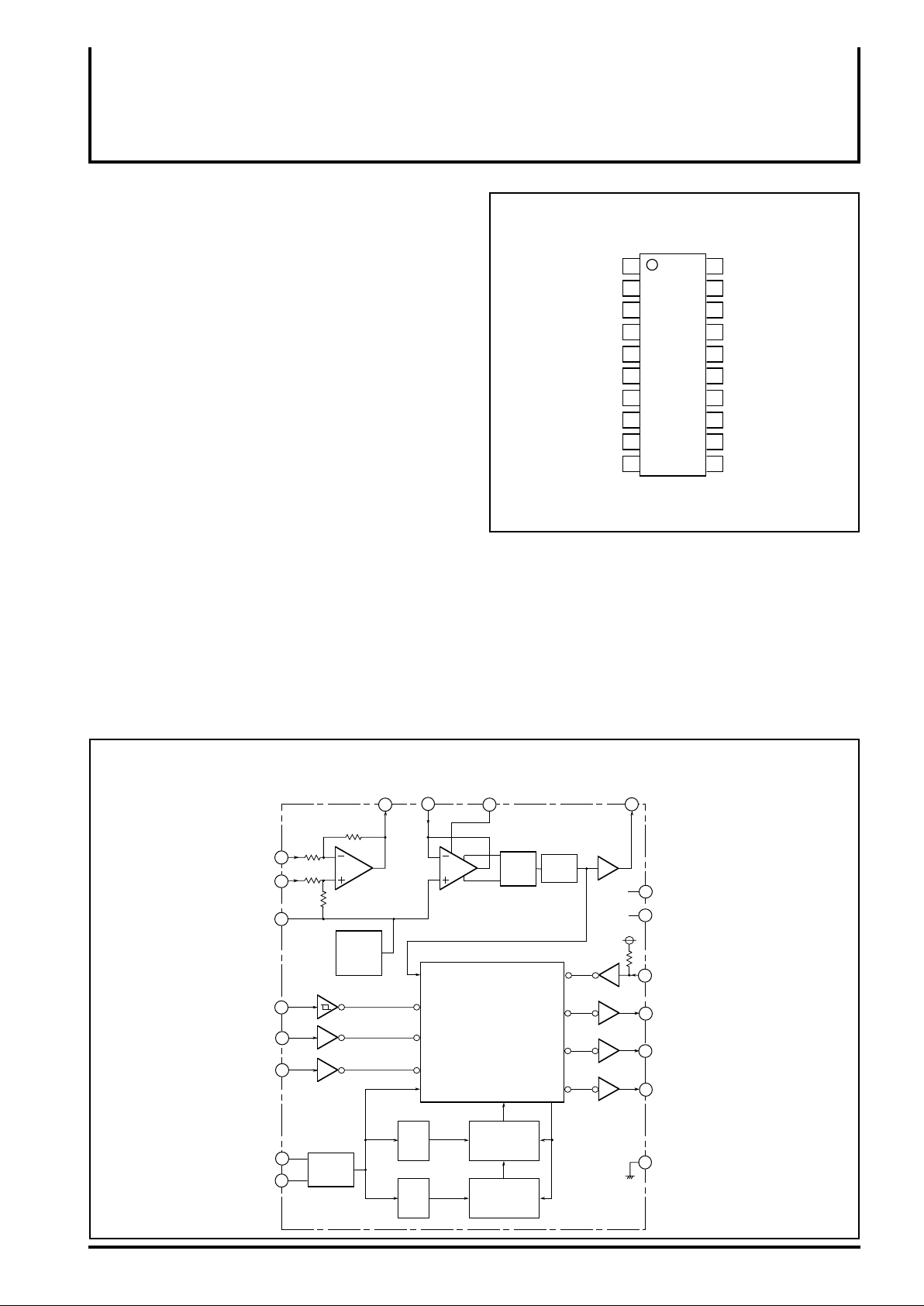
PIN CONFIGURATION(TOP VIEW
→
Read control input
F2F output
Noise filter
Differentiator input
Amplifier output
Amplifier (–) input
Amplifier (+) input
Standard voltage
output
Grounding
LDI
NC
F2F
PKO
PKI
AMP
HD2
HD1
VRF
GND
1
2
←
3
4
→
←
→
→
9
20
19
18
M56710FP
17
165
156
147
138
12
1110
Outline 20P2N-A
• I/O discrimination
Let the data bit time width of a data bit be TBn, and if there is one
next FC between the FC at the end of that bit (i.e. the beginning
of the next bit) to 5/7TBn, let the next bit (Bn+1) be data “1”, and,
if there is no FC, be data “0”.
• Output signal time width
When letting the oscillation cycle of oscillation circuit be TOSC,
• RCP output pulse width TOW•••••••••••••••••••••••about 16TOSC
• RCP delay time to RDT•••••••••••••••••••••••••••••••about 8TOSC
VCC1
VCC2
CX1
CX2
←
IB1
←
IB2
←
INV
→
CLS
→
RDT
→
RCP
Power supply
Power supply
Oscillation capacitor
Oscillation capacitor
Ignore bit 1
Ignore bit 2
Invert input
Card travelling
signal output
Read data output
Read clock output
NC: no connection
BLOCK DIAGRAM
Amplifier (-) input
Amplifier (+) input
e output
Read control input
Ignore bit 2
HD2
HD1
VRFReference volta
LDI
IB2
IB1Ignore bit 1
CX2Oscillation capacito
CX1Oscillation capacitor
Amplifier
output
7
8
9
Reference
voltage
circuit
1
15
16
17
Oscillation
circuit
18
AMP
OP1
T
OSC
Differentiator
input
6
1/5
1/7
PKI
5
OP2
Control circuit
5T
OSC
7TOSC
Noise filter
PKO
4
Sensitivity
setting
11 bit
downcounter
11 bit
upcounter
Waveform
shaping
F2F output
F2F
3
20
19
14
13
12
11
10
Power supply
VCC1
V
CC2
Power supply
INV
Invert input
CLS
Card travelling signal output
RDT
Read data output
RCP
Read clock output
GND

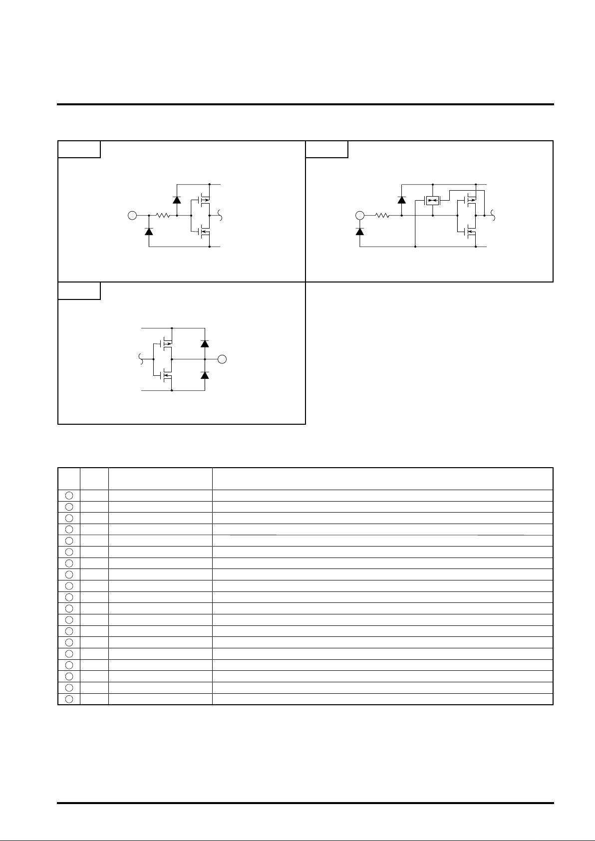
I/O CIRCUIT
MITSUBISHI <CONTROL / DRIVER IC>
M56710FP
F2F MAGNETIC STRIPE ENCORDING CARD READER
1 2
3
LDI, IB1, IB2 input circuit INV input circuit
CC2
V
LDI
IB1
IB2
GND
CLS, RDT, RCP output circuit
VCC2
CLS
RDT
RCP
GND
INV
V
CC2
GND
PIN FUNCTION DESCRIPTION
Pin
No.
10
11
12
13
14
15
16
17
18
19
20
Pin
name
1
LDI
Read control input
3
F2F
F2F output
4
PKO
Noise filter
5
PKI
Differentiator input
6
AMP
Amplifier output
7
HD2
Amplifier (–) input
8
HD1
Amplifier (+) input
9
VRF
Reference voltage output
GND
Grounding
RCP
Read clock output
RDT
Read data output
CLS
Card travelling signal output
INV
Invert input
IB2
Ignore bit 2
IB1
Ignore bit 1
CX2
Oscillation capacitor
CX1
Oscillation capacitor
V
Power supply
CC2
Power supply
VCC1
Name Function
Schmidt trigger input. At “L”, reset the internal digital circuit. At “H”, F2F modulation is possible.
F2F signal output that has amplified, differentiated and further waveform-shaped the magnetic head signal.
Connect noise removing capacitor CNF between PKI and PKO.
Refer to PKO and AMP.
Connect resistor RPK and capacitor CPK between AMP and PKI.
Connect magnetic head between HD1 and HD2.
Connect magnetic head between HD1 and HD2.
Reference voltage output of Vcc 1/2
Clock pulse output after F2F modulation
Data output after F2F modulation
Signal output indicating that card is travelling
CLS, RDT and RCP output becomes “L” active at “H” (OPEN), and “H” active at “L”.
Glance-over bit setting pin
Glance-over bit setting pin
Connect capacitor C
Connect capacitor C
OSC between CX1 and CX2 to set oscillation frequency.
OSC between CX1 and CX2 to set oscillation frequency.
Digital circuit section power supply pin. Supply voltage is Vcc.
Analog circuit section power supply pin. Supply voltage is Vcc (same voltage as Vcc
2).

F2F MAGNETIC STRIPE ENCORDING CARD READER
”
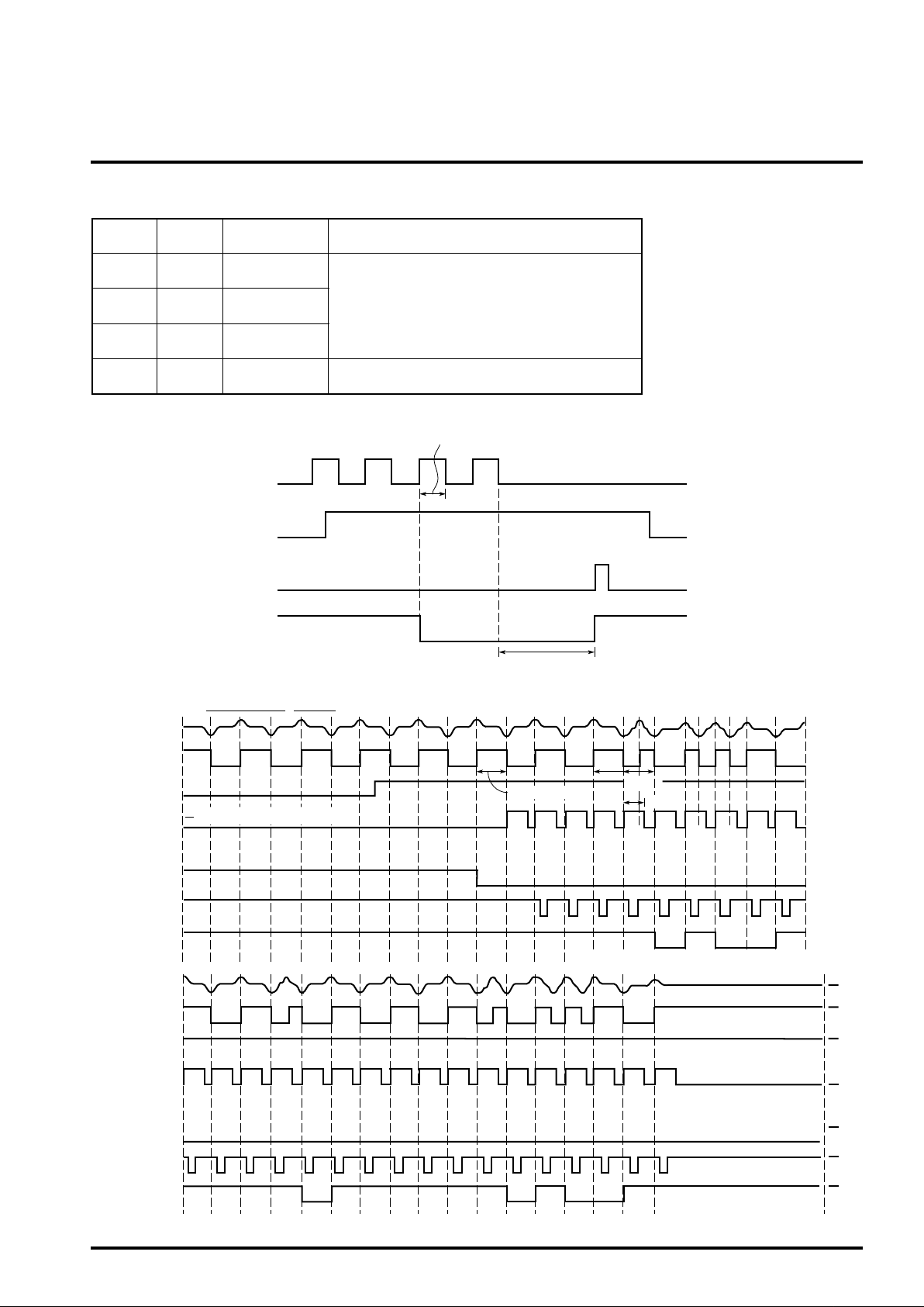
GLANCE-OVER BIT SETTING AND TIMING BY IB1 AND IB2
IB2 input IB1 input
LL
LH
HL
Number of
glance-over bits
4
8
16
Description
• Internal digital circuit is reset with LDI input at “L”.
• LDI input may be at “H” at all times.
• CLS output turns to “L” after counting the flux change
FC (change in the status of F2F) of the number of
glance-over bits, and returns to “H” when BIC (bit
interval counter) has fully counted. (At “L” active).
MITSUBISHI <CONTROL / DRIVER IC>
M56710FP
HH
——
• IB2, IB1: “L”, “L”
x1234
F2F
LDI
BIC
full count
CLS
OPERATING TIMING DIAGRAM
INV : “H”
HD2 - HD1
F2F
LDI
(5/7)
IB2, IB1 : “L”, “L
Bit 1/0 discrimination signal
TBO : Reference bit
About 14300 T
TB0 TBn
Reference bit
OSC
TBn+
5/7TBn
CLS
RCP
RDT
HD2 - HD1
F2F
LDI
(5/7)
CLS
RCP
000 0 100000010110 0
RDT
0000 10110
RDT data is output 1 bit behind F2F data.
 Loading...