


MITSUBISHI <CONTROL / DRIVER IC>
K
M56692FP
Bi-CMOS & DMOS 32BIT SERIAL-INPUT LATCHED DRIVER
DESCRIPTION
The M56692FP is a semiconductor integrated circuit that has a
built-in, 32-bit shift register and a latch of CMOS structure with
serial input and serial/parallel output, and a 32-bit totem-pole-type
parallel output driver of high pressure proof DMOS structure.
Employed are Bi-CMOS and high pressure proof DMOS
processing technology.
FEATURES
● Serial input - serial/parallel output
● Bidirectional shift register (controlled at F/R terminal)
● Cascade connections possible through serial output.
● Latch circuit included for each stage.
● Driver supply voltage: VH=90V
● Operating temperature: -40 – 85°C
APPLICATION
Vacuum Fluorescent Display GRID DRIVER
PIN CONFIGURATION (TOP VIEW)
HVO22
HVO21
HVO20
HVO19
HVO18
HVO17
HVO16
HVO15
HVO14
HVO23
HVO24
HVO25
HVO26
HVO27
HVO28
HVO29
HVO30
HVO31
HVO
PGND
3332313029282726252423
34
35
36
37
38
39
40
41
42
32
43
44
M56692FP
123456789
VH
F/R
VDD
SOUT(SIN)
CLK
LGND
LAT
BLK
SIN(SOUT)
Outline 44P6N-A
HVO13
10
H
V
HVO12
22
21
20
19
18
17
16
15
14
13
12
11
PGND
HVO11
HVO10
HVO 9
HVO 8
HVO 7
HVO 6
HVO 5
HVO 4
HVO 3
HVO 2
HVO 1
BLOCK DIAGRAM
Output
protect
circuit
VDD
3
BL
8
LAT
SIN
5
7
9
6
LGND
(SOUT)
CLK
L D
HVO32HVO31HVO30HVO 3HVO 2HVO 1
42 4341141312
1
H
V
10
11
PGND
44
Q
QTD
L D
Q
QTD
L D
Q
QTD
L D
Q
QTD
L D
Q
Q
L D
QTD
QTD
2
4
SOUT
(SIN)
F/R
3-58
MITSUBISHI <CONTROL / DRIVER IC>
PIN FUNCTION DESCRIPTION
↓
↓
M56692FP
Bi-CMOS & DMOS 32BIT SERIAL-INPUT LATCHED DRIVER
FUNCTION
The M56692FP comprises a 32 bit bidirectional shift register, a 32
bit latch, and a parallel output HVO 1 – HVO32 connected to its
output.
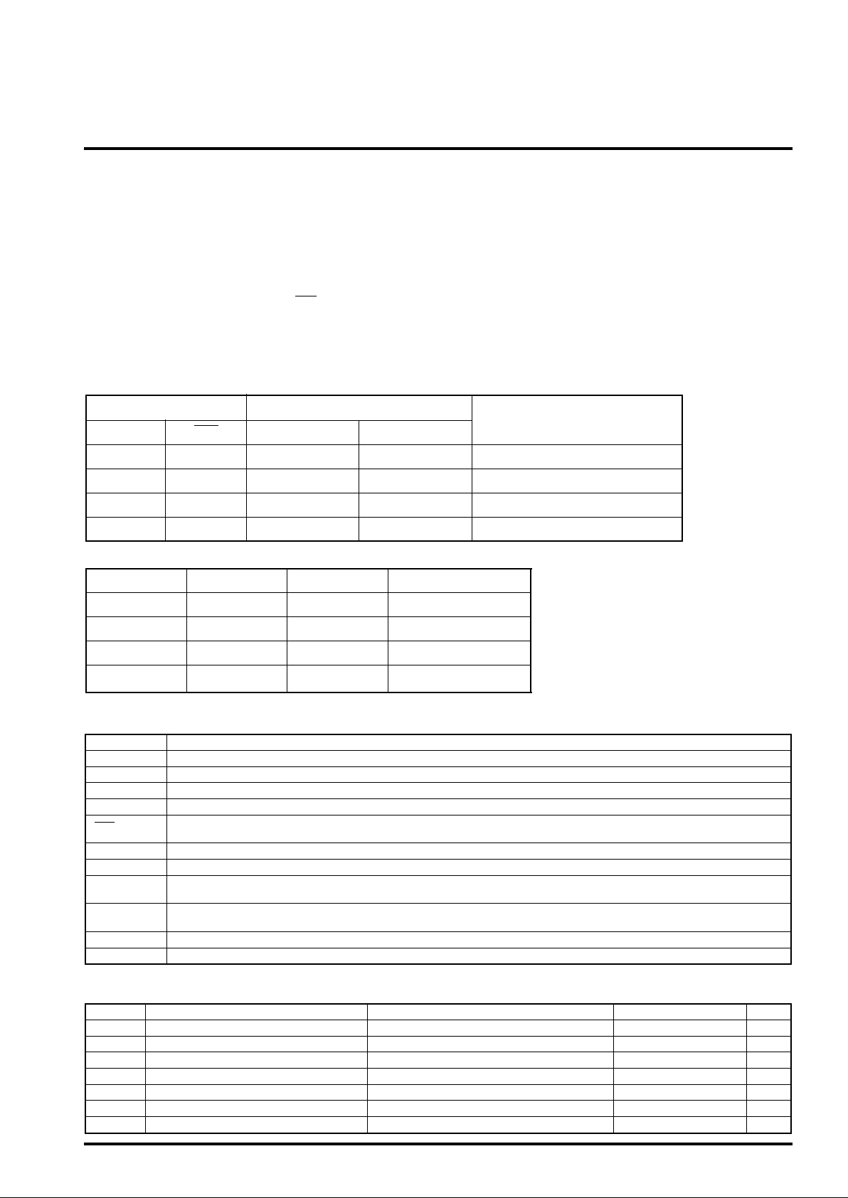
In accordance with truth table 1, the data transfer direction of shift
register depends upon F/R input, and F/R being at “H” or open
allows pin 9 to turn to SIN and pin 2 to turn to SOUT, and F/R
being at “L” allows pin 2 to turn to SIN and pin 9 to turn to SOUT,
permitting data transfer from SIN to SOUT, respectively.
Inputting data to SIN and clock pulse to CLK allows SIN signal to
be put into the internal shift register when the clock changes from
“H” to “L”, and shift register data to be shifted sequentially.
TRUTH TABLE
Truth table 1. Shift register section
Input Input/output
F/R
H
H
L
L
CLK
H or L
H or L
SIN(SOUT)
IN
IN
OUT
OUT
SOUT(SIN)
OUT
OUT
IN
IN
Truth table 2. Latch and driver sections
X
H
L
X
H
H
H
L
L
Serial-output SOUT is used by connecting to the next stage
M56692FP SIN when more than one M56692FP is used to expand
bits in the series.
In accordance with truth table 2, parallel output allows the latch to
pass data through if LAT input is turned to “H”, and data to be
retained if LAT input is turned to “L”. Driver output HVOn allows
data from the latch to be output if BLK input is turned to “L”, and “L”
to be output if BLK input is turned to “H” irrespective of data from
the latch.
Shift register
DATA is shifted.
No changes.
DATA is shifted.
No changes.
HVOnDn LAT BLK
Output all “L”
H
L
Dn=nth bit DFF retention data
HVOn=nth bit driver output
L = “L” level
H = “H” level
X = “L” level or “H” level
X
Pin name
VDD
LGND
V
H
PGND
CLK
SIN
SOUT
LAT
BLK
F/R
HVO1–32
Logic stage supply voltage
Logic stage ground
Output stage supply voltage
Output stage supply ground
Clock input for the internal shift resister. The data enter the internal shift resisters and the data in the shift registers will be
shifted in order by High to Low change of the clock.
Serial data input
Serial data output
Latch input. When the LATCH is set to “H”, the data in the shift resister will enter the each latch circuit.
When the LATCH input is set to “L”, the data will be held.
Enable input for output control. When the BLK input is set to “L”, data in the latch circuit will appear at outputs.
When the BLK input is set to “H”, all outputs will be set to “L”.
Direction Control for the internal shift resister
Output driver (push-pull)
L
L
Latch’s data output.
Function
ABSOLUTE MAXIMUM RATINGS (Ta=25°C, unless otherwise noted)
Symbol
VDD
H
V
VI
O
V
V
HVO
Pd
Tstg
Logic stage supply voltage
Output stage supply voltage
Logic inputs voltage
Logic output voltage
Output voltage
Power dissipation range
Storage temperature range
Data output
High supply voltage output pin
Ta ≤ 25°C
Conditions
Ratings UnitParameter
-0.3 – 7
-0.3 – 90
-0.3 – V
DD+0.3
-0.3 – VDD+0.3
H
-0.3 – V
850
-55 – 150
V
V
V
V
V
mW
°C
 Loading...