

Mitsubishi M56620AP Datasheet
MITSUBISHI <CONTROL / DRIVER IC>
)
M56620AP
Bi-CMOS 8-BIT PARALLEL-INPUT LATCHED DRIVER
DESCRIPTION
The M56620AP is a semiconductor integrated circuit fabricated
using Bi-CMOS technology. It contains bipolar 8 output drivers of
CMOS latch.
FEATURES
● Enable input for output control
● Low supply current .......................................ICC≤10µA at standby
● Input level is compatible with standard CMOS
● Driver: Withstand voltage ...........................................BVCEO≥50V
Large drive current .................................. (IO(max)=500mA)
● Wide operating temperature range ..................... Ta=-20 – +75°C
APPLICATION
Thermal printer head dot driver, Relay driver, Solenoid driver
FUNCTION
When data is applied to inputs IN1 – IN8 and LATCH input is set to
“H”, the data will be latchedance with the truth table. Note that
when an “H” signal is applied to the RESET input, the latch will
maintain the reset state.
When the EN input is set to “L” and the data maintained in the latch
are “H”, the corresponding output will be ON and become “L”.
When both the LATCH and RESET inputs are “L”, the latch will
maintain the prior state irrespective of input signals IN1 – IN8.
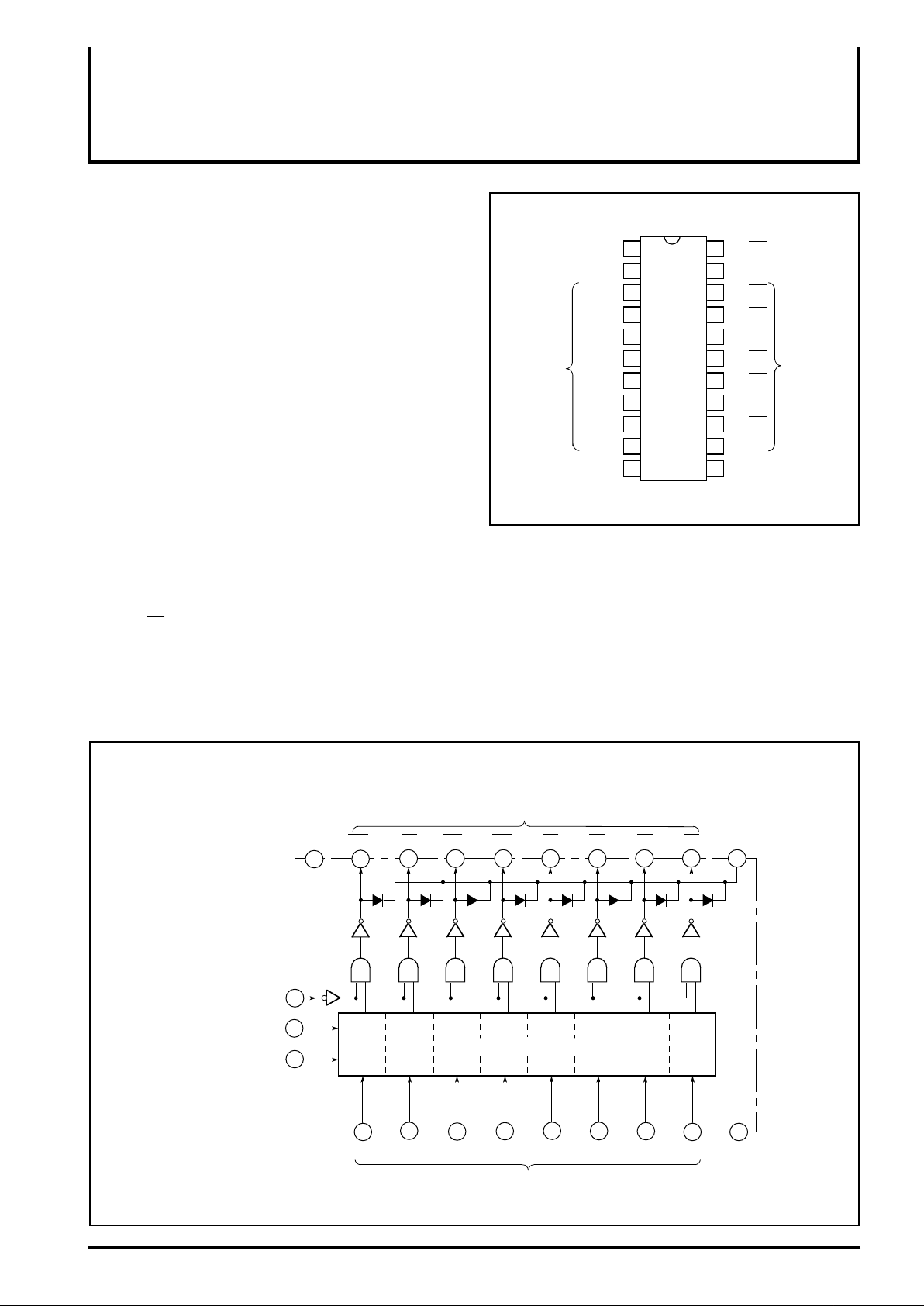
PIN CONFIGURATION(TOP VIEW
→
Reset input
Latch input
Parallel inputs
RESET
LATCH
IN1
IN2
IN3
IN4
IN5
IN6
IN7
IN8
GND
1
→
2
→
3
→
4
→
→
→
→
→
→
Outline 22P4
22
21
20
19
M56620AP
185
176
167
158
149
1310
1211
←
→
→
→
→
→
→
→
→
Enable input
EN
CC
V
O1
O2
O3
O4
Parallel outputs
O5
O6
O7
O8
COM
COMMON
BLOCK DIAGRAM
Enable input
Reset input
Latch input
EN
RESET
LATCH
Parallel outputs
O1 O2 O3 O4 O5 O6
2021
22
1
2
IN1 IN2 IN3 IN4 IN5 IN6 IN7 IN8 GND
19 18 17 16 15
(8 latch circuits)
4
3
5
6
Parallel inputs
7
O7 COMO8VCC
14 13 12
8 9
COMMON
10 11
TRUTH TABLE
Input
INn
L
H
x
x
x
LATCH
H
H
x
x
L
RESET
L
L
H
x
L
EN
L
L
x
H
L
xLLLHH
Output On
t-1
x
x
x
x
L
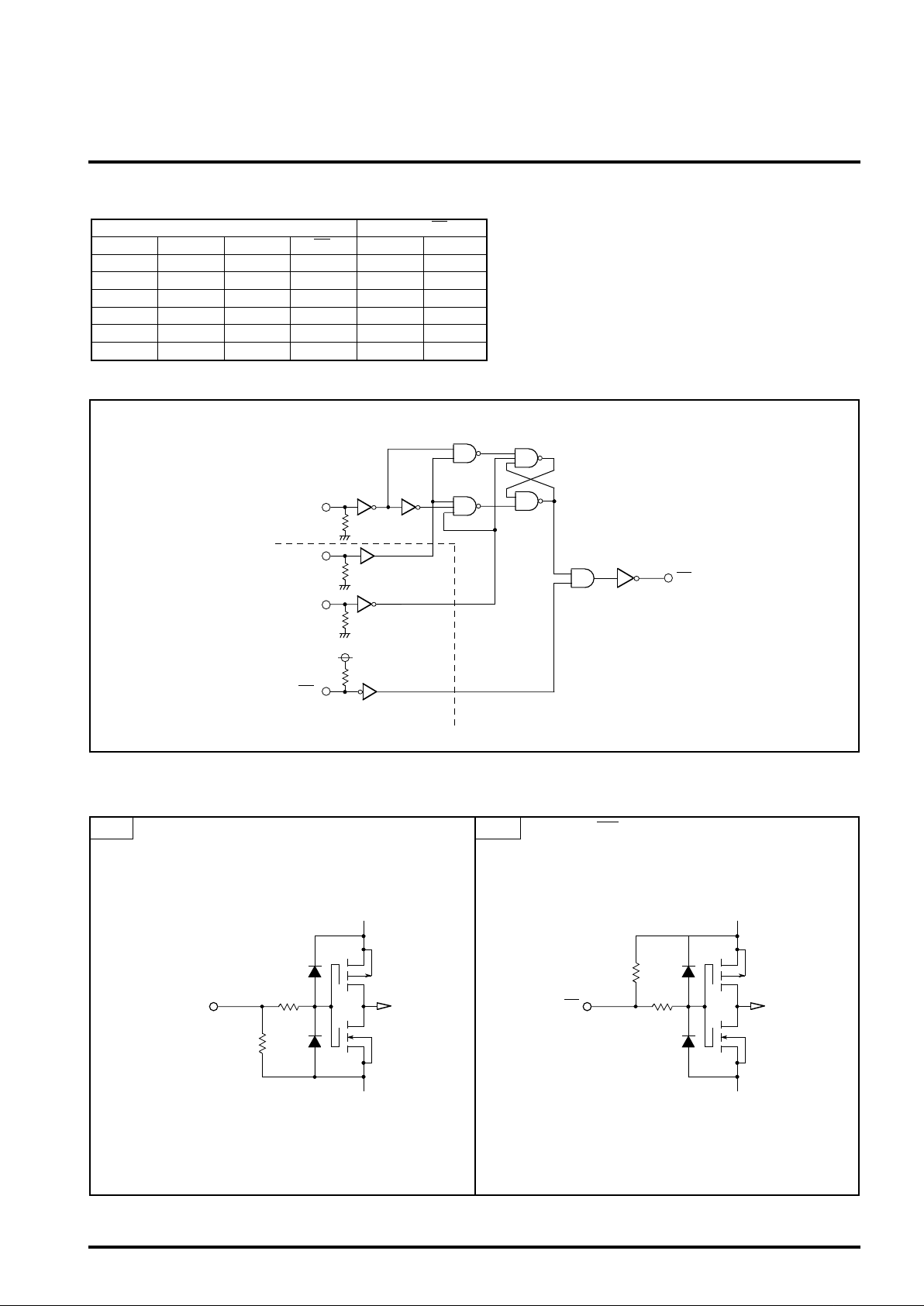
LOGIC DIAGRAM (One circuit)
INn
MITSUBISHI <CONTROL / DRIVER IC>
M56620AP
Bi-CMOS 8-BIT PARALLEL-INPUT LATCHED DRIVER
t
H
L
H
H
L
L: low level
H: high level
x: low level or high level
t-1: previous state
t: current state
H output: OFF state
L output: ON state
LATCH
RESET
CC
V
EN
Common block
INPUT/OUTPUT EQUIVALENT CIRCUITS
1 Input circuits
(INn, LATCH, RESET)
VCC
INn
(n = 1 – 8)
RIN
(n = 1 – 8)
2 Input circuit (EN)
R
IN
EN
On
VCC
GND
GND
 Loading...