

MITSUBISHI <CONTROL / DRIVER IC>
)
M54974P
Bi-CMOS 12-BIT SERIAL-INPUT LATCHED DRIVER
DESCRIPTION
The M54974P is a semiconductor integrated circuit consisting of 12
stages of CMOS shift registers and latches with serial inputs and
serial or parallel outputs. It is based on Bi-CMOS process
technology, and has 12 bipolar drivers at the parallel outputs.
FEATURES
● Serial input and serial or parallel output
● Serial output enables cascade connection
● Built-in latch for each stage
● Enable input provides output control
● Low supply current (standby current ICC≤10µA)
● Serial I/O level is compatible with typical CMOS devices
● Driver features: High withstand voltage (BVCEO≥30V)
Capable of large drive currents (IO(max)=300mA)
● Wide operating temperature range Ta=-20 – +75°C
APPLICATION
Dot drivers for thermal print heads. Serial/parallel conversion.
Drivers for relay and solenoids.
FUNCTION
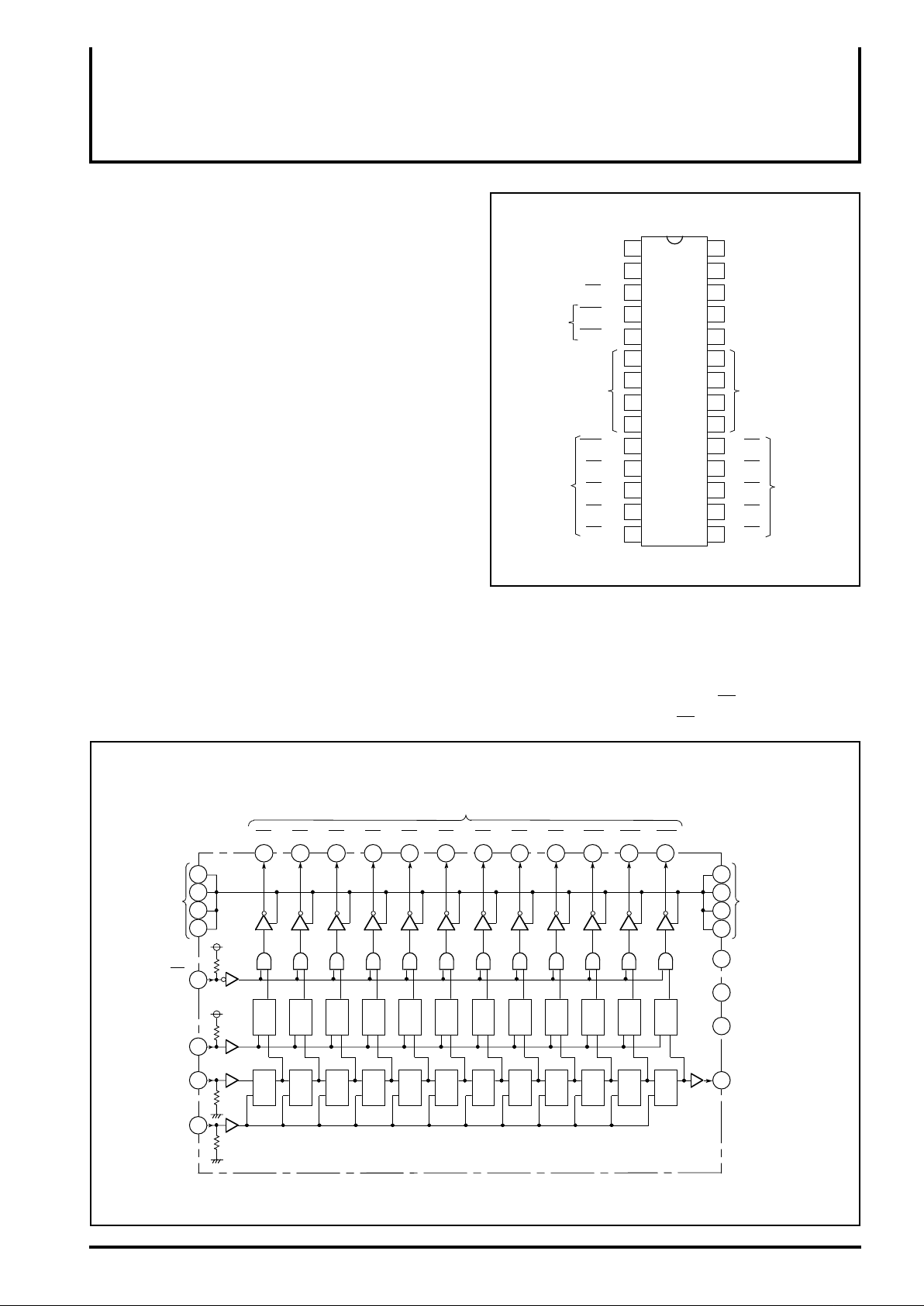
The M54974P consists of 12 stages of D-type flip flops connected
to 12 latches.
Data is input to serial input S-IN, and clock pulses are applied to
clock input T. When the clock changes from low to high, the input
data enters the first shift register and data already in the shift
PIN CONFIGURATION(TOP VIEW
Serial output
Latch input
Enable input
Parallel outputs
Driver GND
Parallel outputs
S-OUT
LATCH
EN
O12
O11
P-GND
O10
O9
O8
O7
O6
←
1
→
2
→
3
←
4
←
7
8
←
←
←
12
←
13
←
14
M54974P
28
27
←
26
←
25
245
236
22
21
209
→
1910
→
1811
→
17
→
16
→ O5
15
Outline 28P4B
registers is shifted sequentially.
The serial output S-OUT is used to connect multiple M54974Ps to
expand the number of parallel outputs. S-OUT is connected to S-IN
of the next stage.
When the clock pulse changes from low to high, latch input
(LATCH) is high and output enable input (EN) is low the serial input
data at S-IN appears at output O1 and the other data already
CC
L-V
L-GND
S-IN
T
CC
P-V
P-GND
O1
O2
O3
O4
Logic power
supply
Logic GND
Serial input
Clock
Output power
supply
Driver GND
Parallel outputs
BLOCK DIAGRAM
6
EN
LATCH
S-IN
Clock
7
8
9
L-VCC
3
L-V
2
26
T
25
P-GND
Driver GND
Enable input
Latch input
Serial input
Parallel outputs
O1
O2
O3
O4
O5
O6
O7
O8
O9
O10
O11
O12
19
18 17 16 15 14 13 12 11 10 5 4
20
21
P-GND
Driver GND
22
23
P-VCC
24
Output power supply
CC
L-V
23
CC
Q
Q
Q
Q
Q
Q
Q
Q
Q
Q
Q
Q
L D
L D
L D
L D
L D
L D
L D
L D
L D
L D
L D
L D
QTD
QTD
QTD
QTD
QTD
QTD
QTD
QTD
QTD
QTD
QTD
QTD
Logic power supply
L-GND
27
Logic GND
S-OUT
1
Serial output
MITSUBISHI <CONTROL / DRIVER IC>
M54974P
Bi-CMOS 12-BIT SERIAL-INPUT LATCHED DRIVER
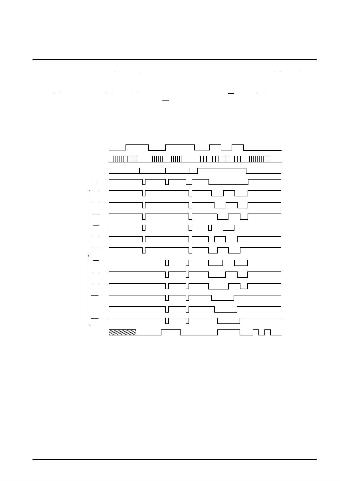
present is shifted sequentially to outputs O2 through O12.
The parallel outputs are inverted.
When the latch input is held low, the latch retains the stored data.
When the EN input is high, outputs O1 through O12 all turn off. As
the internal logic is unstable when the power is turned on, the EN
TIMING CHART
Serial input
S-IN
TClock
LATCHLatch input
ENEnable input
O1
O2
O3
O4
O5
input should be kept high (setting the outputs O1 through O12 off)
until input data is set and the internal logic is initialized.
L-GND is the GND of CMOS logic circuit and P-GND is the GND of
output driver circuits O1 through O12 which employ bipolar
transistors capable of large drive currents.
Parallel outputs
O6
O7
O8
O9
O10
O11
O12
S-OUTSerial output
* The shaded area shows the unstable state.
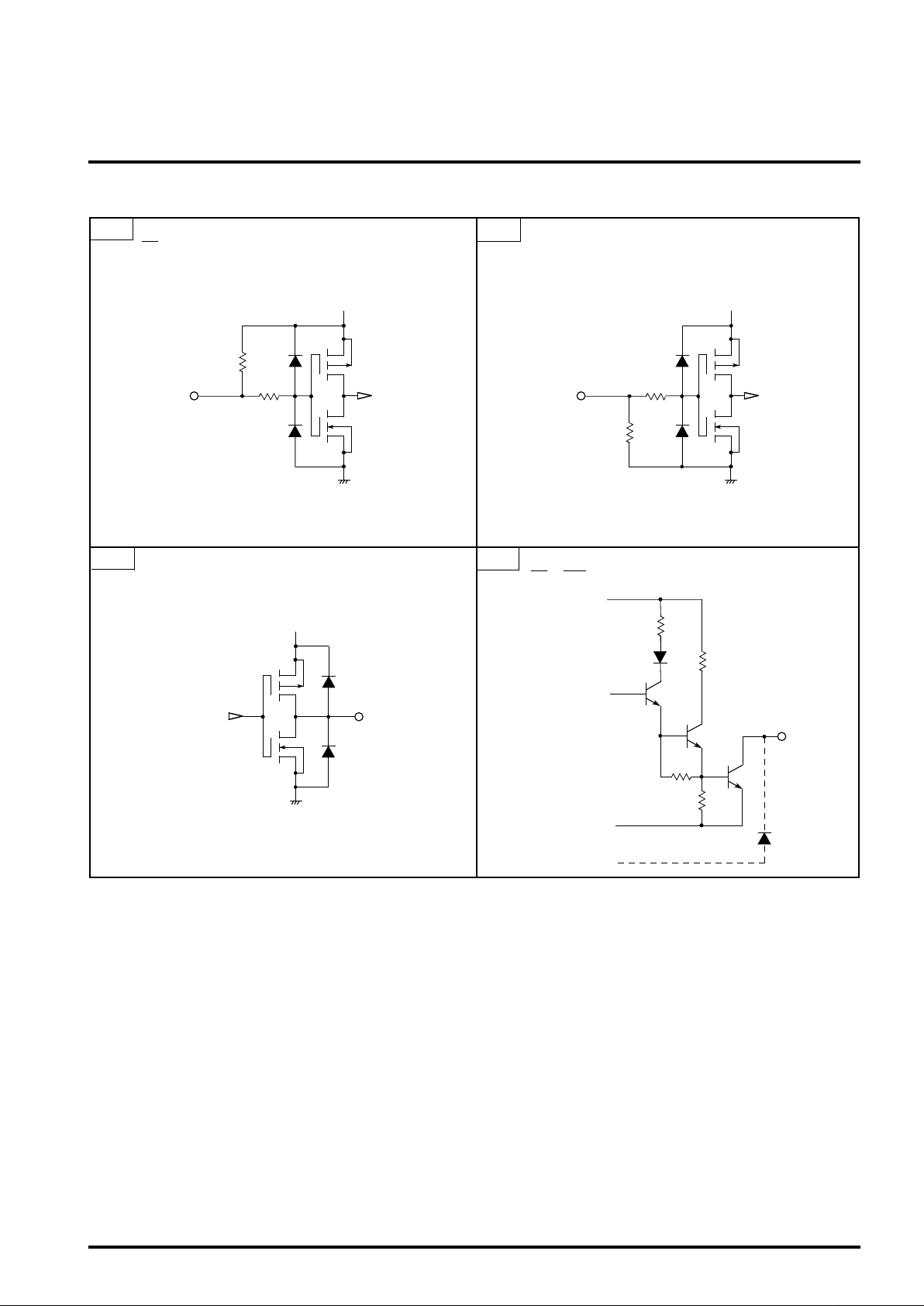
INPUT/OUTPUT CIRCUIT DIAGRAM
1 Inputs with pullup resistor
(EN, LATCH)
MITSUBISHI <CONTROL / DRIVER IC>
M54974P
Bi-CMOS 12-BIT SERIAL-INPUT LATCHED DRIVER
2 Inputs with pulldown resistor
(T, S-IN)
3 Serial output
(S-OUT)
RIN
L-VCC
L-VCC
L-GND
4 Parallel outputs
(O1 – O12)
P-V
CC
L-VCC
RIN
L-GND
L-GND
P-GND
L-GND

MITSUBISHI <CONTROL / DRIVER IC>
Bi-CMOS 12-BIT SERIAL-INPUT LATCHED DRIVER
ABSOLUTE MAXIMUM RATINGS (Ta=-20 to 75°C, unless otherwise noted)
Symbol Ratings UnitParameter Conditions
M54974P
VCC
VI
VO
IO
Pd
Topr
Tstg
Supply voltage
Input voltage
Output voltage
Output current
Power dissipation
Operating temperature
Storage temperature
CC, L-VCC
P-V
S-IN, LATCH, T, EN
S-OUT
O1 – O12 : OFF
O1 – O12
T
a=25°C
-0.5 – 8
-0.5 – V
-0.5 – V
-0.5 – 30
400
2.5
-20 – 75
-55 – 125
RECOMMENDED OPERATING CONDITION (Ta=-20 to 75°C, unless otherwise noted)
Symbol
VCC
VO
IO
Supply voltage
Output apply voltage
Output current (per circuit)
Conditions UnitParameter
P-VCC, L-VCC
O1 – O12 : OFF
All outputs go in the ON state simultaneously.
Duty cycle < 50%, Ta < 25°C
Limits
Min. Typ. Max.
456
ELECTRICAL CHARACTERISTICS (Ta=25°C, L-VCC=5V, P-VCC=5V, unless otherwise noted)
Symbol
VIH
VIL
RIN
VOH
VOL
IOH
IOL
VOL1
VOL2
VOL3
IOLK
ICC1
ICC2
ICC3
Parameter
High-level input voltage
Low-level input voltage
Input resistance
High-level output voltage
Low-level output voltage
High-level output current
Low-level output current
Low-level output voltage
Output leak current
Supply current (L-V
CC)
Output supply current (P-VCC)
S-OUT
S-OUT
S-OUT
S-OUT
O1 – O12
O1 – O12
Test conditions
T
a=-20 – 75°C
|IO|≤1µA
VOH=4.5V
VOL=0.4V
I
OL=120mA
OL=400mA
I
V
O=30V
Input: open, All driver outputs: OFF
One driver output is ON.
One driver output is ON.
0.7V
Limits
Min. Typ. Max.
CC
0
50
4.9
-100
400
CC+0.5
CC+0.5
30
300
V
CC
0.3VCC
0.1
0.4
0.7
50
10
0.2
14
V
V
V
mA
W
°C
°C
V
V
mA
Unit
V
V
kΩ
V
V
µA
µA
V
V
µA
µA
mA
mA
Bi-CMOS 12-BIT SERIAL-INPUT LATCHED DRIVER
TIMING REQUIREMENTS (Ta=-20 to 75°C, unless otherwise noted)
Symbol
f(T)
tw(T)
tw(L)
tsu
th
td(T-L)
tr(T)
tf(T)
Clock frequency
Clock pulse width
Latch pulse width
Data setup time
Data hold time
Clock-latch time
Clock pulse rise time
Clock pulse fall time
Input duty: 40 – 60%
Test conditions UnitParameter
TIMING CHART
MITSUBISHI <CONTROL / DRIVER IC>
M54974P
Limits
Min. Typ. Max.
2 MHz
200
200
100
100
400
500
500
ns
ns
ns
ns
ns
ns
ns
Serial input
Clock
Latch input
S-IN
LATCH
2.5V
tsu
T
h
t
2.5V 2.5V
tw(T) tr(T)
td(T-L)
2.5V
10%
2.5V 2.5V
tw(L)
SWITCHING CHARACTERISTICS (Ta=25°C, VCC=5V, unless otherwise noted)
Symbol
tPLH
tPHL
tPLH
tPHL
tPLH
tPHL
Low-to-high-level output propagation time, From input T to output S-OUT
High-to-low-level output propagation time, From input T to output S-OUT
Low-to-high-level output propagation time, From input T to output O
High-to-low-level output propagation time, From input T to output ON
Low-to-high-level output propagation time, From input EN to output ON
High-to-low-level output propagation time, From input EN to output ON
Test conditions UnitParameter
VIH=5V
VIL=0V
N
RL(S-OUT)=∞
RL(ON)=100Ω
(N=1–12)
CL=15pF
90%
90%
tr(T)
Limits
Min. Typ. Max.
(0.15)
(0.15)
(2)
(1)
(2)
(1)
10%
0.3
0.3
10
5
10
5
µs
µs
µs
µs
µs
µs
TIMING CHART
Clock
Serial output
Enable input
Output
S-OUT
EN
ON
T
2.5V
tPLH
2.5V
tPHL
2.5V
t
PLH
2.5V
2.5V
2.5V
2.5V
tPLHtPHL
2.5V
2.5V
tPHL
2.5V

TEST CIRCUIT
MITSUBISHI <CONTROL / DRIVER IC>
M54974P
Bi-CMOS 12-BIT SERIAL-INPUT LATCHED DRIVER
Input
PG
50Ω
The input waveform: tr ≤ 20ns, tf ≤ 20ns
The capacitance C
L includes the stray wiring
capacitance and probe input capacitance.
TYPICAL CHARACTERISTICS
Thermal derating
(Absolute maximum rating)
3.0
2.0
VCC
M54974P
RL
Output
CL
Duty cycle vs. allowable
output current
400
300
–
176
8
9
10
11
12
1.0
Power dissipation Pd (W)
0
0
25 50 75 100
Ambient temperature Ta (°C)
Duty cycle vs. allowable
output current
400
300
200
Collector current : current per circuit
Repetitive frequency ≥ 10H
The figure in a circle shows the number
100
Output current Io (mA)
of output circuits which operate
simultaneously.
a = 75°C, VCC = 6.0V
T
Mounted on a board
0
20 40 60 80
0 100
200
Collector current : current per circuit
Repetitive frequency ≥ 10H
The figure in a circle shows the number
100
Output current Io (mA)
of output circuits which operate
simultaneously.
a = 25°C, VCC = 6.0V
T
Mounted on a board
0
20 40 60 80
0 100
Z
Duty cycle (%)
–1
3
4
5
6
7
8
9
10
11
Z
12
Duty cycle (%)
 Loading...