

MITSUBISHI <CONTROL / DRIVER IC>
)
M54641L/FP
Bi-DIRECTIONAL MOTOR DRIVER WITH BRAKE FUNCTION
DESCRIPTION
The M54641 is a semiconductor integrated circuit that is capable of
directly driving a smallsize bi-directional motor rotating in both
forward and reverse directions.
FEATURES
● Wide range of operating voltage (VCC = 4 – 10V,VCC’(max) = 20V)
● Low output saturation voltage in stationary motor circuit (large
voltage across motors)
● Built-in clamp diode
● Provided with output voltage control pin (VZ)
● Built-in thermal shutdown circuit (Tj(shut) = 120˚C standard)
APPLICATION
Sound equipment such as tape deck and radio cassette, and VTR
FUNCTION
The M54641 is an IC for driving a smallsize bi-directional motor
that rotates in both forward and reverse directions. Giving signal to
inputs IN1 and IN2 outputs the signal of the same phase to output
pins O1 and O2. That is, giving high-level signal to input IN1 and
low-level signal to input IN2 sets output O1 to high-level and output
O2 to low-level. Connection of a motor between output pins O1 and
O2 uses O1 as an output current source and O2 as an output
current sink to rotate the motor. In addition, giving the reverse
signal to inputs IN1 and IN2 sets O1 and O2 to low-level and highlevel, respectively, resulting in rotating the motor reversely.
However, when both IN1 and IN2 are set to “H”, both O1 and O2 are
set to low-level, resulting in sudden stop of motor rotation. (Brake
mode)
If the Zener diode of certain voltage, for example, is added to the
VZ pin, the output “H” voltage does not rise over the Zener voltage
and the motor rotates at constant speed.
If the VZ pin is connected to the output power supply VCC’ pin, the
rotating speed of the motor can be varied by varying the VCC’
voltage.
The motor rush current and the current with the motor put in
stationary status are as follows: Iop(max) = 800mA and IO(max) =
150mA.
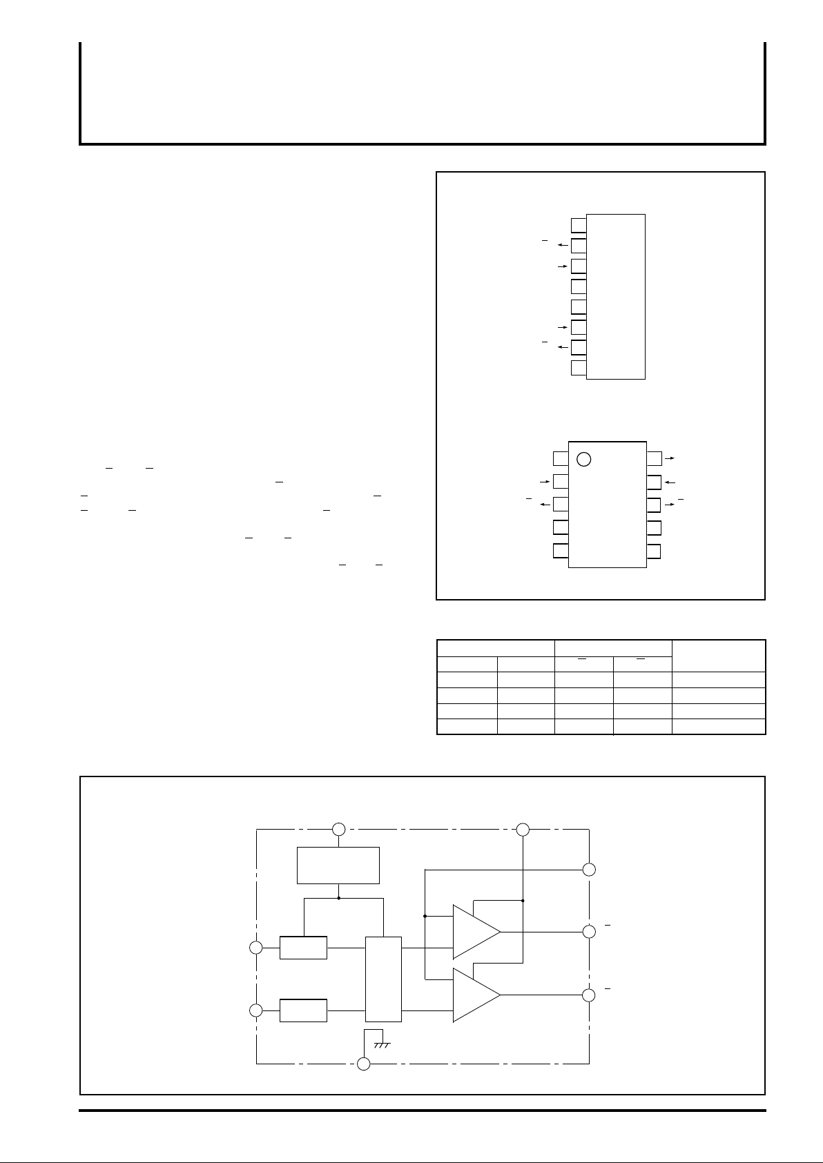
PIN CONFIGURATION(TOP VIEW
Input 1
control
Input 2
supply
IN2
VCC’
NC
GND
VZ
O
VCC
IN
IN2
VCC’
1
O2
1
VZ
O1
1
2
3
4
5
1
2
3
M54641L
4
5
6
7
8
Outline 8P5
M54641FP
Outline 10P2-C
Power supply
Output 2
Output voltage
Output 1
Output power
Output voltage
control
Input 2
Output 1
Output power
supply
LOGIC TRUTH TABLE
Input
1
IN
L
H
L
H
IN
2
L
L
H
H
O
“OFF”
state
H
L
L
Output
1
O
“OFF”
state
H
GND
6
7
IN
8
O2
9
VCC
NC
10
NC: no connection
2
No operation of IC
ex
L
Forward rotation
Reverse rotation
L
1
Input 1
Output 2
Power supply
Remarks
Brake
BLOCK DIAGRAM
Input 1
Input 2 IN2
Power supply
V
CC
Constant voltage
source
1
IN
Input
circuit
Control
circuit
Input
circuit
GND
Output power supply
Output
circuit
Output
circuit
V
CC’
Z
Output voltage controlV
Output 2O2
Output 1O1

Bi-DIRECTIONAL MOTOR DRIVER WITH BRAKE FUNCTION
Though the IC is equipped with a thermal shutdown circuit for
prevention against thermal breaking, the threshold temperature is
set to 100°C min. Set the driving current in such a way that this
thermal shutdown circuit cannot operate during normal operation.
INPUT/OUTPUT CIRCUIT
1 2
VCC
MITSUBISHI <CONTROL / DRIVER IC>
M54641L/FP
V
Output circuitInput circuit
Z
VCC’
Output
INInput
15k1k
GND
ABSOLUTE MAXIMUM RATINGS (Ta=25˚C, unless otherwise noted)
Symbol
VCC
VCC’
VI
VO
IO(max)
IO
Pd
j Junction temperature
T
Topr
Tstg
Supply voltage
Output Supply voltage
Input voltage
Output voltage
Allowable motor rush current
Continuous output current
Power dissipation
Operating temperature
Storage temperature
Parameter
V
I<VCC
t
OP =10ms: cycle time 0.2HZ or less
a = 60˚C(M54641L)
T
Conditions
RECOMMENDED OPERATING CONDITION (Ta = 25˚C, unless otherwise noted)
Symbol
V
O
I
VIH
VIL
CC
Supply voltage
Output current
“H” input voltage
“L” input voltage
tS Motor braking interval
S
T
Operation temperature of thermal
protection circuit (junction temperature)
Parameter
Conditions Unit
Min.
3.0
10
100
4
0
Ratings
-0.5 – +12
-0.5 – +20
0 – VCC
– VCC’+2.5
-0.5
±800
±150
-10
-55
Limits
570
100
– 60
– 125
Typ.
5
100
120
GND
Max.
10
±100
VCC
0.6
Unit
V
V
V
V
mA
mA
mW
˚C
˚C
˚C
V
mA
V
V
ms
˚C

MITSUBISHI <CONTROL / DRIVER IC>
Bi-DIRECTIONAL MOTOR DRIVER WITH BRAKE FUNCTION
ELECTRICAL CHARACTERISTICS (Ta=25˚C, VCC = 5V, unless otherwise noted)
Symbol
I
O(leak)
VOH
VOL
VO1-O2
II
ICC
Parameter
Output leak current
“H” output saturation voltage
“L” output saturation voltage
Voltage between outputs (1)
and (2) (Voltage across Motor)
Input voltage
Supply current
CC’ = 20V
V
V
Z: Open
CC’ = 12V
V
V
Z: Open
CC’ = 12V
V
V
Z: Open
VCC’ = 12V
V
Z = 7V
V
CC’ = 12V
CC = 10V
V
V
CC’ = 12V
Output OPEN
Test conditions
VI = 3V
V
I = 5V
V
O = 20V
V
O = 0V
OH = -50mA
I
I
OH = -100mA
OH = 50mA
I
I
OH = 100mA
I
O = ±100mA
Output open
In “OFF” state
Forward rotation or
reverse rotation
Braking
Min.
10.2
10.0
6.3
M54641L/FP
Limits
Typ.
10.5
10.4
0.1
0.2
7.0
100
240
1.2
4.5
7.5
Max.
100
-100
0.3
0.4
7.7
180
380
3.0
8.0
12.0
Unit
µA
V
V
V
µA
mA
TYPICAL CHARACTERISTICS
Thermal Derating (M54641L)
(Absolute Maximum Rating)
sec
t = 20
t =
0
0
25 50 60 75 100
Ambient Temperature Ta (˚C)
“H” Output Saturation
Characteristics
Ta = 25˚C
CC’ = 12V
V
Z = Open
V
Power Dissipation Pd(max) (W)
1.6
1.4
1.2
1.0
0.8
0.6
0.4
0.2
-200
-150
Condition
t = 10sec
• With basic installation (epoxy board of 5cm x 5cm x 0.8mmt with copper foil on a single
side)
• t : Power apply time
Thermal Derating (M54641FP)
(Absolute Maximum Rating)
0.8
0.6
0.4
0.2
Power Dissipation Pd(max) (W)
0
0
25 50 60 75 100
Ambient Temperature Ta (˚C)
“L” Output Saturation
Characteristics
200
Ta = 25˚C
CC’ = 12V
V
Z = Open
V
150
-100
-50
“H” Output Current IOH (mA)
0
0 0.2 0.4 0.6 0.8 1.0 1.2 1.4 1.6 1.8 2.0
“H” Output Voltage VCC’-VOH (V)
100
50
“L” Output Current IOL (mA)
0
0 0.1 0.2 0.3 0.4 0.5
“L” Output Voltage VOL (V)
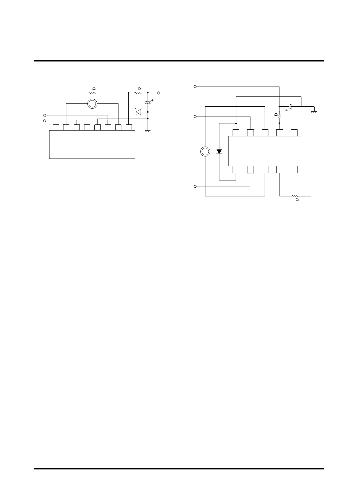
APPLICATION EXAMPLE
2
M
1
IN
IN2
87654321
M54641L
MITSUBISHI <CONTROL / DRIVER IC>
M54641L/FP
Bi-DIRECTIONAL MOTOR DRIVER WITH BRAKE FUNCTION
3
B
V
10 – 100µF
VB
IN1
3
10 9 8 7 6
M
M54641FP
10 – 100µF
CAUTIONS
Since the thermal protection function of this IC may not work in
abnormal status (oscillation, low supply voltage, output shortcircuit, etc.), check the operation in the IC installation status when
using this function.
When the motor back electromotive force is large with the brakes
applied, for example, malfunction may occur in internal parasitic Di.
If flyback current of 1A or more flows, add Schottky Di to the
portion between the output and the GND.
When the IC is used at a high speed for PWM, etc., note that
switching of output results in delay of approx. 10µs.
IN2
1
2
3 4 5
2
 Loading...