


MITSUBISHI <CONTROL / DRIVER IC>
)
y
M54617P
LAN TRANSCEIVER
DESCRIPTION
The M54617P is an integrated circuit for two-wire system LAN
transceivers in compliance with J1850.
It has a built-in function detecting bus-line abnormality, and allows
ERR signal to turn to “L” in case of abnormality. In addition, the
selector permits the output of normal bus signal.
Turning the standby signal to “L” provides a low current dissipation
status, when both BUS(+) and BUS(-) of the driver are turned OFF.
Further, inputting “H” level to ERR pin when in the standby mode
allows error output to be reset.
FEATURES
●Compliance with SAE J1850 standards
●Built-in function detecting bus-line abnormality
APPLICATION
LAN transceivers in general and other communication transceivers
(The M59330P having the same function is available as a vehicleloaded LAN transceiver).
PIN CONFIGURATION (TOP VIEW)
Data input
Standb
Error I/O
Data output
input
STB
ERR
RX
TX
1
2
3
4
Outline 8P4
M54617P
8
7
6
5
VDD
BUS(+
BUS(-)
SS
V
Power supply
Bus-line I/O
GND
BLOCK DIAGRAM
1
Data input
Standby
input
Error I/O
Data output R
TX
STB
ERR
2
3
X
4
Standby control
circuit
Abnormality
detection circuit
Selector
Output control
circuit
Overcurrent
detection circuit
Driver
Driver
BUS (+) signal
detection
circuit
BUS (-) signal
detection
circuit
Filter
8
7
6
5
DD
V
BUS (+)
BUS (-)
V
SS
Power
supply
Bus-line
I/O
GND

MITSUBISHI <CONTROL / DRIVER IC>
FUNCTION
Pin function
Pin No. Pin name I/O Function
1
TX Input Data signal input pin
2
STB Input
3
ERR I/O
Standby signal input pin
L: standby mode, H: normal operation
Error signal output pin and error reset input pin
“L” level output when abnormal transmission route is detected
Error reset with “H” level input when in the standby mode
M54617P
LAN TRANSCEIVER
4
5
6
7
8
X Output Signal output pin from transmission route
R
SS Input Grounding pin
V
BUS(-) I/O Signal output pin to transmission route and signal input pin from transmission route (negative logic)
BUS(+) I/O Signal output pin to transmission route and signal input pin from transmission route (positive logic)
DD Input
Power supply pinV
ABNORMALITY DETECTION OF TRANSMISSION
ROUTE AND COMMUNICATION FUNCTION
The M54617P uses its driver overcurrent detection function and
transmission signal logic abnormality function to perform the
abnormality detection of the transmission route, and outputs error
signal (ERR(3 pin) = “L”).
In addition, switching the signal that is output to Rx pin (pin 4)
according to the abnormality occurrence status permits
communication after abnormality has occurred.
(1) Overcurrent detection
BUS(+) pin (pin 7) and BUS(-) pin (pin 6) drivers of M54617P are
equipped with an overcurrent detection circuit. When overcurrent
flows to a driver, the driver is turned OFF to output error signal
(ERR (pin 3) = “L”). Once an overcurrent is detected, the driver
maintains the OFF status until the error is reset.
In addition, each driver of BUS(+) pin (pin 7) and BUS(-) pin (pin 6)
is independent, and both may be turned OFF depending upon the
abnormality occurrence status.
A built-in filter for the prevention of malfunction due to overcurrent
when the driver is turned ON does not permit the detection of the
overcurrent status for a short time (several hundred ns). Detection
current is set to about 180mA.
(3) Communication function
The M54617P ordinarily outputs the differential signals of BUS(+)
(pin 7) and BUS(-) (pin 6). When abnormality is detected, signals to
be output to Rx pin (pin 4) are switched according to the status.
When overcurrent is detected, the driver or the transmission route
in which overcurrent is detected is considered abnormal, and error
signal is output, and concurrently the signal of another
transmission route is output to Rx output (pin 4).
As described in the above section (1), both drivers are turned OFF
in some cases. In these cases, Rx output (pin 4) is fixed to “L”.
When logic abnormality is detected, error signal (ERR (pin 3) = “L”)
is output, and concurrently Rx output (pin 4) is turned to “L”. After
error signal is output, the transmission route in which the edge of
transmission signals is detected is considered normal, and such
signal is output to Rx output (pin 4).
In switching operation of error signal output and Rx output the
priority is given to overcurrent detection over logic abnormality
detection.
(2) Logic abnormalitydetection
The M54617P transmission signals operate in the opposite phase
to each other, and abnormal transmission route is detected by
comparing these signals. Upon comparing respective signals after
a set time on the basis of the edge of transmission routes BUS(+)
and BUS(-), any disagreement is regarded as abnormal
transmission, and error signal (ERR (pin 3) = “L”) is output. In order
to be well timed with that edge as a new standard, abnormality is
detected when signal disagreement continues for more than a set
time. Setting time is set to about 4.2µs.
Logic abnormality detection does not cope with more than one
error mode.
Detection of logic abnormality alone does not allow the driver to be
turned OFF. Abnormality detection allows the driver to be turned
OFF only when overcurrent is detected.

Table 1. Abnormalitymode and abnormalitydetection function
Abnormality mode Error output
1
2
BUS(+)
3
4
5
BUS(-)
6
7
BUS(+) and BUS(-) short
GND short
VDD short
Open
GND short
V
DD short
Open
Yes Yes
Yes Yes
Yes Yes
Yes Yes
Yes Yes
Yes Yes
Yes No
Communication after
abnormality is detected
MITSUBISHI <CONTROL / DRIVER IC>
M54617P
LAN TRANSCEIVER
Abnormality
detection method
(2)
(1), (2)
(2)
(1), (2)
(2)
(2)
(1)
ERROR RESET
Error output of the M54617P can be reset by turning to the standby
mode (STB pin (pin 2) = “L”), followed by inputting “H” level to ERR
pin (pin 3). In this case, all operations are cleared that relate to
abnormality detection including overcurrent detection and switching
of Rx output.
I/O EQUIVALENT CIRCUIT
Tx and STB input
1
STANDBY MODE
The M54617P can be set to the low current dissipation mode by
turning STB pin (pin 2) to level “L”.
Standby mode does not allow the driver and overcurrent detection
function to be operated, but logic abnormality detection function
operates, which permits detection other than abnormality relating
to overcurrent detection. However, it provides error signal output
only, but no switching of Rx output signal.
Rx output when in the standby mode outputs the logic sum of
BUS(+) and BUS(-) signals.
ERR I/O
2
3
Rx output
BUS(+) and BUS(-) I/O
4
BUS (+)
BUS (-)
Filter time constant
RC = 110E-9 (standard)

MITSUBISHI <CONTROL / DRIVER IC>
)
)
M54617P
LAN TRANSCEIVER
ABSOLUTE MAXIMUM RATINGS(Ta = 25°C unless otherwise noted
Symbol Unit
DD Supply voltage
V
VI
VO
IO
Pmax
Tstg
Note: All voltages shall be based on VSS pin of the circuit, the max. and min. values be indicated in the absolute values, and the directions
Input voltage
Output voltage
Driver output current
Allowable power dissipation
Storage temperature
of the current be positive when flowing into the circuit and negative (“-” symbol) when flowing out of the circuit.
Parameter
BUS(+)
BUS(-)
Conditions
Min. Typ. Max.
-0.3 6.5
-0.3 V
RECOMMENDED OPERATING CONDITIONS(Ta = 25°C unless otherwise noted
Symbol Unit
DD Supply voltage
V
RBUS
CBUS
opr
BUS resistance
BUS capacitance
Operating temperatureT
Parameter
Conditions
Transmission rate = 41.6Kbps
Transmission rate = 125Kbps
Transmission rate = 41.6Kbps,
RBUS = 378Ω
Transmission rate = 125Kbps,
RBUS = 378Ω
Ratings
DD+0.3
DD+0.3
-50
Limits
Min. Typ.
4.75 5.25
105
105
Max.
10000
3000
50
V
V
V-0.3 V
mA
mW200
°C-50 125
V
Ω
pF
°C-20 75

MITSUBISHI <CONTROL / DRIVER IC>
M54617P
LAN TRANSCEIVER
ELECTRICAL CHARACTERISTICS (Ta = 25°C and VDD = 5.0V when in normal operation unless otherwise noted)
Symbol Parameter
DD1
I
IDD2
IDD3
VTH1
VTH2
VTL
VHYSL
VCIN
VHYSB
IIPP1
IIDP1
IIPP2
IIDP2
IIPM1
IIDM1
IIPM2
IIDM2
VDROP1
VDROP2
VOH1
VOL1
VOH2
IPD
CI1
CI2
VTH1
Supply current 1
Supply current 2
Supply current 3
“H” input threshold voltage 1
“H” input threshold voltage 2
“L” input threshold voltage
Hysterisis width
BUS input voltage range
Input hysterisis width
BUS(+) leakage current 1
BUS(+) leakage current 2
BUS(+) leakage current 3
BUS(+) leakage current 4
BUS(-) leakage current 1
BUS(-) leakage current 2
BUS(-) leakage current 3
BUS(-) leakage current 4
Driver and drop voltage
“H” output voltage 1
“L” output voltage 1
“H” output voltage 2
ERR pulldown current
Input capacitance 1
Input capacitance 2
Grounding offset voltage
Conditions
RBUS = 105Ω,
X = “L”, STB = “H”
T
RBUS = 105Ω,
T
X = “H”, STB = “H”
RBUS = 105Ω,
X = STB = “H”
T
ERR
T
X, STB
T
X, STB
T
X, STB
BUS(+), BUS(-)
BUS(+) and BUS(-) differential input
When the power supply is turned OFF
(V
DD = 0V), BUS(+) = 0V
When the power supply is turned OFF
DD = 0V), BUS(+) = 5V
(V
When the power supply is turned ON
BUS(+) = 0V
When the power supply is turned ON
BUS(+) = 5V
When the power supply is turned OFF
(V
DD = 0V), BUS(-) = 5V
When the power supply is turned OFF
DD = 0V), BUS(-) = 0V
(V
When the power supply is turned ON
BUS(-) = 5V
When the power supply is turned ON
BUS(-) = 0V
IBUS(+) = -50mA
IBUS(-) = +50mA
R
X pin IOH = -1mA
R
X pin IOL = +1mA
ERR pin I
ERR pin V
OH = -1mA
OH = 3.0V
When the power supply is turned OFF
(V
DD = 0V)
When the power supply is turned ON
Between 2 nodes
Min. Typ. Max.
Limits
5.0 mA
55 mA
200 µA
2.2 3.2 V
2.3 3.5 V
1.6 2.8 V
0.4 1.0 V
V
SS VDD-2.0 V
70 300 mV
100 µA
100 µA
-20 µA
100 µA
100 µA
100 µA
20 µA
100 µA
1.5
0.6
4.5 5.0 V
0.6 V
4.5 5.0 V
350
700 µA
150 pF
150 pF
0.5 V
Unit
V

MITSUBISHI <CONTROL / DRIVER IC>
)
M54617P
LAN TRANSCEIVER
TIMING CHARACTERISTICS(Ta = 25°C and VDD = 5.0V when in normal operation unless otherwise noted
Symbol Parameter
T
dTBr
TdTRr TX → RX rise delay time
TdTRf TX → RX fall delay time
Conditions
CBUS = 10000pF,
RBUS = 378Ω
Transmission rate = 41.6Kbps
CBUS = 10000pF,
RBUS = 378Ω
Transmission rate = 41.6Kbps
CBUS = 10000pF,
RBUS = 378Ω
Transmission rate = 41.6Kbps
Min. Typ. Max.
Limits
0.25 µsTX → BUS output delay time
0.6 µs
3.0 µs
Unit
dBRr BUS → RX rise delay time
T
dBRf BUS → RX fall delay time
T
TWS STB input minimum pulse width
T
SS STB input setup time
ThS STB input holding time
T
WE ERR input pulse width
Transmission rate = 41.6Kbps
Transmission rate = 41.6Kbps
Standby mode
At error reset
At error reset
At error reset
3.0
1.0
100
200
0.35 µs
0.33 µs
µs
µs
ns
ns
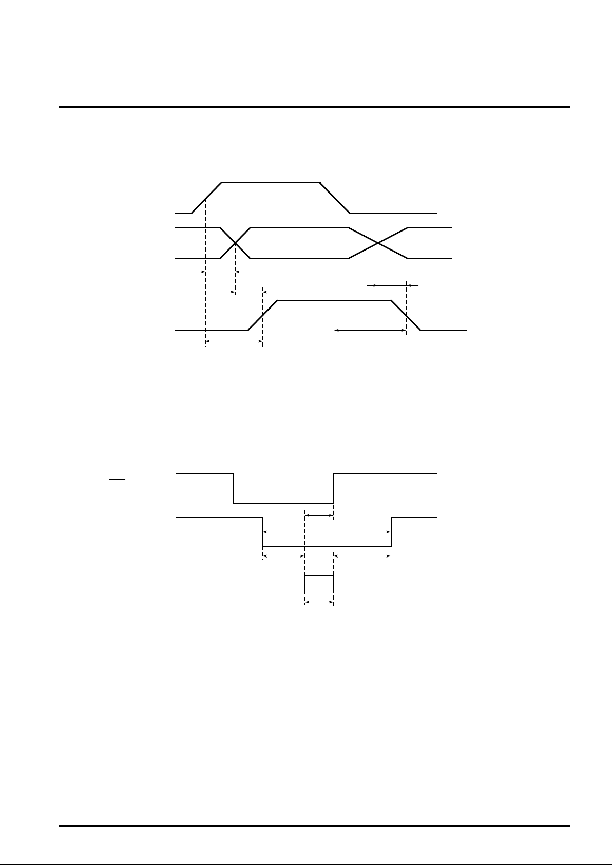
TIMING DIAGRAM
g
g
r
Timin
waveform
TX
BUS (-)
BUS (+)
RX
MITSUBISHI <CONTROL / DRIVER IC>
M54617P
LAN TRANSCEIVER
dTB
T
TdBRr
TdTRr
TdBRf
TdTRf
Error reset timin
ERR
(output)
STB
ERR
(reset input)
TsS ThS
TdE*= about 20ns (reference value)
dE*
T
TwE
TwS
High impedance

MITSUBISHI <CONTROL / DRIVER IC>
y)
(-)
LAN TRANSCEIVER
APPLICATION EXAMPLE(This is only an example, so it allows more examination if necessar
Transmission route connection example
M54617P
RL
RL
Peripheral circuit example
VDD
Controller
(M64100TFP)
Microcomputer
BUS(+) BUS(-)
M54617P
Peripheral controller
(M64100TFP) and
microcomputer
circuits
Board 1
10k
10k
Transmission route (twist pair cable)
1
2
3
4
M54617P
8
7
6
5
BUS(+) BUS(-)
M54617P
Peripheral controller
(M64100TFP) and
microcomputer
circuits
Board n
0.1µF
RL
V
Z = 7V Zenor
RL
RL
10µF
L
R
BUS (+)
BUS
• Use of Zenor diode in the range of Vz = 7V is recommended for surge protection.
• Installation of external capacitance is recommended between the power supply pin and GND in order to prevent
malfunction due to noise, etc.
• In the example given, terminal resistor is connected to the edge of transmission route in the transmission route
connection, but the method of connecting terminal resistor to each node is recommended. In this case, pay attention to
the total terminal resistance value of the transmission route.
 Loading...