Mitsubishi M54544AL Datasheet

MITSUBISHI <CONTROL / DRIVER IC>
)
M54544AL
Bi-DIRECTIONAL MOTOR DRIVER
WITH BRAKE FUNCTION AND THERMAL SHUT DOWN FUNCTION
DESCRIPTION
The M54544AL is a semiconductor integrated circuit that is
capable of directly driving a smallsize bi-directional motor rotating
in both forward and reverse directions.
FEATURES
●Wide range of operating voltage (VCC=4 – 16V)
●Possible direct driving with TTL, PMOS and CMOS IC outputs
●Low output saturation voltage (large voltage across motors)
● Built-in clamp diode
● Large output current drive (IO(max)=±1.5A)
● Provided with brake function
●Built-in thermal shutdown protection circuit
APPLICATION
Sound equipment such as tape deck and radio cassette, VTR, and
other general consumer appliances
FUNCTION
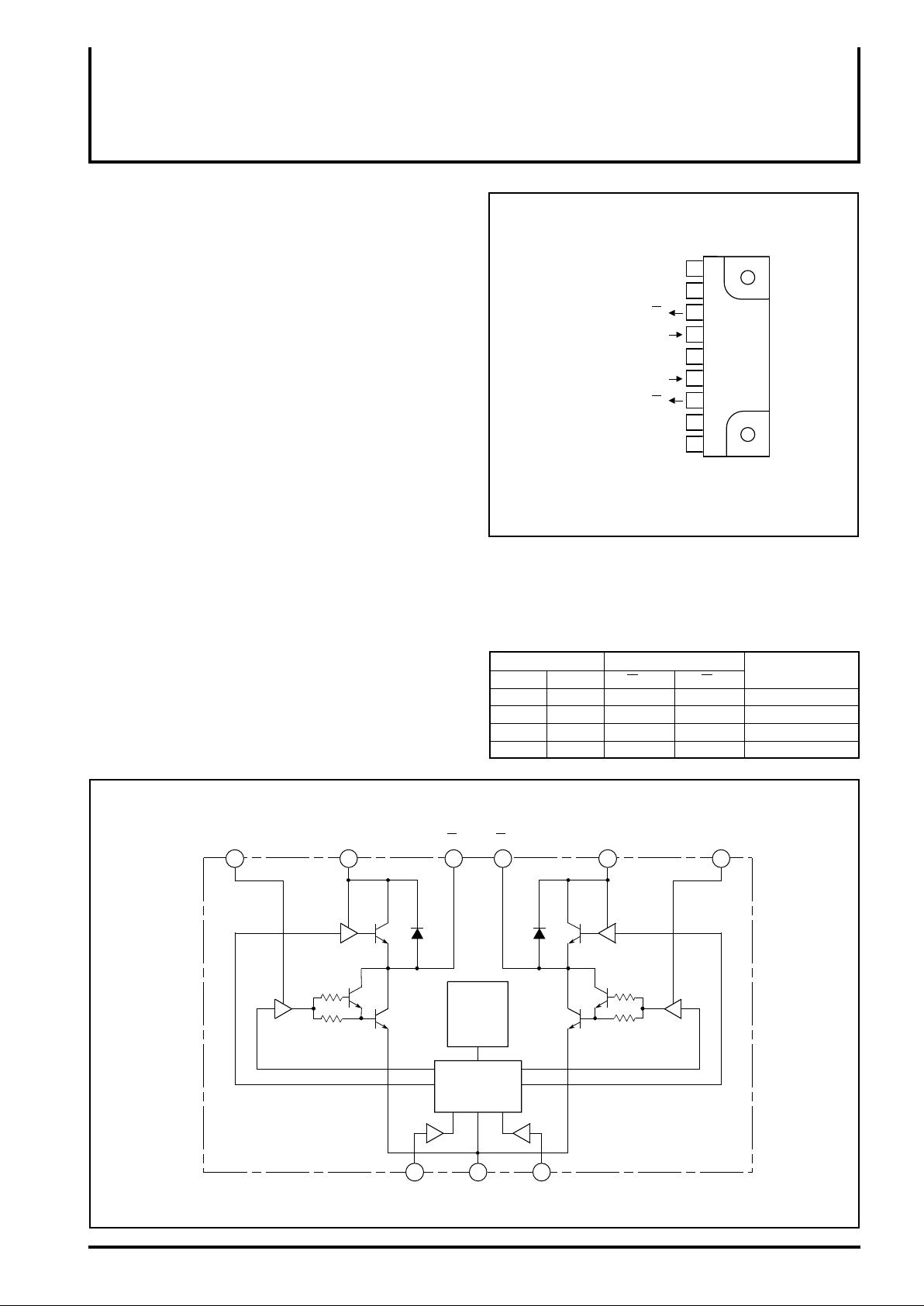
The M54544AL is an IC for driving a smallsize bi-directional motor
that rotates in both forward and reverse directions. When both
inputs 1 and 2 are set to low-level, outputs 1 and 2 are set to
“OFF”. When input 1 is set to high-level and input 2 is set to lowlevel, output 1 is set to high-level and output 2 is set to low-level
(forward rotation status). When input 1 is set to low-level and input
2 is set to high-level, output 1 is set to low-level and output 2 is set
to high-level (reverse rotation). When both inputs 1 and 2 are set to
high-level, both outputs 1 and 2 are set to low-level (brake status).
The power supply (VCC) to the control circuit and the power supply
(VCC’) for output are independently provided. The rotating speed of
the motor can be therefore changed by using VCC and VCC’ as
different power supplies and by making VCC or VCC’ variable.
If the motor resistance is high (light load and small driving current:
tens of mA), and VCC is larger than VCC’, current does not flow
backward from the VCC pin to VCC’ pin.
PIN CONFIGURATION(TOP VIEW
O
IN
IN
O1
CC2
2
1
2
1
2
3
M54544AL
4
5
6
7
8
9
Outline 9P9
Power supply 1
Output power supply 1
Output 2
Input 1
Input 2
Output 1
Output power supply 2
Power supply 2
VCC1
VCC’1
GND
VCC’2
V
In addition, built-in thermal protection circuit protects the IC from
thermal destruction in case of abnormal condition such as motor
blocking.
LOGIC TRUTH TABLE
Input Output
IN
1 IN2
LL
HL
LH
HH
O
“OFF” state “OFF” state
HL
LH
LL
1 O2
Remarks
No operation of IC
ex Forward rotation
Reverse rotation
Brake
BLOCK DIAGRAM
Output power supply 1 Output 1Power supply 1
VCC1
1 3 7 9
VCC’1
2 8
Output 2
O2
Input control
4 5 6
IN1
Input 1
O
Thermal
protection
circuit
circuit
GND
1
Output power supply 2
2
IN
Input 2
Power supply 2
CC’2
V
CC2
V

WITH BRAKE FUNCTION AND THERMAL SHUT DOWN FUNCTION
)
)
)
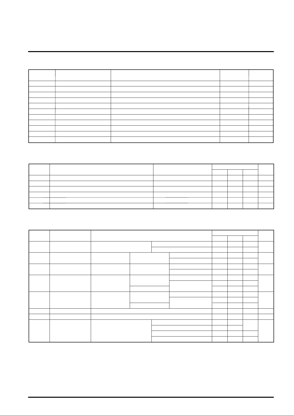
ABSOLUTE MAXIMUM RATINGS(Ta=25°C, unless otherwise noted
MITSUBISHI <CONTROL / DRIVER IC>
M54544AL
Bi-DIRECTIONAL MOTOR DRIVER
Symbol
VCC(1)
VCC(2)
VCC’
V
I
VO
IO(max)
IO(1)
IO(2)
Pd
Topr
Tstg
Supply voltage(1)
Supply voltage(2)
Output supply voltage
Input voltage
Output voltage
Allowable motor rush current
Continuous output current(1)
Continuous output current(2)
Power dissipation
Operating temperature
Storage temperature
Parameter Conditions
With an external heat sink (3000mm
t
op=10ms : cycle time 0.2Hz or less
With an external heat sink (3000mm
Ta=75˚C
2
x 1.5mm)
2
x 1.5mm)
RECOMMENDED OPERATING CONDITION(Ta=25°C, unless otherwise noted
Symbol Conditions
CC
V
I
O
VIH
VIL
tB
tj(shut)
Supply voltage
Output current
“H” input voltage
“L” input voltage
Motor braking interval
Thermal shutdown temperature
Parameter
VCC ≥ 7V
Ratings
-0.5 – +16
-0.5
– +20
-0.5
– +16
0 – VCC
– VCC’+2.5
-0.5
±1.5
±330
±600
1.15
-10
– 75
– 125
-55
Limits
Min. Typ. Max.
12
4
15
±300
V
CC
0.4
10
2
0
100
150
Unit
V
V
V
V
V
A
mA
mA
W
°C
°C
Unit
V
mA
V
V
ms
˚C
ELECTRICAL CHARACTERISTICS(Ta=25°C, unless otherwise noted
Symbol Test conditions
O(leak)
I
VOH(1)
V
OH(2)
OL(1)
V
OL(2)
V
IH(1)
I
IH(2)
I
I
CC
Parameter
Output leak current
“H” output saturation
voltage(1)
“H” output saturation
voltage(2)
“L” output saturation
voltage(1)
“L” output saturation
voltage(2)
“H” input current(1)
“H” input current(2)
Supply current
CC=VCC’=20V
V
VI1=VI2=0V
V
CC=VCC’=12V
V
CC=VCC’=12V
V
CC=VCC’=12V
V
I1=2V
VI2=0V
V
I1=0V
VI2=2V
V
I1=0V
VI2=2V
VI1=VI2=2V
V
I1=2V
CC=VCC’=12V
V
VI2=0V
VI1=VI2=2V
VCC=VCC’=12V, VI1=2V, VI2=0V
VCC=VCC’=12V, VI1=0V, VI2=2V
V
CC=VCC’=16V
Output open
O=20V
V
VO=0V
I
OH(1)=-200mA
I
OH(1)=-500mA
I
OH(2)=-200mA
I
OH(2)=-500mA
OL(1)=200mA
I
IOL(1)=500mA
IOL(2)=200mA
IOL(2)=500mA
VI1=2V, VI2=0V
I1=0V, VI2=2V
V
VI1=VI2=2V
V
I1=VI2=0V
Limits
Min. Typ. Max.
100
-100
50
50
11.2
11.1
11.2
11.1
0.2
0.95
0.95
0.2
0.95
0.95
0.5
1.35
1.35
0.5
1.35
1.35
120
120
10.8
10.7
10.8
10.7
15
20
4
Unit
µA
V
V
V
V
µA
µA
mA
 Loading...