

MITSUBISHI SEMICONDUCTOR <TRANSISTOR ARRAY>
M54532P/FP
4-UNIT 1.5A DARLINGTON TRANSISTOR ARRAY WITH CLAMP DIODE
DESCRIPTION
M54532P and M54532FP are four-circuit Darlington transistor arrays with clamping diodes. The circuits are made of
NPN transistors. Both the semiconductor integrated circuits
perform high-current driving with extremely low input-current
supply.
FEATURES
Á High breakdown voltage (BV
CEO ≥ 50V)
Á High-current driving (Ic(max) = 1.5A)
Á With clamping diodes
Á Wide operating temperature range (Ta = –20 to +75°C)
APPLICATION
Drives of relays and printers, digit drives of indication elements (LEDs and lamps), and power amplification
FUNCTION
The M54532P and M54532FP each have four circuits consisting of NPN Darlington transistors. They have resistance
of 340Ω between input transistor bases and input pins. A
clamping diode is provided between each output pin (collector) and COM pin. The output transistor emitters are all connected to the GND pin.
The collector current is 1.5A maximum. Collector-emitter
supply voltage is 50V maximum.
The M54532FP is enclosed in a molded small flat package,
enabling space-saving design.
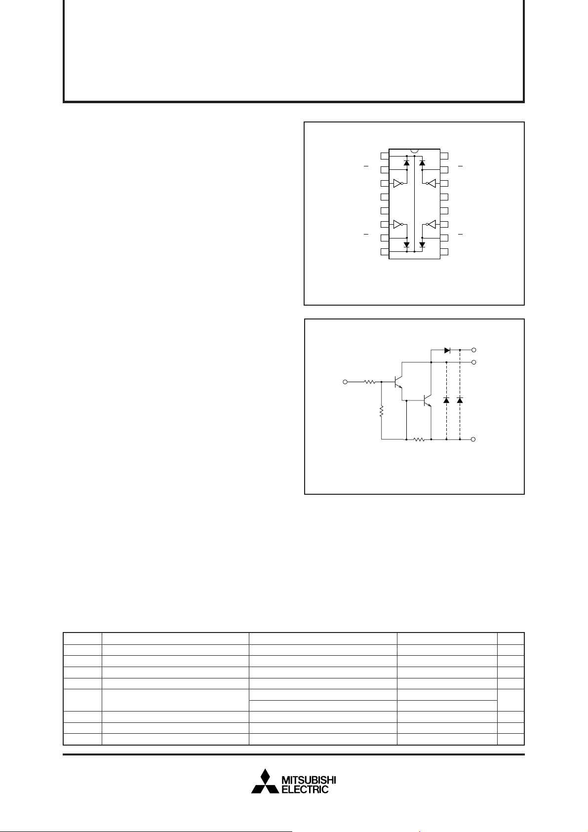
PIN CONFIGURATION
1
COMCOMMON
OUTPUT1
INPUT1
INPUT2 IN2→
OUTPUT2
2
O1←
IN1→
3
4
GND GND
5
6
7
O2←
COMCOMMON
8
16P4(P)
Package type 16P2N-A(FP)
NC
16
→O4
15
14
13
12
11
10
9
OUTPUT4
←IN4
INPUT4
←IN3
INPUT3
→O3
OUTPUT3
NC
NC : No connection
CIRCUIT DIAGRAM
INPUT
The diode, indicated with the dotted line, is parasitic, and cannot
be used.
340
5.5K
3K
The four circuits share the COM and GND.
COM
OUTPUT
GND
Unit : Ω
ABSOLUTE MAXIMUM RATINGS (Unless otherwise noted, Ta = –20 ~ +75°C)
Symbol Parameter Conditions Unit
VCEO
IC
VI
VR
IF
Pd
Topr
Tstg
Collector-emitter voltage
Collector current
Input voltage
Clamping diode reverse voltage
Clamping diode forward current
Power dissipation
Operating temperature
Storage temperature
Output, H
Current per circuit output, L
Pulse Width ≤ 10ms, Duty Cycle ≤ 5%
Pulse Width ≤ 100ms, Duty Cycle ≥ 5%
Ta = 25°C, when mounted on board
Ratings
–0.5 ~ +50
1.5
–0.5 ~ +10
50
1.5
1.25
1.92(P)/1.00(FP)
–20 ~ +75
–55 ~ +125
Aug. 1999
V
A
V
V
A
W
°C
°C
MITSUBISHI SEMICONDUCTOR <TRANSISTOR ARRAY>
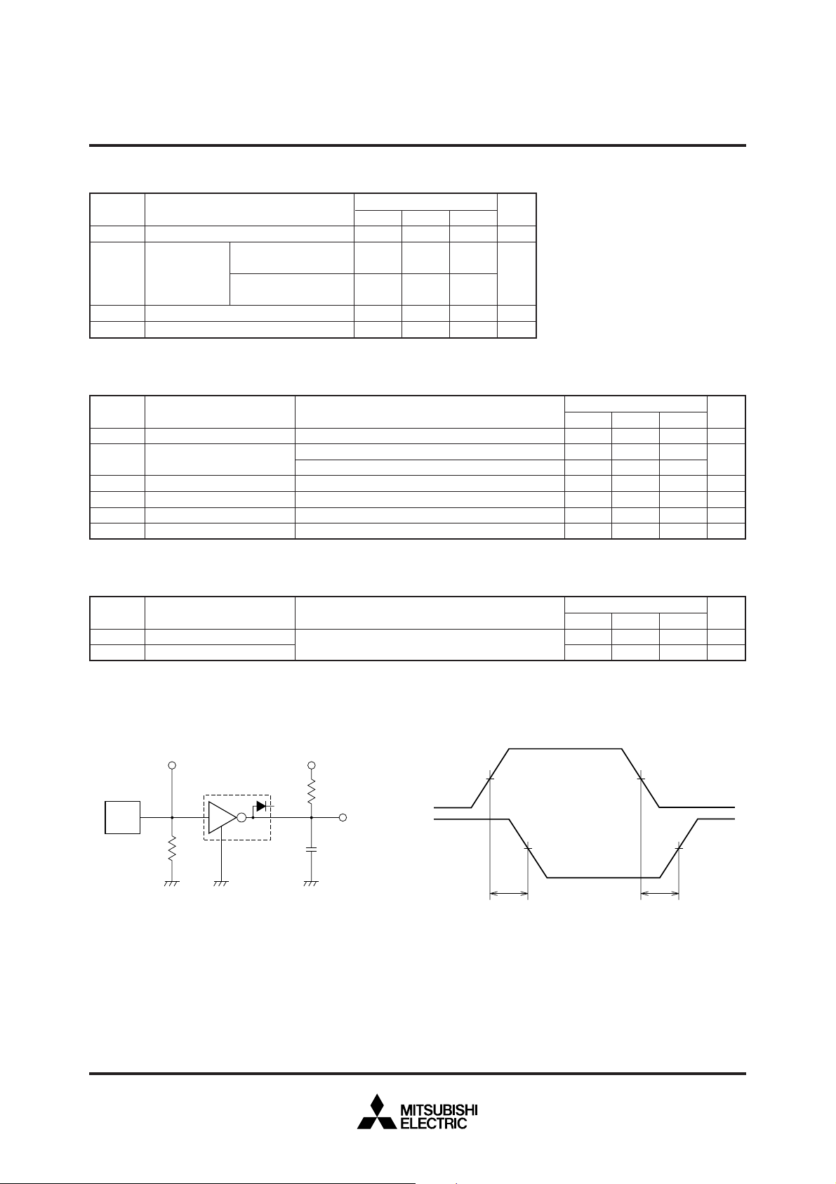
ton
50% 50%
50% 50%
toff
INPUT
OUTPUT
M54532P/FP
4-UNIT 1.5A DARLINGTON TRANSISTOR ARRAY WITH CLAMP DIODE
RECOMMENDED OPERATING CONDITIONS (Unless otherwise noted, Ta = –20 ~ +75°C)
ParameterSymbol
V
I
C
VIH
VIL
O
Output voltage
Collector current
(Current per 1 circuit when 4 circuits
are coming on simultaneously)
“H” input voltage
“L” input voltage
Duty Cycle
P : no more than 4%
FP : no more than 2%
Duty Cycle
P : no more than 18%
FP : no more than 9%
ELECTRICAL CHARACTERISTICS (Unless otherwise noted, Ta = –20 ~ +75°C)
Symbol UnitParameter Test conditions
V
(BR) CEO
VCE (sat)
II
IR
VF
hFE
+ : The typical values are those measured under ambient temperature (Ta) of 25°C. There is no guarantee that these values are obtained under any
conditions.
Collector-emitter breakdown voltage
Collector-emitter saturation voltage
Input current
Clamping diode reverse current
Clamping diode forward voltage
DC amplification factor
ICEO = 100µA
I = 2mA, IC = 1.25A
I
I = 2mA, IC = 0.7A
I
I = 3V
V
R = 50V
V
F = 1.25A
I
CE = 4V, IC = 1A, Ta = 25°C
V
Limits
min typ max
0
0
0
3
0
—
—
—
50
1.25
0.7
—
—
0.4
Unit
V
A
6
V
V
Limits
+
1.3
1.1
1.6
max
—
2.2
1.7
8.5
5
100
2.3
—
V
V
mA
µA
V
—
min typ
50
—
—
—
—
—
800
7000
—
—
SWITCHING CHARACTERISTICS (Unless otherwise noted, Ta = 25°C)
Symbol UnitParameter Test conditions
ton
toff
Turn-on time
Turn-off time
L = 15pF (note 1)
C
TIMING DIAGRAMNOTE 1 TEST CIRCUIT
OPEN
O
V
R
L
OUTPUT
L
INPUT
Measured device
PG
50Ω C
(1) Pulse generator (PG) characteristics : PRR = 1kHz,
tw = 10µs, tr = 6ns, tf = 6ns, Z
V
P
= 3V
(2) Input-output conditions : RL = 8.3Ω, VO = 10V
(3) Electrostatic capacity C
connections and input capacitance at probes
P-P
O
= 50Ω
L
includes floating capacitance at
Limits
min typ max
—
—
10
500
—
—
ns
ns
Aug. 1999

TYPICAL CHARACTERISTICS
Thermal Derating Factor Characteristics
Ambient temperature Ta (°C)
M54532FP
M54532P
Power dissipation Pd (W)
0
0
0.5
1.0
1.5
2.0
25 50 75 100
II = 2mA
Output Saturation Voltage
Collector Current Characteristics
Output saturation voltage V
CE
(sat) (V)
0
0
0.5
1.0
Ta = –20°C
Ta = 25°C
Ta = 75°C
1.5
2.0
0.5 1.0 1.5 2.0
Collector current Ic (A)
Duty-Cycle-Collector Characteristics
(M54532P)
Duty cycle (%)
•The collector current values
represent the current per circuit.
•Repeated frequency ≥ 10Hz
•The value in the circle represents the
value of the simultaneously-operated circuit.
•Ta = 25°C
0
0
0.5
1.0
1.5
2.0
➀
➁
➂
➃
20 40 60 80 100
Collector current Ic (A)
Duty cycle (%)
0
0
0.5
1.0
1.5
2.0
➀
➁
➂
➃
20 40 60 80 100
Collector current Ic (A)
Duty cycle (%)
0
0
0.5
1.0
1.5
2.0
➀
➁
➂
➃
20 40 60 80 100
Collector current Ic (A)
Duty cycle (%)
0
0
0.5
1.0
1.5
2.0
➀
➁
➂
➃
20 40 60 80 100
Collector current Ic (A)
Duty-Cycle-Collector Characteristics
(M54532P)
•The collector current values
represent the current per circuit.
•Repeated frequency ≥ 10Hz
•The value in the circle represents the
value of the simultaneously-operated circuit.
•Ta = 75°C
•The collector current values
represent the current per circuit.
•Repeated frequency ≥ 10Hz
•The value in the circle represents the
value of the simultaneously-operated circuit.
•Ta = 25°C
•The collector current values
represent the current per circuit.
•Repeated frequency ≥ 10Hz
•The value in the circle represents the
value of the simultaneously-operated circuit.
•Ta = 75°C
Duty-Cycle-Collector Characteristics
(M54532FP)
Duty-Cycle-Collector Characteristics
(M54532FP)
MITSUBISHI SEMICONDUCTOR <TRANSISTOR ARRAY>
M54532P/FP
4-UNIT 1.5A DARLINGTON TRANSISTOR ARRAY WITH CLAMP DIODE
Aug. 1999

MITSUBISHI SEMICONDUCTOR <TRANSISTOR ARRAY>
M54532P/FP
4-UNIT 1.5A DARLINGTON TRANSISTOR ARRAY WITH CLAMP DIODE
DC Amplification Factor
Collector Current Characteristics
5
10
7
VCE = 4V
5
3
FE
2
4
10
7
5
3
2
3
10
7
5
DC amplification factor h
3
2
2
10
1
10
23 57
Ta = 75°C
2
10
Collector current Ic (mA)
Input Characteristics
25
(mA)
I
20
15
Ta = –20°C
10
Input current I
5
0
246810
0
23 57
Ta = 25°C
Ta = 25°C
Ta = –20°C
3
10
23 57
Ta = 75°C
10
Grounded Emitter Transfer Characteristics
1.6
VCE = 4V
1.2
0.8
Ta = 75°C
0.4
Collector current Ic (A)
4
0
0
Ta = 25°C
Ta = –20°C
0.5 1.0 1.5 2.0
Input voltage V
I
(V)
Clamping Diode Characteristics
2.0
(A)
1.5
F
1.0
0.5
0
0
Ta = 75°C
0.5 1.0 1.5 2.0
Forward bias current I
Ta = 25°C
Ta = –20°C
Input voltage V
I
(V)
Forward bias voltage V
F
(V)
Aug. 1999
 Loading...