

MITSUBISHI <CONTROL / DRIVER IC>
)
(2)
(3)
(1)
(14)
(13)
M54125L/P
EARTH LEAKAGE CURRENT DETECTOR
DESCRIPTION
The M54125 is a semiconductor integrated circuit consisting of an
amplifier for high-speed earth leakage circuit breaker.
FEATURES
●Satisfies JIS C 8371
●Temperature-stable input current trigger threshold (VLKT = 9mV)
●Capable of detecting a lost phase on the neutral line
●Economical, low external component count
●Highly resistant to noise and power surges
●Wide operating temperature range (Ta = -20 – +80°C)
APPLICATION
High-speed earth-leakage circuit breakers
FUNCTION
The M54125 is a semiconductor integrated circuit for use in the
amplifier section of earth-leakage circuit breakers. It consists of a
differential amplifier, one-shot circuit, output circuit, current
regulator, waveform regulator and delay circuit. The following
description refers to the block diagram, application example, and
operational waveforms.
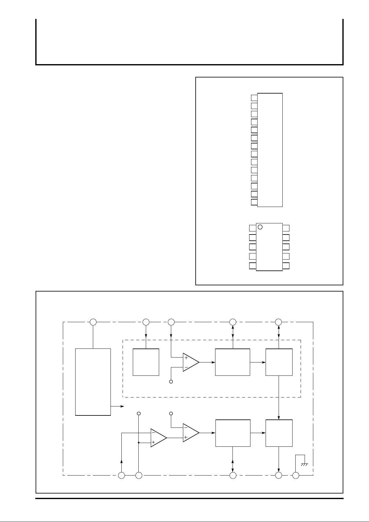
PIN CONFIGURATION(TOP VIEW
1
Output
Input
Input
Input
TD
ILK
VB
MM
OUT
GND
MM
OUT
GND
NC
TD
NC
WF
IBL
RX
NC
NC
VS
ILK
VB
→←
←
→←
→←
→
→
→
→
→
←
←
2
3
4
5
6
M54125L
7
8
9
10
11
12
13
14
Outline 14P5A
1
M54125P
2
3
4
10
9
←
←
8
→←
7
→←
65
Capacitor
Capacitor C
Capacitor CWF
External resistor
Bias voltage
Bias voltage
Capacitor
Output
N.C: no connection
VS
RX
External resistor
IBL
Input
WF
Capacitor C
Capacitor CTD
TD
WF
BLOCK DIAGRAM (Note: Pin No. in parentheses are of M54125L)
External
VS
(12) (9) (8) (7)
Voltage
regulator
VCC
resistor Input Capacitor C
RX IBL WF TD
Bias
current
source
Comparator
VBLT
VB
A • VLKT
A
Amplifier
Comparator
Wave-
form
regulator
One-shot
multi vibrator
Outline 10P2-C
WF Capacitor CWF
678910
(5)
Delay
circuit
Output
circuit
1 2 3
ILK VB MM OUT GND
Input Bias Capacitor Output
M54125L/P
4
5
MITSUBISHI <CONTROL / DRIVER IC>
)
)
µ
µ
EARTH LEAKAGE CURRENT DETECTOR
ABSOLUTE MAXIMUM RATINGS(Ta = -20 – 80°C unless otherwise noted
M54125L/P
Symbol
S
I
IS(SO)
∆VILK
VIBL
VOUT
Pd
Supply voltage
Supply surge current
ILK input voltage
IBL input voltage V
OUT applied voltage
Power dissipation
Parameter Conditions
Topr Operating temperature
T
stg
Note 1: I
Storage temperature
S(SG) current waveform, which is given in the following diagram, shall be one shot or less per minute.
Average supply current frequency
per cycle
(Note 1)
Pin VB serves as the voltage
reference
When external voltage is applied
IS(SG)
40
1
S
S
12mA
6mA
0mA
Ratings
0
0 – 12
-1.8
-0.3
-0.3
-20
-55
– 6
– +1.8
– 6
– 4
160
– 80
– 125
Unit
mA
mA
V
V
mW
°C
°C
RECOMMENDED OPERATING CONDITIONS(Ta = -20 – 80°C unless otherwise noted
Symbol
V
S
I
S
Supply voltage 12
Supply current
Parameter
When output OUT is OFF
Average power supply current per
cycle
CMM External capacitor MM
CWF
CTD
RX
External capacitor WF
External capacitor TD
External resistor R
X
Handling of unused pins when the abnormal voltage detection function is not used
• Pin R
X must be left open
• Pin TD must be shorted to GND
• Pin WF and pin IBL may be left open or shorted to GND
Limits
Min. Typ. Max.
5.6
0.22
1
6.8
27
Unit
V
mA
µF
µF
µF
kΩ

MITSUBISHI <CONTROL / DRIVER IC>
y
(
)
M54125L/P
EARTH LEAKAGE CURRENT DETECTOR
LEAKAGE DETECTION FUNCTION
When leakage current current Ig appears on the primary side of
zero-current transformer, ZCT, leakage signal voltage VILK appears
on the secondary side and is input at ILK with bias VB as the
reference. In the half cycle when VILK is negative, capacitor CMM
connected to MM charges until VILK reaches the DC trip voltage.
If the voltage at MM does not reach the MM positive threshold
voltage, when the charging phase is completed, capacitor CMM
discharges at a small current. The output OUT is reset to the off
state (in which output current flows in) when VMM descends to the
MM negative threshold voltage.
Earth-leakage currents are detected when the amplitude of input
voltage VILK exceeds the DC trip voltage VLKT for longer than the
detection time tMM. The output OUT turns on for time tOUT. The
output current is used to turn on the thyristor that opens the
breaker contacts.
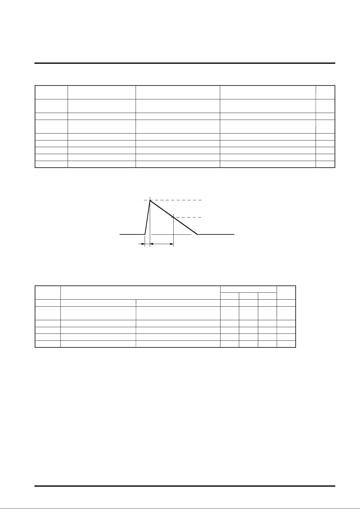
WAVEFORM DIAGRAM
ABNORMAL VOLTAGE DETECTION FUNCTION
Normally VIBL, fixed amplitude AC supply that has been rectified
and divided by a resistor, is input to abnormal voltage input IBL.
When a fault occurs in the neutral line N, successive peaks of VIBL
become alternately small and large, with the levels determined by
the load on the AC power lines A and B.
When the amplitude of VIBL exceeds the abnormal voltage trip
voltage VBLT, capacitor CWF connected to pin WF discharges. After
the discharge shase is completed, charging begins again.) When
voltage VWF at WF drops below the WF threshold voltage,
capacitor CTD at TD charges, and after delay time tTD, when
voltage VTD at TD reaches the TD threshold voltage, output OUT
turns on, activating the circuit breaker. To avoid misoperation due
to the effect of repeated one-shot noise that brings VIBL above
VBLT, the voltage drops to the initial value only after time tWF.
This abnormal voltage detection circuit is enabled only when an
external resistor RX is connected to pin RX to enable the current
flow.
1) Voltage waveform when earth leakage is detected.
ILK
V
ILK
V
B
V
B
VMM
0
MM
0
OUT
2) Voltage waveform when abnormal voltage is detected.
Nois
e
WF threshold voltage
tWF(55ms)
IBL
WF
TD
VISL
0
VWF
0
0
IMM
3ms
VBTL(3.9V)
VLKT
MM positive direction threshold voltage
tOUT(45ms)
Note: Values in the parentheses are for reference onl
MM negative direction threshold voltage
TD
V
tTD(300ms)
.
TD threshold voltage
OUT
0

MITSUBISHI <CONTROL / DRIVER IC>
)
M54125L/P
EARTH LEAKAGE CURRENT DETECTOR
ELECTRICAL CHARACTERISTICS(VCC = 5V and Ta = -20 – 80°C unless otherwise noted
Symbol Test conditions
S1
I
S2 Supply current 2
I
VLKT
IMM+
IMM-
tMM
IOU+
IOU-
tOUT
VSM
IS3
Supply current 1
Trip voltage
Sink current
Source current
Detect inhibit time
Sink current
Source current
Output pulse width
Maximum current
voltage
Supply current 3
Parameter
Pin VS
Pin VS
Pin ILK
and VB
Pin MM
Pin MM
Pin MM
Pin OUT
Pin OUT
Pin OUT
Pin VS
Pin VS
VS = 12V, ∆VILK = 0mV, Out : “OFF”
S = 16V, ∆VILK = -15mV, Out : “ON”
V
V
S = 16V, VLKT : 60Hz
Test circuit 3
S = 16V, ∆VILK = 0mV, VMM = 0.8V
V
V
S = 16V, ∆VILK = -15mV, VMM = 0.8V
V
S = 16V
V
S = 16V, ∆VILK = 0mV, VOUT = 0.2V
VS = 16V, ∆VILK = -15mV
VOUT = 0.8V
V
S = 16V
S = 3.5mA
I
V
S = 12V, VILK : 0mV
VIBL = 0V, OUT : “OFF”
Test circuit 2
VS = 12V, VILK : -15mV
IS4
Supply current 4
Pin VS
VIBL = 12V, OUT : “ON”
Test circuit 2
VBLT
IIBL
IWF+
IWF-
tWF
ITD+
ITD-
tDT
Trip voltage
Input current
Sink current
Source current
Recovery time
Sink current
Source current
Delay time
Pin IBL
Pin IBL
Pin WF
Pin WF
Pin WF
Pin TD
Pin TD
Pin TD
VS = 16V
V
S = 16V, VIBL = 4.5V
Test circuit 7
S = 16V, VIBL = 4.5V, VWF = 0.5V
V
VS = 16V, VIBL = 0V, VWF = 0.5V
VS = 16V
VS = 16V, VIBL = 0V, VTD = 0.5V
V
S = 16V, VIBL = 4.5V, VTD = 0.5V
V
S = 16V
Temperature
25
25
-20
25
80
25
25
25
25
25
25
Limits
Min. Max.
4
170
-110
1.7
150
-200
-100
-70
25
20
3.6
1
-22
35
1
-22
200
0.7
1.2
9
370
-250
4
100
26
1
1.4
4.1
0.8
-30
70
-30
420
Unit
mA
mA
mVrms
µA
µA
ms
µA
µA
ms
V
mA
mA
V
µA
mA
µA
ms
mA
µA
ms
Test
circuit
1
1
4
4
10
5
5
10
6
7
8
8
11
9
9
12
APPLICATION EXAMPLE
RX
VS
current
Voltage
regulator
VCC
ILK
MZ Core Series by Soryo Denshi Kagaku Co., Ltd (Mitsubishi Subsidiary)
Note 2 :
RX
Bias
source
VBLT
VB A • VLKT
A
VB
Comparator
M54125L/P
Amplifier
Note 2
ZCT
CWF CTD
IBL WF
Waveform
regulator
Comparator
One-shot
multivibrator
MM
Tel. +81-427-74-7813
CMM
OUT
Delay
circuit
Output
circuit
TD
GND
AC power input
AN
ANB
Load
B

MITSUBISHI <CONTROL / DRIVER IC>
)
q
EARTH LEAKAGE CURRENT DETECTOR
TEST CIRCUIT(CMM = 0.22µF, CTD = 6.8µF and RX = 27kΩ unless otherwise noted
M54125L/P
1
IS 1 and IS 2 Measurement
∆VILK
ILK
VB
VOUT
CMM
MM
OUT
GND
MD234 or
uivalent
E
∗: IS 2 is the value after OUT turns on. (V
3
VLKT
VIBL
ILK
VB
CMM
MM
OUT
VOUT
GND
VS
RX
IBL
WF
TD
out > 0.5V)
VS
RX
IBL
WF
TD
VS
A
IS 1, IS 2
VS
2
IS 3 and IS 4 Measurement
∆VILK
VOUT
CMM
ILK
VB
MM
OUT
GND
VS
RX
IBL
WF
TD
∗: IS 4 is the value after OUT turns on.
4
IMM+ and IMM- Measurement
∆VILK
ILK
VB
A
IMM+
IMM-
VMM
MM
OUT
GND
VS
RX
IBL
WF
TD
RX
CWF
CTD
VS
A
IS 3, IS 4
VIBL
VS
∗:VLKT is the value of VIBL when OUT turns on as VIBL is
gradually increased.
5
IOU+, IOU- Measurement
VS
∆VILK
ILK
VB
CMM
IOU+
A
IOU-
VOUT
MM
OUT
GND
VS
RX
IBL
WF
TD
6
VSM Measurement
ILK
VB
MM
OUT
GND
VS
RX
IBL
WF
TD
VSM
+
V
-
IS

MITSUBISHI <CONTROL / DRIVER IC>
M54125L/P
EARTH LEAKAGE CURRENT DETECTOR
7
VBLT,IIBL Measurement
ILK
VB
MM
OUT
GND
∗: V
BLT is the value of VIBL when VF = 0.5V.
9
ITD+, ITD- Measurement
ILK
VB
MM
OUT
GND
VS
RX
IBL
WF
TD
VS
RX
IBL
WF
TD
RX
RX
ITD+
A
ITD-
VS
8
IWF+, IWF- Measurement
VS
ILK
I
IBL
A
+
V
VWF
-
VIBL
10
VS
IBL
V
VTD
VB
MM
OUT
GND
tMM,tOUT Measurement
VILK
VOUT
VILK
VOUT
tMM
CMM
VS
RX
IBL
WF
TD
ILK
VB
MM
OUT
GND
10ms
RX
t
OUT
1.4V
VS
RX
IBL
WF
TD
IWF+
IWF-
A
VWF
VS
VIBL
1.8V
0.5V
11
tWF Measurement
VIBL
V
12
VS
ILK
VB
MM
OUT
GND
TD
RX
IBL
WF
4.5V
VS
TD
tWF
RX
CµF
0.5V
3kΩ
0.5V
VIBL
V
0V
TD
tTD Measurement
VOUT
VIBL
OUT
V
ILK
VB
MM
OUT
GND
VS
RX
IBL
WF
TD
0V
tTD
RX
CµF
CTD
0.5V
VS
V
IBL
4.5V
 Loading...