

MITSUBISHI ICs(AV COMMON)
MITSUBISHI
M52959FP
FEATURES
APPLICATION
RECOMMENDED OPERATING CONDITION
Sensor for short distance etc
Rated suooly voltage • • • • • • • • • • • • • • • • 3.0V
Zone data after doing calculation of I1/(I1+I2).
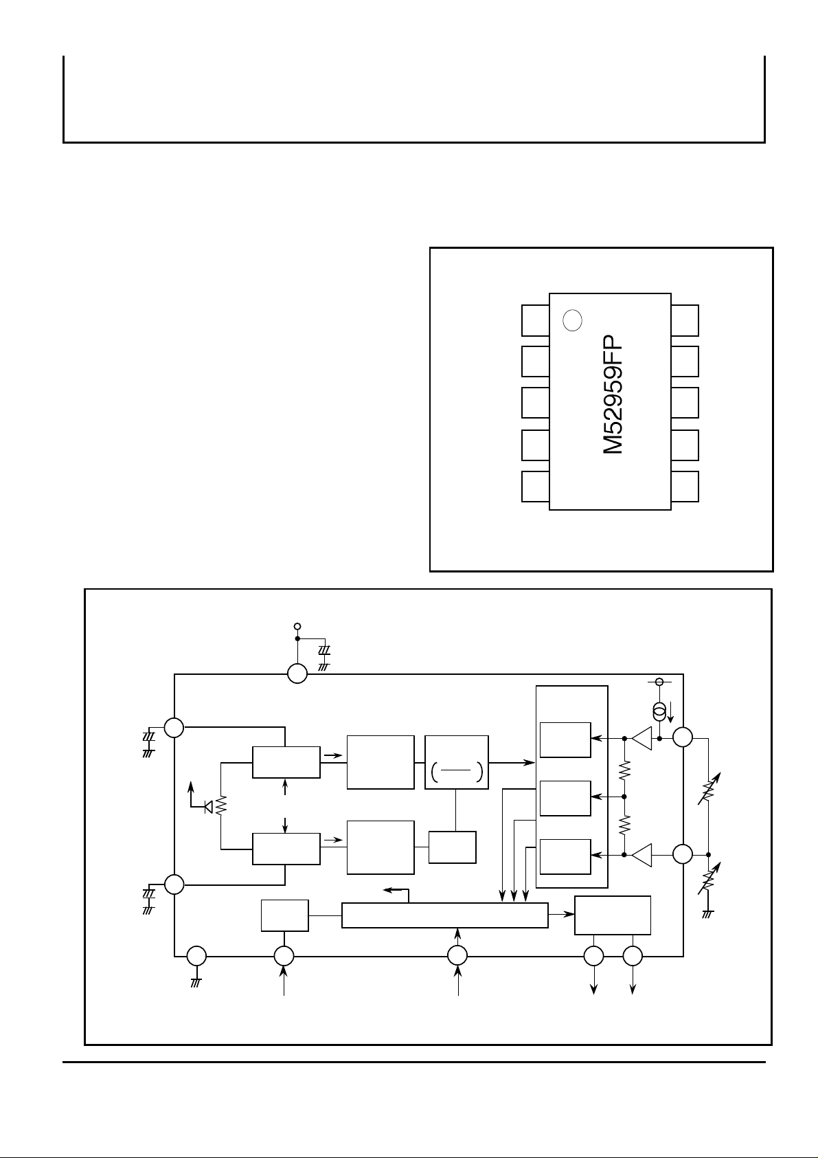
PIN CONFIGURATION (TOP VIEW)
DIAGRAM
GND
CHN
Surround light
rejection
I / V
Transform
Amp
CHF
Cequence Control Logic
Clamp
Circuit
Vcc
HOLD
HOLD
HOLDI1I 2
Reset
Vcc
STB
CONT
OUT1
CV
1.0µF
1.0µF
Calculation
I 1
I 1+I 2
parallel Output
Control Signal Input
Standby Control
Circuit
VR1
VR2
OUT2
9654321
10KΩVR10KΩ
VR
10µA
Buffer
Buffer
Surround light
rejection
I / V
Transform
Amp
Zone
1 2
Level
Zone
2 3
Level
Zone
3 4
Level
PSD ON CHIP DISTANCE DETECTION SIGNAL PROCESSOR
DESCRIPTION
M52959FP is a semiconductor integrated circuit built-in PSD(Position Sensitive Device) and distance detection
signal processor for 3V supply voltage.
This device transforms each signal current(I1 and I2) from PSD sensor to the voltage, and outputs it as the 4
• PSD on chip (Sensor size=0.5mm x 0.7mm)
• Wide operating supply voltage range Vcc=2.0V to 5.5V
• Built-in clamp circuit
VR2
CHN
1
10
Auto focus control for the CAMERA
Supply voltage • • • • • • • • • • • • • • • • 2.0 to 5.5V
BLOCK
7
10
VR1
OUT2
OUT1
CONT
2
3
4
5
9
GND
8
CHF
7
Vcc
STB
6
10Pin Clear Plastic Mold Package (10C2F) or
10Pin Infrared Permeation Plastic Mold Package (10B2F)
Zone
Judgment
>––
Surround light
Hold Capacitor
PSD
(Sensor size
=0.5mm x 0.7mm)
8
Power On
Surround light
Hold Capacitor
( 1 / 8 )
Zone Control
>
––
>
––
Resistance1
Zone Control
Resistance2
Output
Driver
MITSUBISHI
M52959FP
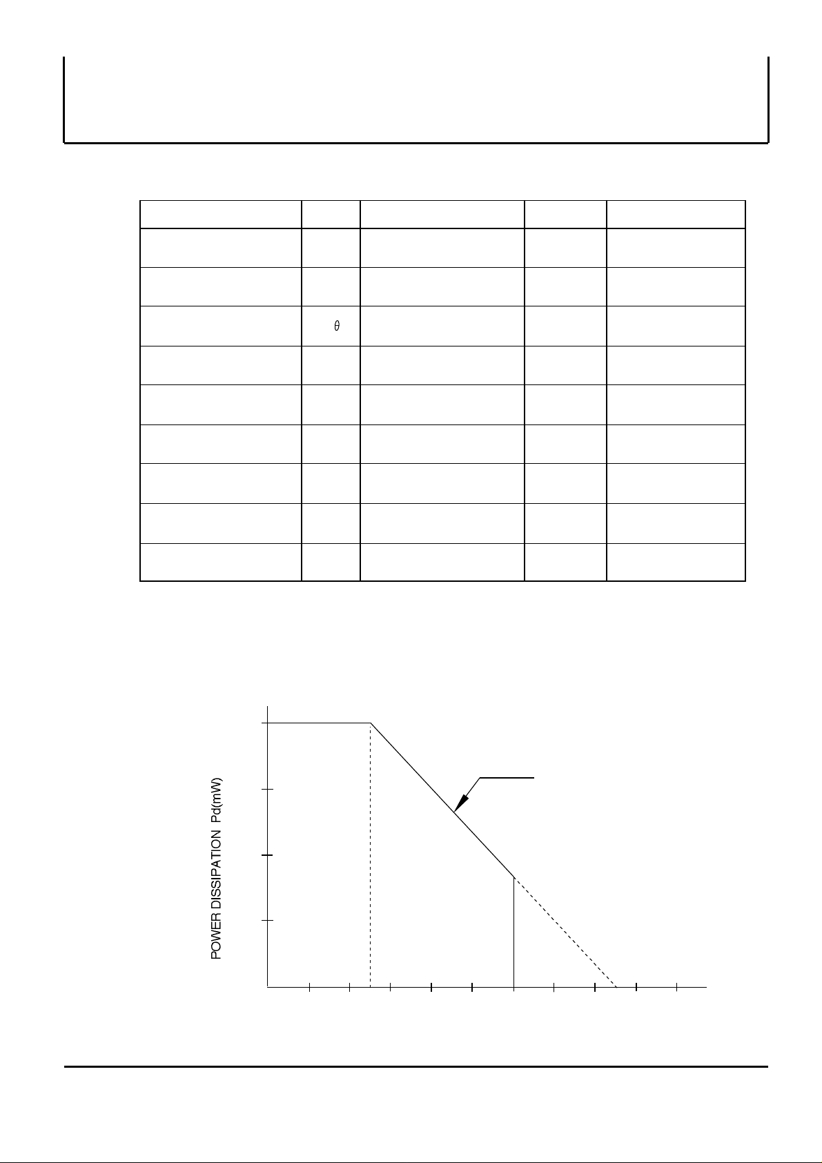
THERMAL DERATING (MAXIMUM RATING)
ABSOLUTE MAXIMUM RATINGS
Parameter
Supply voltage
Power dissipation
Operating temperature
Storage temperature
Thermal derating
Symbol
VccPdTopr
TstgKRatings
7.0
200
- 30 to 85
UnitVmW˚CmW/˚C
3.3
Pin input voltage
V
Output pin inflow current
Isout
0.5mA- 10 to 60
˚C
Remark
note 1
Ta ≥ 25˚C
Pin3,4,5,6
note 2
NPN open collector
note 2 : As a principle,do not provide over supply voltage or under ground voltage.
Ta = 25˚C
Surge voltage
Vsurge
1000V over
R=1.5KΩ
MITSUBISHI ICs(AV COMMON)
PSD ON CHIP DISTANCE DETECTION SIGNAL PROCESSOR
(Ta=25˚C ,unless noted)
VIF
Another pin input voltage
note 1 : As a principle,do not provide a supply voltage reversely.
200
VI/O - 0.3 to Vcc+0.3 V
7.0
+
_
C=100PF
150
100
50
0
10 20 30 40 50 60 70 80 90 100
25 85
AMBIENT TEMPERATURE Ta (˚C)
( 2 / 8 )
- 3.3mW/˚C
MITSUBISHI
M52959FP
PSD ON CHIP DISTANCE DETECTION SIGNAL PROCESSOR
VCC
OUT1
STB
CONT
Surround light Hold
CH Quik Charge
Output signal
IC control content
Power On Reset
Zone Judgment
(Hi Edge)
Output Latch
2
1
CH Quik
Charge
Distance Detection
Controls
100µsec
1.0msec
min
1msec
min
1msec
min
100µsec
min
100µsec
min
100µsec
100µsec
100µsec
Stabilization
Period
OUT2
min
100µsec
min
100µsec
SEQUENTIAL TIME CHART EXAMPLE
Input signal
MITSUBISHI ICs(AV COMMON)
Total Time
25msec
1.0msec
1.2msec
27msec+1.2msec x n
( n : Frequency of Radiation)
1. First,STB terminal set Low,then Power On Reset circuit operate.This Power On Reset circuit resets Built-in logic
circuits.
2. After Power On Reset circuit stoped,Surround light Hold Capacitor quik charge between the first CONT pulse
edge from High to Low and second CONT pulse edge from High to Low.
3. After quik charge,set Stabilization Period for about 1ms.
4. After quik charge,Surround light hold between the first CONT pulse edge from Low to High and second CONT
pulse edge from Low to High.
5, After quik charge,Zone judges at the first CONT pulse edge from High to Low and output the Zone Data to
OUT1,OUT2 terminals by 2bit at next CONT pulse edge from Low to High.
6. It can repeat distance detection by continuing control of 4 and 5.
7. It needs the signal synchronized with timing of Surround light hold as radiation control signal of IRED.
( 3 / 8 )
MITSUBISHI ICs(AV COMMON)
MITSUBISHI
M52959FP
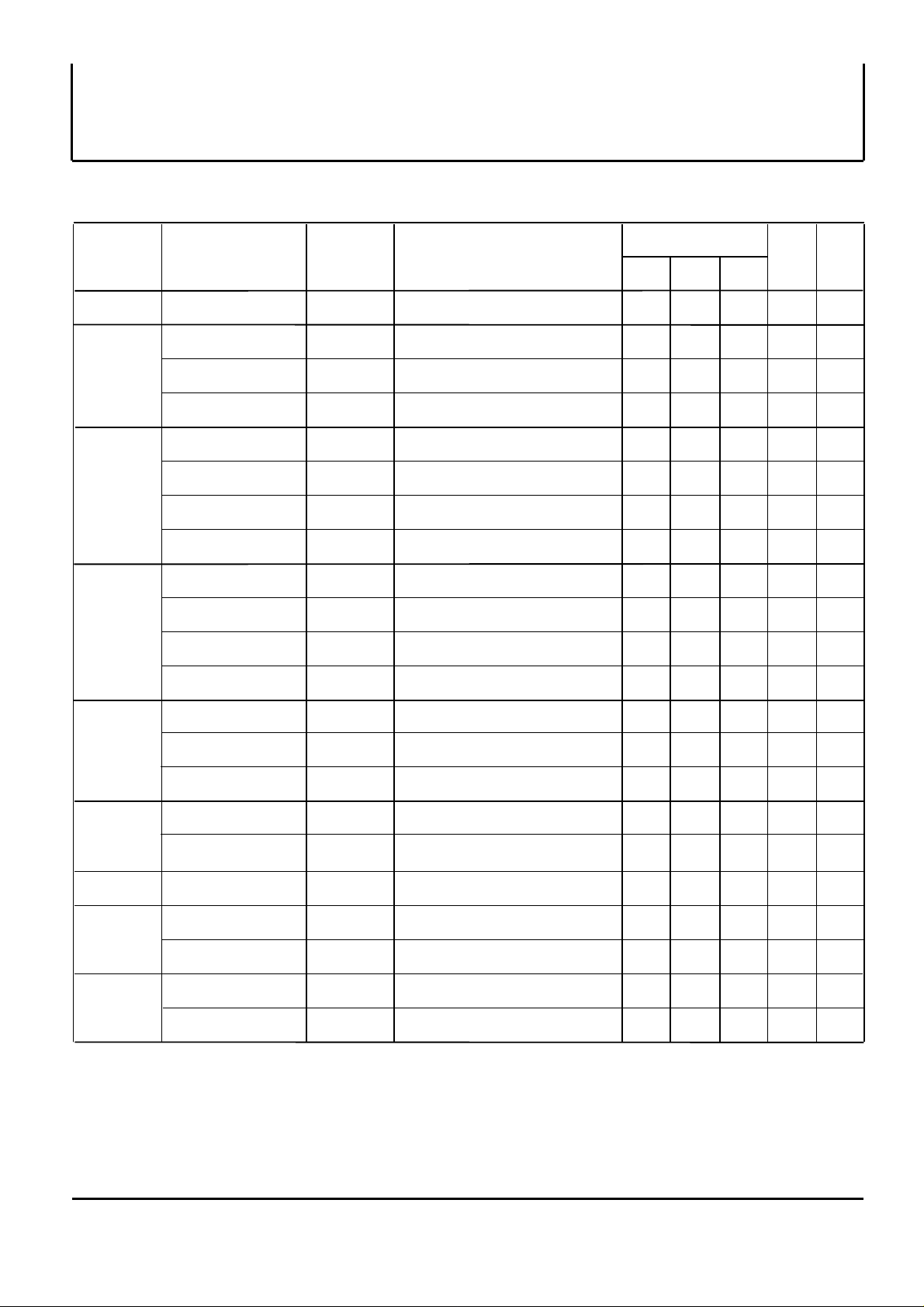
Classfication
Parameter
Symbol
Test condition
Limit
Unit
Note
Min.
Typ.
Max.
Operating supply
voltage range
VCCVUsual consuming current
ICC–mA–mA
While CH Quick charge
cunsuming current
V842.0
3.0
5.5
ICCQC
IOUT
VOUT
ST1–140
196
0.25
*1
While Quick charge
consuming current
*1
VR output current
IVR
VVR=0V
µA
-13-7-10
OUT leak current
OUT saturationt voltage
VIN=5.5V
IOUT=500µA
0.3–––µA
1.0
Far diatance detection
characteristics
Near distance detection
characteristics
ST2
No Signal
Signal = 100nA
Clamp level
PSD resistance value
ICLAM
RPSD
nAKΩ0.5*1*1*2*3*4*4
CONT
terminal
VCOH
VVVIH=5.5V
µAµAVCOL
ICOH
ICOL
VIL=0V
1.1
7.0–0
0.3––
1.0–-78
-42
-60
STB
terminal
VSTH
VSYL
ISTH
ISTL
VIH=5.5V
VIL=0V
VVµA
µA
VCC
-0.3
7.0–––3.0
-150
-50
-100
While STAND BY
consuming current
ICCS*1*1––
1.0µA6.0
8.0
10.0
13.0
Nearest
zone
Farther
zone
0.3
CH Quick charge current
ICHQC
-1200
µA
CH stationary charge
current
ICHC
µA
CH stationary discharge
current
ICHDµAVCH=0V
VCH=1.5V
-800
-400
-30
-20
-10102030*1*1*1
VCH=0V
0.75
0
Consuming
current
Surround
light Hold
Capacitor
Output
circuit
AF
characteristics
CONT "H" input voltage
CONT "L" input voltage
CONT "H" input current
CONT "L" input current
STB "H" input voltage
STB "L" input voltage
STB "H" input current
STB "L" input current
–
PSD ON CHIP DISTANCE DETECTION SIGNAL PROCESSOR
ELECTRICAL CHARACTERISTICS (Ta=25˚C , Vcc=3.0V , dark situation , unless otherwise noted)
( 4 / 8 )
MITSUBISHI ICs(AV COMMON)
MITSUBISHI
M52959FP
IRED
IRED
Radiation
control signal
PSD ON CHIP DISTANCE DETECTION SIGNAL PROCESSOR
*1 Set up the logic control terminal, correspond to the parameter.
*2 This measuring have to put DUT box under dark condition.
*3 Regulate IRED driving current so that PSD output will become equivalent to 100nA and irradiate IC with
synchronizing IRED radiation.
Set zone resistance VR1 = VR2 = 2KΩ
*4 Reference value
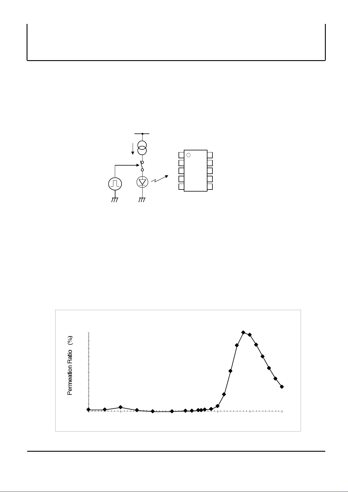
PSD SPECTRAL RESPONSIVITY CHARACTERISTICS
Characteristic at using Infrared Permeation Plastic Mold Package
100
90
80
70
60
50
40
30
20
10
0
400 500 600 700 800 900 1000
Wave length peak 880nm
WAVE LENGTH (nm)
( 5 / 8 )

MITSUBISHI
M52959FP
Interface
Unit
Max.
Typ.
Min.
conditions
and note
VµA0.3
1.0
IOL=500µA
VIN=5.5V
1.1
7.000.3
1.0
-78
-42
-60
VCC
-0.3
7.0
3.0
-150
-50
-100VµA
VIH=5.5V
VIL=0V
VIH=5.5V
VIL=0V
V
µA
CONT
0.3
0
"L" output
current
"H" leak
current
"H" input
voltage
"L" input
voltage
"H" input
current
"L" input
current
"H" input
voltage
"L" input
voltage
"H" input
current
"L" input
current
MITSUBISHI ICs(AV COMMON)
PSD ON CHIP DISTANCE DETECTION SIGNAL PROCESSOR
Ta=25˚C, VCC=3.0V , dark condition
Terminal name
STB
Circuit diagram
Parameter
Limit
Test
OUT
( 6 / 8 )

MITSUBISHI ICs(AV COMMON)
MITSUBISHI
M52959FP
M52959FP Zone adjustment range
input current raio I1 : I2
VR2 adjustment range
VR1 adjustment range
APPLICATION EXAMPLE
and VR2 , the adjustment range becomes the bottom figure.
OUT1
OUT2
Zone 1
Zone 2
Zone 3
Zone 4
near
far
LLHLLHH
H
style from OUT1 and OUT2.
( 7 / 8 )
PSD ON CHIP DISTANCE DETECTION SIGNAL PROCESSOR
ADJUSTMENT RANGE OF ZONE SETTING RESISTANCE AND OUTPUT FUNCTION
In case of using volume 10KΩ for the setting resistance VR1
Zone Decision result is outputted as
mentioned in the bottom figure by the digital
GND
10KΩ VR
10KΩ VR
OUT2
OUT1
CONT
STB
Vcc
VR2
VR1
OUT2
OUT1
CONT
CHN
GND
CHF
Vcc
STB
1.0µF
1.0µF
470µF
10Ω

MITSUBISHI ICs(AV COMMON)
MITSUBISHI
M52959FP
Note regarding these materials
( 8 / 8 )
PSD ON CHIP DISTANCE DETECTION SIGNAL PROCESSOR
• These materials are intended as reference to assist our customers in the selection of the Mitsubishi
semiconductor product best suited to the customer's application; they do not convey any license
under any intellectual property rights, or any other rights, belonging to Mitsubishi Electric
Corporation or a third party.
• Mitsubishi Electric Corporation assumes no responsibility for any damage, or infringement of any
third-party's right,originating in the use of any product data, diagrams, charts of circuit application
examples contained in these materials.
• All information contained in these materials, including product data, diagrams and charts, represent
information on products at the time of publication of these materials, and are subject to change by
Mitsubishi Electric Corporation without notice due to product improvements or other reasons.
It is therefore recommended that customers contact Mitsubishi Electric Corporation or an
authorized Mitsubishi Semiconductor product distributor for the latest product information before
purchasing a product listed herein.
• Mitsubishi Electric Corporation semiconductors are not designed or manufactured for use in a
device or system that is used under circumstances in which human life is potentially at stake.
Please contact Mitsubishi Electric Corporation or an authorized Mitsubishi Semiconductor product
distributor when considering the use of a product contained herein for special applications, such as
apparatus or systems for transportation, vehicular, medical, aerospace, nuclear repeater use.
• The prior written approval of Mitsubishi Electric Corporation is necessary to reprint or reproduce in
whole or in part these materials.
• If these products or technologies are subject to the Japanese export control restrictions, they must
be exported under license from the Japanese government and cannot be imported into a country
other than the approved destination.
Any diversion or reexport contrary to the export control laws and regulations of Japan and/or the
country of destination is prohibited.
• Please contact Mitsubishi Electric Corporation or an authorized Mitsubishi Semiconductor product
distributor for further details on these materials or the products contained therein.
 Loading...