Outline 16P2E-A
16
13
14
15
1
4
3
2
12
5
11
6
7
8
10
9
M52957FP
PSDN
CHN
V
CC
(TESTN)
NC
STB
CINT
RESET
SOUT
PSDF
CHF
GND1
(TESTF)
NC
GND2
CLALV
HOLD
INT
MITSUBISHI ICs (AV COMMON)
M52957FP
DISTANCE DETECTION SIGNAL PROCESSING FOR 3V SUPPLY VOLTAGE
DESCRIPTION
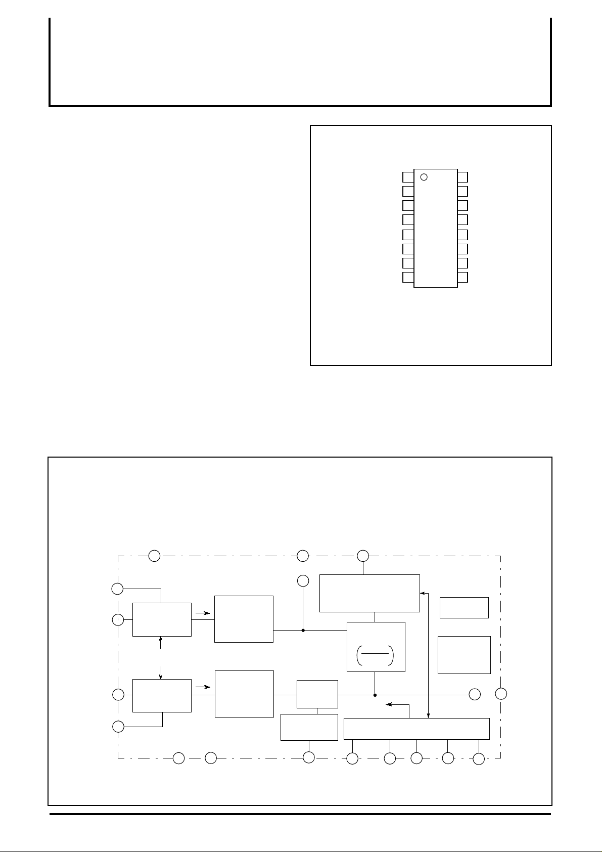
M52957FP is a semiconductor integrated circuit containing
distance detection signal processing circuit for 3V supply voltage.
This device transforms each optical inflow current I1 and I2 from
PSD SENSOR into the voltage, and integrates that output after
doing calculation corresponds to I1/(I1+I2), and outputs it as the
time data(pulse term).
FEATURES
Wide supply voltage range Vcc=2.2 to 5.5V
•
Includes clamp level switching circuit
•
(Switch is 16 kinds by outside control)
Includes standby function
•
Includes power on RESET function
•
APPLICATION
Auto focus control for the CAMERA
Sensor for short distance etc
RECOMMENDED OPERATING CONDITION
Supply voltage range......................................................2.2 to 5.5V
Rated supply voltage.................................................................3.0V
PIN CONFIGURATION
(TOP VIEW)
NC:NO CONNECTION
BLOCK DIAGRAM
CHN
2
1
PSDN
PSDF
CHF
16
15
VCC
3 4
TESTN
1
STATIONARY
LIGHT
REMOVE
HOLD
HOLD
STATIONARY
LIGHT
REMOVE
14
GND1
I
I2
12
GND2
I/V
TRANSFORM
AMP
I/V
TRANSFORM
AMP
Note: pin4,13 is connected only engineering sample
NC
CLANP
CIRCUIT
CLAMP LEVEL
SWITCHING
11
CLALV STB RESET INT HOLD SOUT
CINT
6
PULSE WIDTH
TRANSFORM
(DOUBLE INTEGRATION)
RECKON
I1
I1+I2
HOLD
SEQUENTIAL CONTROL LOGIC
5
7
9
BIAS
REFERENCE
VOLTAGE
10
TESTF
13
NC
8
1

≥
±
MITSUBISHI ICs (AV COMMON)
M52957FP
DISTANCE DETECTION SIGNAL PROCESSING FOR 3V SUPPLY VOLTAGE
ABSOLUTE MAXIMUM RATINGS
(Ta=25˚C,unless otherwise noted)
Symbol Parameter Ratings Unit Remark
V
CC
Supply voltage 7.0 V note 1
Pd Power dissipation 320 mW Ta=25˚C
K
V
IF
V
I/O
I
sout
T
opr
T
stg
surge
V
Note 1. As a principle,do not provide a supply voltage reversely.
2. As a principle,do not provide the terminals with the voltage over supply voltage or under ground voltage.
ELECTRICAL CHARACTERISTICS
Thermal derating -3.2 mW/ ˚C
Ta 25˚C
Pin supply voltage 7.0 V Pin5,7,8,9,10,11
Another pin supply voltage -0.3 to V
+0.3 V note 2
CC
Output pin inflow current 0.5 mA NPN open collector
Operating temperature -10 to 50 ˚C
Storage temperature -40 to 125 ˚C
Surge voltage
200V over
C=200PF
R=0 Ω
(Ta=25˚C,Vcc=3.0V, unless otherwise noted)
Symbol Classification Parameter Test conditions
CC
V
CC1
I
CC2
I
CC3
I
CC4
I
V
HOH
V
HOL
I
HOH
I
HOL
V
INH
V
INL
I
INH
I
INL
V
CLH
V
CLL
I
CLH
I
CLL
V
REH
V
REL
I
REH
I
REL
V
STH
STL
V
STH
I
STL
I
CHQC
I
CHC
I
CHD
I
Consuming
current
HOLD pin
INT pin
CLALV pin
RESET pin
STB pin
HOLD C
Operating supply
voltage range
Usual consuming current - 5.9 7.7 mA
While Rapid charge
consuming current 1
While Rapid charge
consuming current 2
While CH rapid charge
consuming current
While CH and CINT rapid charge
consuming current
While STAND BY consuming current - - 1.0 µ A
HOLD "H" input voltage 1.1 - 7.0 V
HOLD "L" input voltage -0.3 - 0.3 V
HOLD "H" input current V
HOLD "L" input current V
=5.5V - - 1.0 µ A
IH
=0V -100 -75 -50 µ A
IL
INT "H" input voltage 1.1 - 7.0 V
INT "L" input voltage -0.3 - 0.3
INT "H" input current V
INT "L" input current V
=5.5V - - 1.0 µ A
IH
=0V -100 -75 -50 µ A
IL
CLALV "H" input voltage 1.1 - 7.0 V
CLALV "L" input voltage -0.3 - 0.3 V
CLALV "H" input current V
CLALV "L" input current V
=5.5V - - 1.0 µ A
IH
=0V -100 -75 -50 µ A
IL
RESET "H" input voltage 1.1 - 7.0 V
RESET "L" input voltage -0.3 - 0.3
RESET "H" input current V
RESET "L" input current V
=5.5V - - 1.0 µ A
IH
=0V -100 -75 -50 µ A
IL
STB "H" input voltage
STB "L" input voltage -0.3 - 0.3 V
STB "H" input current V
STB "L" input current V
CH rapid charge current IPSD=5 µ A,
CH stationary charge current
CH stationary discharge current V
IH
=5.5V - - 3.0 µ A
IL
=0V -150 -100 -50 µ A
CH
V
=0V -2000 -1000 -500 µ A
CH
V
=0V -30 -20 -10 µ A
CH
=1.5V 10 20 30 µ A
Limits
Min. Typ. Max.
2.2 3.0 5.5 V
- 17.7 23.0 mA
- 19.0 24.7 mA
V
CC
-0.3
- 7.0 V
Unit
V
V
2

∆
µ
MITSUBISHI ICs (AV COMMON)
M52957FP
DISTANCE DETECTION SIGNAL PROCESSING FOR 3V SUPPLY VOLTAGE
∆
∆
∆
∆
∆
∆
∆
∆
ELECTRICAL CHARACTERISTICS
Symbol Classification Parameter Test conditions
I
CINTC
V
CINT
I
CI1
CI2
I
∆
I
CI1
I
CI2
∆
CI12
I
(9:1)-1
D
D
(6:4)-1
(3:7)-1
D
AF-1 AF slope -1 6.57 8.89 11.21 msec
Double
integration
AF input
condition 1
CINT rapid charge current V
CINT reference voltage GND criterion 1.6 1.8 2.0 V
The first integration current
The second integration current -3.31 -2.54 -1.77 µ A
The first integration
current stability percentage
The second integration
current stability percentage
The first and second
integration current ratio
AF output time(9:1)-1 Near side 9 : Far side 1 11.78 13.40 15.02 msec
AF output time(6:4)-1 Near side 6 : Far side 4 7.77 8.95 10.13 msec
AF output time(3:7)-1 Near side 3 : Far side 7 3.77 4.51 5.25 msec
(cont.)
Limits
Min. Typ. Max.
=1V(CINT stable period) 84 120 156 µ A
CI
V
V
I
CI1
CINT
CHF
=1.5V
=2V, V
/ I
CI2
CHN
=0V
4.2 6.0 7.8
- - 10 %
- - 10 %
2.12 2.36 2.60
LAF-1 AF linearity-1 0.9 1.0 1.1
(9:1)-2
D
D
(6:4)-2
(3:7)-2
D
AF-2 AF slope -2 6.57 8.89 11.21 msec
AF input
condition 2
AF output time(9:1)-2 Near side 9 : Far side1 11.78 13.40 15.02 msec
AF output time(6:4)-2 Near side 6 : Far side4 7.77 8.95 10.13 msec
AF output time(3:7)-2 Near side 3 : Far side7 3.77 4.51 5.25 msec
LAF-2 AF linearity-2 0.9 1.0 1.1
(9:1)-3
D
D
(6:4)-3
(3:7)-3
D
AF-3 AF slope -3 6.57 8.89 11.21 msec
AF input
condition 3
AF output time(9:1)-3 Near side 9 : Far side1 11.78 13.40 15.02 msec
AF output time(6:4)-3 Near side 6 : Far side 4 7.77 8.95 10.13 msec
AF output time(3:7)-3 Near side 3 : Far side 7 3.77 4.51 5.25 msec
LAF-3 AF linearity-3 0.9 1.0 1.1
D
(9:1)
AF output time(9:1)
AF input
condition
(6:4)
D
AF output time(6:4)
1 minus 2
(3:7)
D
SOUTL
I
VSOUTS SOUT saturation voltage IOUT=500µA - - 0.3 V
∆INF
IPSD Stationary light remove current - - 30 µA
CLAM
I
Data
Sensor
AF output time(3:7)
SOUT leak current V
Signal light saturation current 3.0 - - µA
Clamp level Change quantity for Typ.
Near side 9 : Far side1
(Consition 1-2)
Near side 6 : Far side4
(Consition 1-2)
Near side 3 : Far side7
(Consition 1-2)
IN
=5.5V - - 1.0 µA
current
- - 280 µ sec
- - 280 µ sec
- - 280 µ sec
-30 - 30 %
Unit
A
3
 Loading...