Mitsubishi M52757FP Datasheet

MITSUBISHI ICs (Monitor)
M52757FP
B
R
G
Vcc(5V)
WIDE BAND ANALOG SWITCH
DESCRIPTION
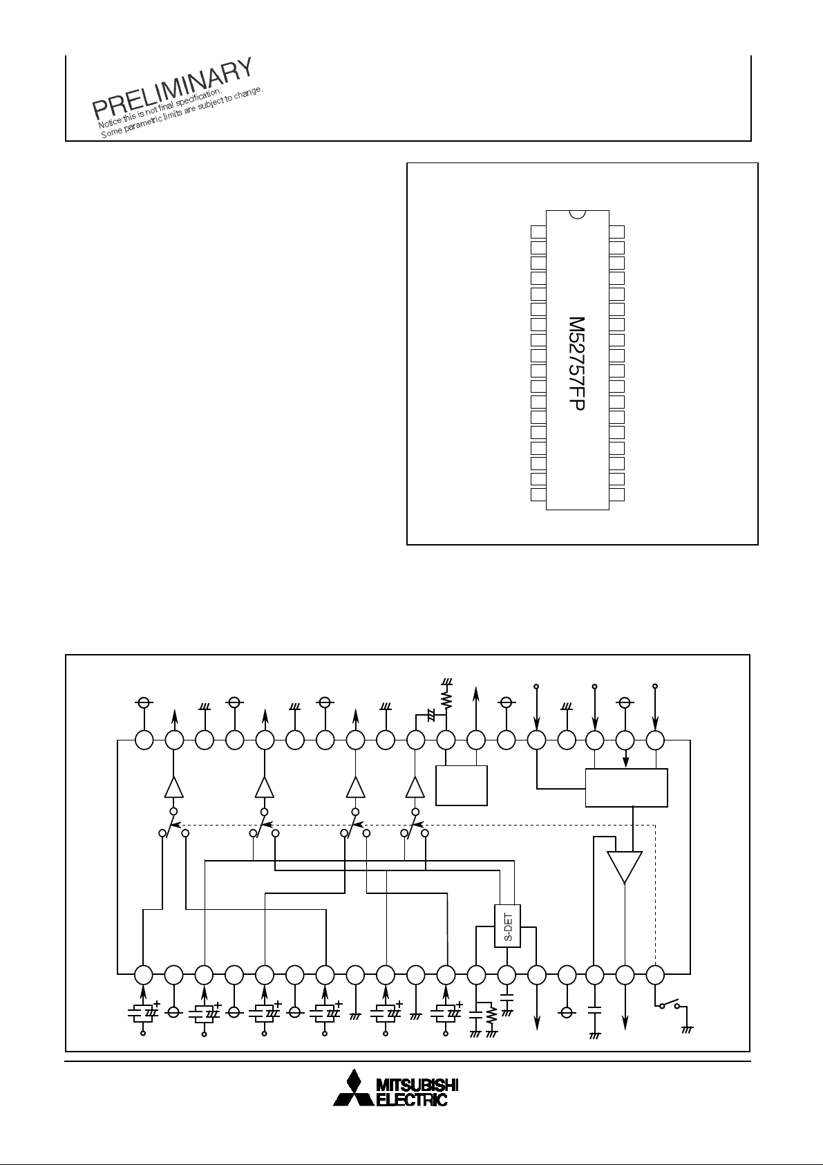
The M52757FP is a semiconductor integrated circuit for
the RGB interface. The device features switching signals
input from two types of image sources and outputting the
signals to the CRT display,etc. The frequency band of
video signals is 250MHz, acquiring high-resolution
images, and are optimum as an interface IC with highresolution CRT display and various new media.
It includes Sync-separator, Video-signal-detector, and
Sync-on G detector (SOG-DET.).
FEATURES
• Frequency band width : R.G.B ...................250MHz
• Input level : R.G.B...............................0.7Vp-p (Typ.)
• Video signal-detector
Responsive frequency............................... ~50MHz
Input level............................................0.7Vpp (Typ.)
Detected level......................................150mV (Typ.)
(Measure bottom to DET.level)
• Only the G channel is proveded with buffer video output.
• It is possible to save the consumption current by
stopping current supply to Pin 2,4,6,20,24,30,33,35
because SOG-DET can be operated with only Vcc5
(Pin 15) as power save mode.
• Include Sync Separation,Video signal detector, and
Sync-on G detector.
APPLICATION
Display monitor
PIN CONFIGURATION (TOP VIEW)
Input1 (R)
Vcc1 (R)
Input1 (G)
Vcc1 (G)
Input1 (B)
Vcc1 (B)
Input2 (R)
GND1
Input2(G)
GND5
Input2 (B)
SyncDET1
SyncDET2
S-DETout
Vcc5
VideoDET-Hold
V-DETout
SWITCH
1
2
3
4
5
6
7
8
9
10 27
11 26
12
13
14 23
15
16 21
17
18
36
VCC2 (R)
35
OUTPUT (R)
34
GND2(R)
33
Vcc2(G)
32
OUTPUT(G)
31
GND2 (G)
30
Vcc2 (B)
29
OUTPUT(B)
28
CND2(B)
G Buffer out
Sync SEP in
25
Sync SEP out
24
Vcc3
V-DET in3
22
GND4
V-DET in2
20
Vcc4
19
V-DET in1
Outline: 36P2R-D
RECOMMENDED OPERATING CONDITION
Suply voltage range 4.75~5.5V
Rated voltage 5.0V
BLOCK DIAGRAM
Vcc2(R)
OUTPUT(R)
36
35
2 3 4
1
INPUT1(R) INPUT1(G) INPUT1(B)
Sync SEP in
26
Sync SEP out
25
Vcc2(G) Vcc2(B)
OUTPUT(G) OUTPUT(B)
323334
31
30 29 28 27
G Buffer out
(for Sync on G)
Sync
G
5 6 7 8 9 10 11 12 13 14 15
Vcc1(G)Vcc1(R)
Vcc1(B)
INPUT2(R) INPUT2(G)
sepa
INPUT2(B)
SyncDET1
Vcc3
24
SyncDET2
23
S-DET
OUT
22
POWER
SAVE
Vcc5
VideoDET-Hold
V-DET in 2V-DET in 3
Vcc4
21 20 19
OR
16
17
V-DET out
V-DET in 1
18
SW GND : INPUT1
SW OPEN : INPUT2
( / 5 )
1

M52757FP
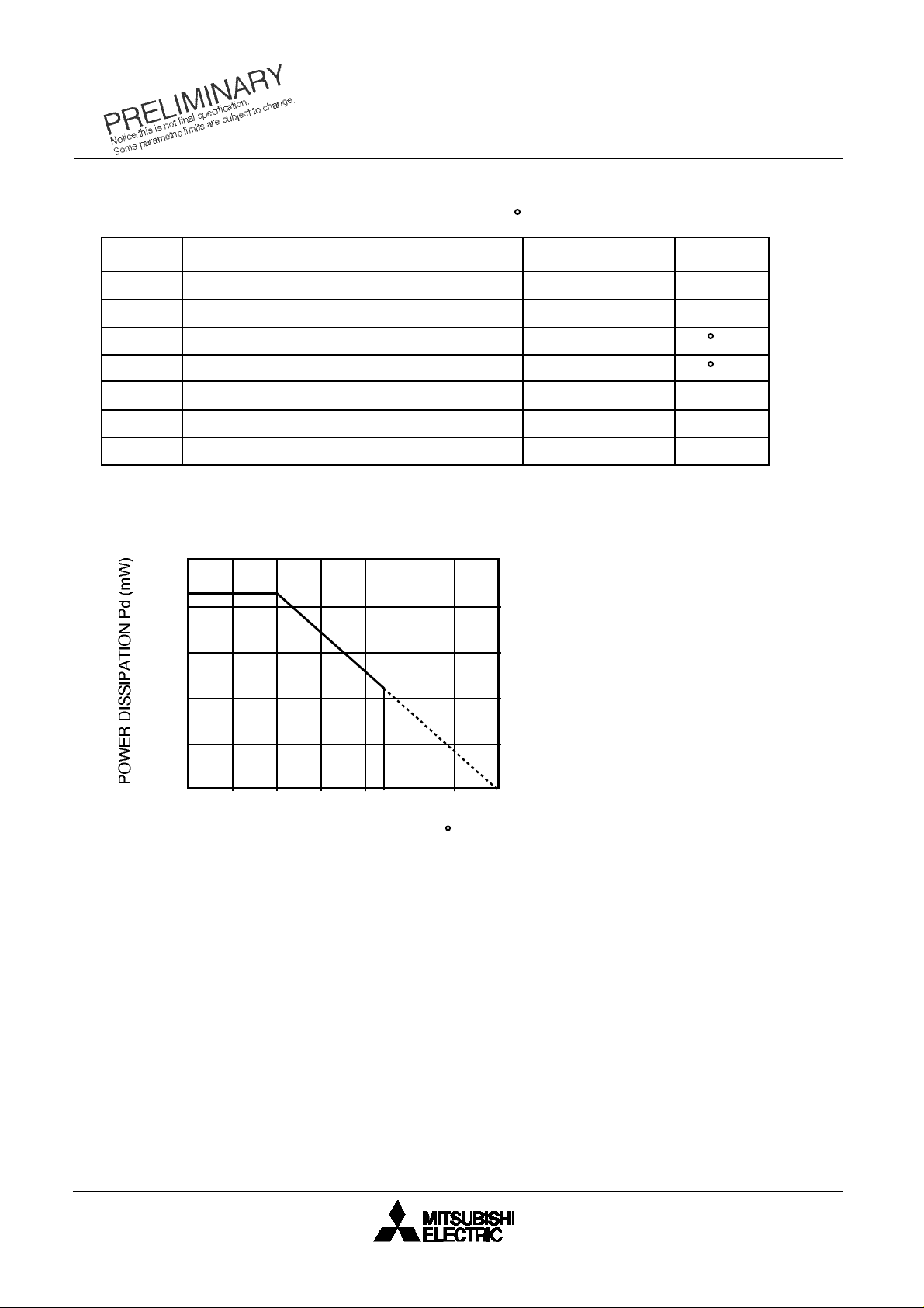
ABSOLUTE MAXIMUM RATINGS (Ta=25 C)
MITSUBISHI ICs (Monitor)
WIDE BAND ANALOG SWITCH
Symbol Ratings
Vcc
Pd
Topr
Tstg
Vopr
Vopr'
Sarge
Supply voltege
Power dissiption
Operating temperature
Storage temperature
Recommended operating supply voltege
Recommended operating supply voltege range
Electrostatic discharge
Parameter
7.0
1068
-20~+85
-40~+150
5.0
4.75~5.5
+
200
-
THERMAL DERATING (MAXIMUM RATING)
1250
1068
1000
750
500
Unit
V
mW
C
C
V
V
V
250
-20 0 25 50 8575 100 125 150
AMBIENT TEMPERATURE Ta ( C )
2
( / 5 )
 Loading...