

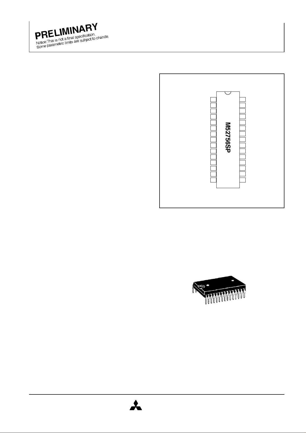
M52756SP
MITSUBISHI ICs (Monitor)
( / 19 )
VCC(H,V,
Buffer,SW,sync Sepa)(5V)
30 pin plastic SDIP
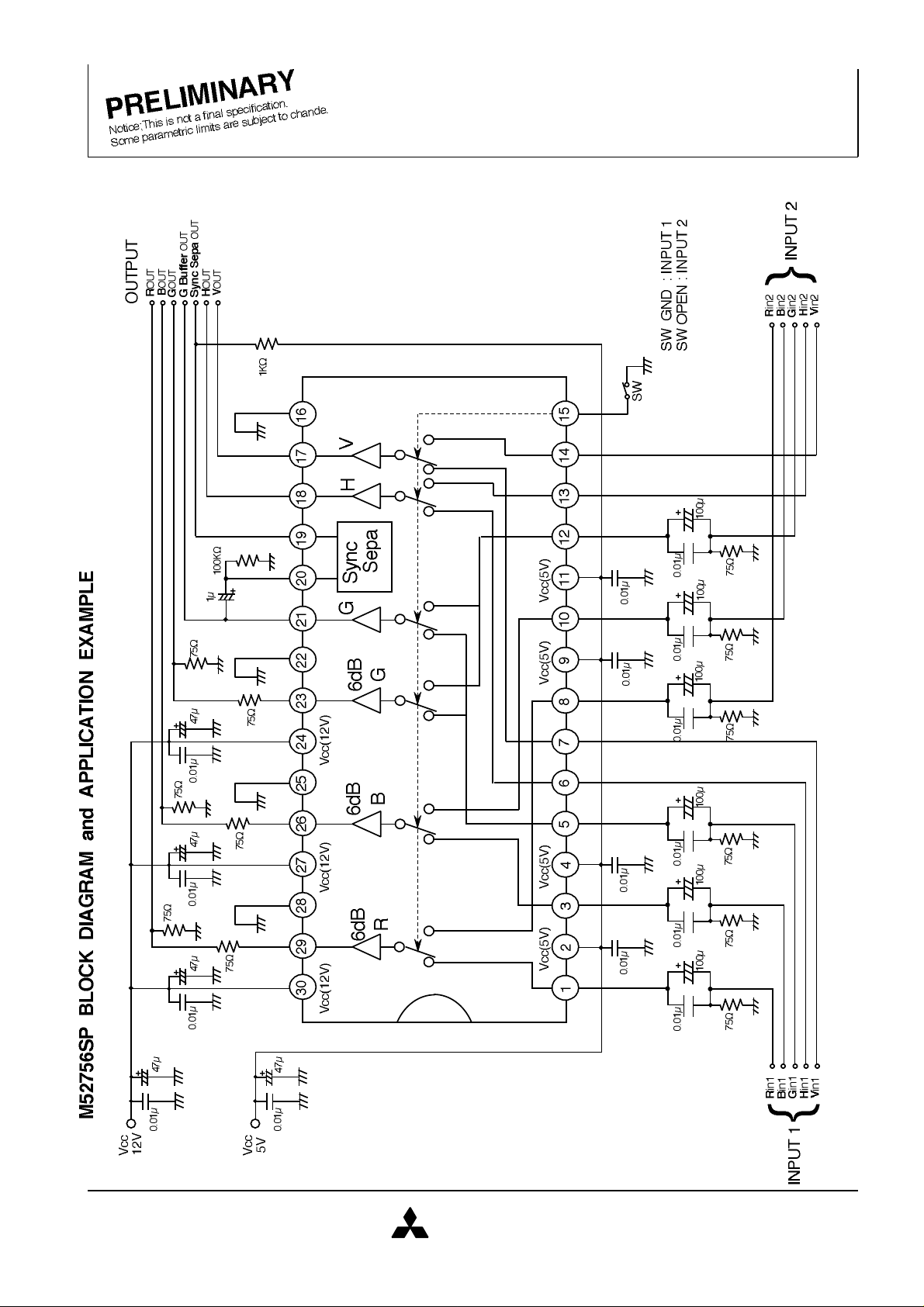
21123456789301029112812271326142517241823222019SWITCH
VCC(R)(12V)
OUTPUT (R)
GND(R)
VCC(B)(12V)
OUTPUT (G)
GND(B)
VCC(G)(12V)
OUTPUT (B)
GND(G)
G Buffer OUT
OUTPUT (H)
OUTPUT (V)
GND(H,V,Buffer,
SW,sync Sepa)
INPUT1 (R)
VCC1(R)(5V)
INPUT1 (G)
INPUT1 (B)
INPUT1 (H)
INPUT1 (V)
INPUT2 (R)
INPUT2 (G)
INPUT2 (B)
INPUT2 (H)
INPUT2 (V)
VCC(G)(5V)
VCC1(B)(5V)
1516Sync Sepa OUT
Sync Sepa IN
WIDE BAND ANALOG SWITCH
DESCRIPTION
The M52756SP is a semiconductor integrated circuit for the
RGBHV interface. The device features switching signals input
from two types of image sources and outputting the signals to
the CRT display, etc. Synchronous signals, meeting a
frequency band of 10kHz to 200kHz, are output at TTL. The
frequency band of video signals is 250MHz, acquiring highresolution images, and are optimum as an interface IC with
high-resolution CRT display and various new media.
DESCRIPTION
• Frequency band: RGB ............................................250MHz
HV...................................10kHz to 200kHz
• Input level: RGB................................................0.7Vp-p(typ.)
HV TTL input....................3.5Vo-p(both channel)
• RGBOUT can drive connected load of 75Ω.
• Only the G channel is provided with sync-on video output.
• The TTL format is adopted for HV output.
• It is possible to save the consumption current by stopping
current supply to Pin 2, 4, 24, 27, 30.
• Sync Separation circuit
PIN CONFIGURATION (TOP VIEW)
Outline 30P4B
APPLICATION
Display monitor
RECOMMENDED OPERATING CONDITION
Supply voltage range.....................4.75 to 5.25V, 11.5 to 12.5V
Rated supply voltage................................................5.0V, 12.0V
MITSUBISHI
ELECTRIC
1
M52756SP
MITSUBISHI ICs (Monitor)
( / 19 )
WIDE BAND ANALOG SWITCH
MITSUBISHI
ELECTRIC
2
M52756SP
( / 19 )
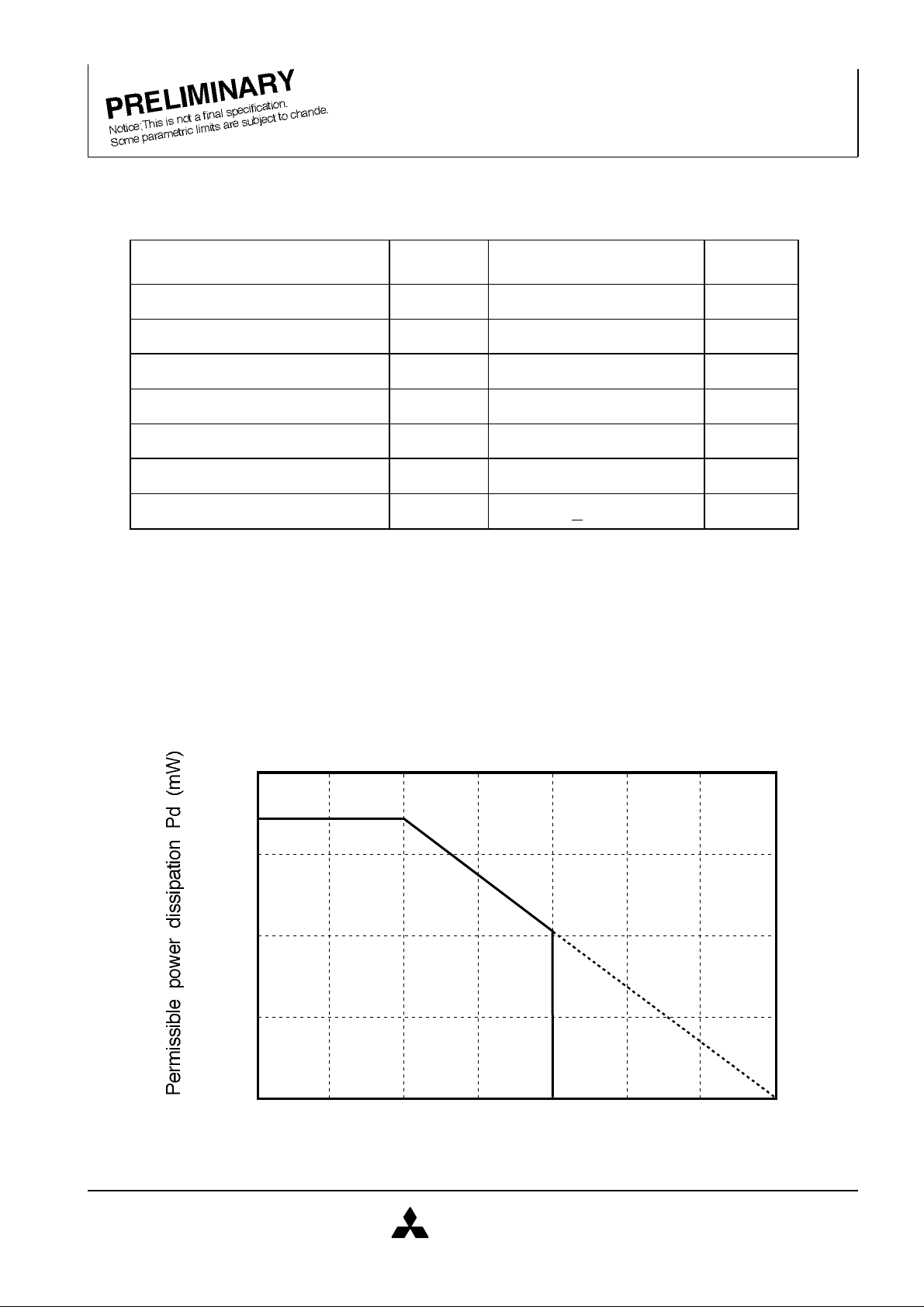
Absolute Maximum Rating
Parameter
Supply voltage
Ambient temperature
Storage temperature
Recommended supply
Recommended sopply
Electrostatic discharge
Power dissipation
Symbol
Vcc
Pd
Topr
Tstg
Vopr
Vopr'
Surge
Rating
Unit
V
mW
˚C˚CVVV
voltage
voltage range
-20~+75
6.0,13.0
1736
-40~+150
5.0,12.0
4.75~5.25,11.5~12.5
Ambient temperature Ta (˚C)
(Ambient temperature: 25˚C)
MITSUBISHI ICs (Monitor)
WIDE BAND ANALOG SWITCH
+150
Thermal Derating Curve
2000
1736
1000
-20
0
25 50 75 100 125 150
MITSUBISHI
ELECTRIC
3
M52756SP
( / 19 )
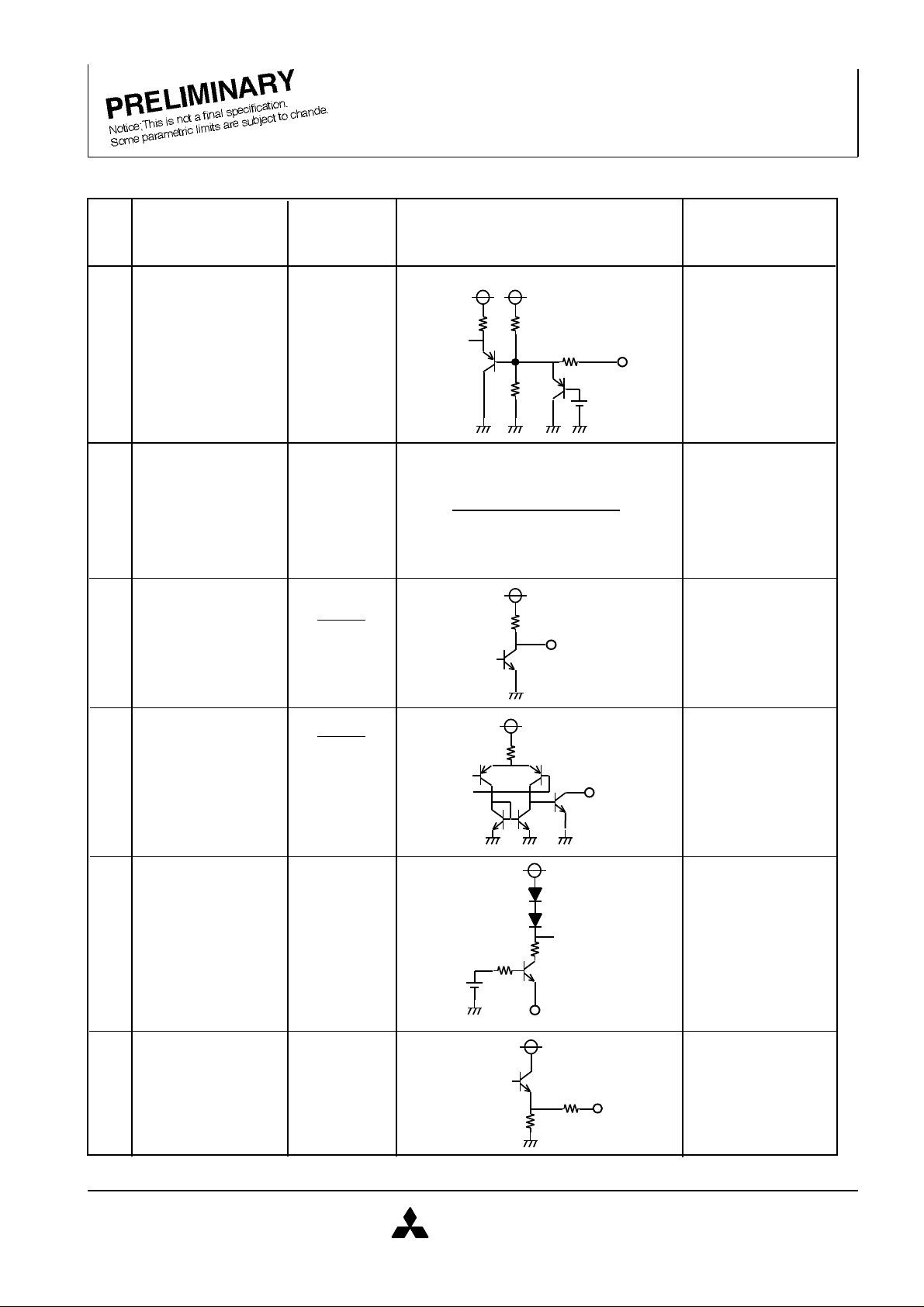
Pin
Description
DC
Voltage[V]
Peripheral circuits at pins
Notes
Pin Description
V
V
2~5V
0~0.8V
No.
MITSUBISHI ICs (Monitor)
WIDE BAND ANALOG SWITCH
1
Input 1 (R)
3
Input 1 (B)
5
Input 1 (G)
2
Vcc(R)
4
Vcc(B)
9
Vcc(G)
11
Vcc(H,V,Buffer,
Input 1 (H)
6
Input 1 (V)
7
SW,SyncSep)
2.25
5.0
3.0V
5.0V
4.5K
750µ
5.0V
20K
Input signal with low
impedance.
Input pulse between
2V and 5V.
2~5V
0~0.8V
10K
10
12
13
14
Input 2 (R)
8
Input 2 (B)
Input 2 (G)
Input 2 (H)
Input 2 (V)
2.25
3.0V
5.0V
4.5K
750µ
5.0V
20K
Input signal with low
impedance.
Input pulse between
2V and 5V.
10K
MITSUBISHI
ELECTRIC
4
M52756SP
MITSUBISHI ICs (Monitor)
( / 19 )
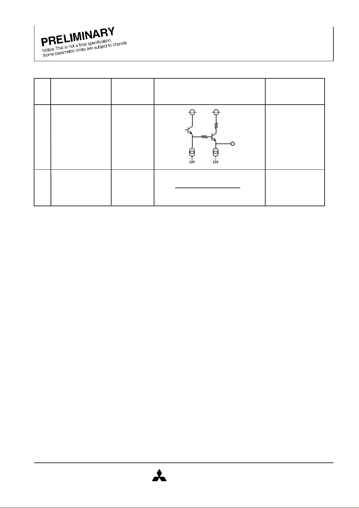
Description
Peripheral circuits at pins
Notes
Pin Description
V
to
OPEN
is
built in.
Connect resistance more
than 1KΩ is necessary
during power supply and
terminal that open
collector output type.
When not used, ground
the pin to GND.
is
built in.
WIDE BAND ANALOG SWITCH
Pin
No.
Voltage[V]
15 Switch 2.4
16
GND(H,V,Buffer,
SW,SyncSep)
22
25
28
17
18
GND(G)
GND(B)
GND(R)
Output(V)
Output(H)
GND
DC
5.0V
10K
13K
12K
5.0V
1K
Switch by OPEN and
GND.
7.3K
2.25V
Output impedance
19
Sync Sepa
OUT
20
Sync Sepa
IN
21
OUTPUT
(G Buffer)
2.3
0.75
5.0V
3.0V
MITSUBISHI
ELECTRIC
1K
500
1K
5.0V
790
5.0V
Input signal with low
impedance.
When not used, set
Output impedance
75
5
M52756SP
MITSUBISHI ICs (Monitor)
( / 19 )
Description
Peripheral circuits at pins
Notes
Pin Description
12.0
WIDE BAND ANALOG SWITCH
Pin
No.
22
OUTPUT(G)
26
OUTPUT(B)
29
OUTPUT(R)
Vcc(G)
24
Vcc(B)
27
Vcc(R)
30
DC
Voltage[V]
1.8
1.6m
75
12.0V
50
8.0m
This output pin can
drive connected load
of 75Ω.
MITSUBISHI
ELECTRIC
6

M52756SP
( / 19 )
Attached Fig.3 Measuring Circuit Diagram
47µ
100µ
75Ω
47µ
a
baSW Aba
SW B
SW 1
b
(Vcc5V)
TP29
TP26
TP23
TP21
TP19
TP18
TP17
TP15
RGB
HVSGSS
SW GND :INPUT1
SW OPEN :INPUT2
1µaSW 2b100µ
75ΩaSW 3ba
SW 4b75ΩaSW 5ba
SW 6ba
SW 7b100µ
75ΩaSW 8ba
SW 9b100µ
75ΩaSW 10ba
SW 11b75ΩaSW 12ba
SW 13ba
SW 14ba
SW 15b47µ
47µ
47µ
75Ω
75ΩaSW 20b100KΩ
1KΩ
baSW B
47µ
baSW B
47µ
75Ω
75Ω
75Ω
75Ω
100µ
0.01µ
0.01µ
0.01µ
0.01µ
0.01µ
0.01µ
0.01µ
0.01µ
0.01µ
0.01µ
0.01µ
0.01µ
0.01µ
0.01µ
0.01µ
0.01µ
0.01µ
100µ
A
MITSUBISHI ICs (Monitor)
WIDE BAND ANALOG SWITCH
B
(Vcc12V)
A A
AA
SG
SG
MITSUBISHI
ELECTRIC
7

M52756SP
MITSUBISHI ICs (Monitor)
( / 19 )
WIDE BAND ANALOG SWITCH
MITSUBISHI
ELECTRIC
8

M52756SP
MITSUBISHI ICs (Monitor)
( / 19 )
WIDE BAND ANALOG SWITCH
MITSUBISHI
ELECTRIC
9

M52756SP
MITSUBISHI ICs (Monitor)
( / 19 )
WIDE BAND ANALOG SWITCH
MITSUBISHI
ELECTRIC
10

M52756SP
MITSUBISHI ICs (Monitor)
( / 19 )
WIDE BAND ANALOG SWITCH
MITSUBISHI
ELECTRIC
11

M52756SP
MITSUBISHI ICs (Monitor)
( / 19 )
WIDE BAND ANALOG SWITCH
MITSUBISHI
ELECTRIC
12

M52756SP
MITSUBISHI ICs (Monitor)
( / 19 )
the
amplitude of input signal when the output waveform is distorted. The amplitude is as Vimax1. And
measure Vimax1 when SG1 as the input signal of Pin 3,Pin 5 in same way.
Next, set SW 15 to OPEN, measure Vimax2 when SG1 as the input signal of Pin8, 10, 12.
note5) 1. The condition is shown as Table 1.
2. Set SW15 to GND, SG2 as the input signal of Pin 1. At this time, read the amplitude output from
T.P 29. The amplitude is as VOR1.
3. Voltage gain Gv1 is
4. The method as same as 2 and 3, measure the voltage gain Gv1 when SG2 as the input signal of
Pin 3, 5.
5. The difference of each channel relative voltage gain is as ∆Gv1.
∆Gv1=Gv1R-Gv1B,Gv1B-Gv1G,Gv1G-Gv1R
6. Set SW15 to OPEN, measure Gv2, ∆Gv2 in the same way.
note5') Voltage gain ∆Gv' is
∆Gv'=Gv1R-Gv2R,Gv1G-Gv2G,Gv1B-Gv2B
note6) 1. The condition is shown as table 1. This test is by active probe.
2. Measure the amplitude output from T.P.21.
3. Measure the GV3,GV4 by the same way as note5.
note7) 1. The condition is shown as table 1. This test is by active probe.
2. Set SW15 to GND, SG2 as the input signal of Pin 1. Measure the amplitude output from T.P.29.
The amplitude is as VOR1.By the same way, measure the output when SG4 is as input signal of
Pin 1, the output is as VOR2.
3. The frequency characteristic Fc1 is
4. The method as same as 2 and 3, measure the frequency Fc1 when input signal to Pin 3, 5.
5. The difference between of each channel frequency characteristic is as ∆Fc1.
6. Set SW15 to OPEN, measure Fc2,∆Fc2.
note8) By the same way as Note7 measure the Fc3, Fc4 when SG5 of input signal.
note9) 1. The condition is shown as Table1. This test is by active prove.
2. Set SW15 to GND, SG3 as the input signal of Pin 1. Measure the amplitude output from T.P.29.
The amplitude is as VOR3.
3. Set SW15 to OPEN, measure the amplitude output from T.P.29. The amplitude is as VOR3'.
4. The crosstalk between two inputs C.T.I.1 is
5. By the same way, measure the crosstalk between two inputs when SG3 as the input
signal of Pin3, Pin 5.
WIDE BAND ANALOG SWITCH
note ) It omits the SW.No accorded with signal input pin because it is already written in Table 1.
SW A is in side a if there is not defined specially.
note1) The condition is shown as Table 1. Set SW15 to GND(or OPEN) and SW A to side b, measure the
current by current meter A(or B). The current is as Icc1(Icc2,Icc3).
note2) Set SW15 to GND (or OPEN), measure the DC voltage of T.P.29(T.P.26,T.P.23) when there is no
signal input.The DC voltage is as VDC1(or VDC2).
note3) Measure the DC voltage of T.P.21 same as note2, the DC voltage is as VDC3(or VDC4).
note4) Set SW15 to GND, SG1 as the input signal of Pin 1.Rising up the amplitude of SG1 slowly, read
GV1= 20 LOG
FC1 = 20 LOG
VOR1 [Vp-p]
0.7 [Vp-p]
VOR2 [Vp-p]
VOR1 [Vp-p]
[dB]
[dB]
C.T.I.1= 20 LOG
MITSUBISHI
ELECTRIC
VOR3' [Vp-p]
VOR3 [Vp-p]
[dB]
13

M52756SP
MITSUBISHI ICs (Monitor)
( / 19 )
input
voltage is as Vith1(Vith 2).
2
2
100%
90%0%10%TrTf
2
2
WIDE BAND ANALOG SWITCH
6. Next, set SW15 to OPEN, SG3 as the input signal of Pin 8, measure the amplitude output
from T.P.29. The amplitude is as VOR4.
7. Set SW15 to GND, measure the amplitude output from T.P.29. The amplitude is as VOR4'.
8. The crosstalk between two inputs C.T.I.2 is
C.T.I.2= 20 LOG
9. By the same way, measure the crosstalk between channels when SG3 as the input signal
of Pin 10,12.
note10) Set SG4 as the input signal, and then the same method as note9, measure C.T.I.3, C.T.I.4.
note11) 1. The condition is as Table 1. This test is by active prove.
2. Set SW15 to GND, SG3 as the input signal of Pin 1. Measure the amplitude output from
T.P.29. The amplitude is as VOR5.
3. Next, measure T.P.26, T.P.23 in the same state, and the amplitude is as VOG 5, VOB 5.
4. The crosstalk between channels C.T.C.1 is
C.T.C1= 20 LOG
5. Measure the crosstalk between channels when SG3 is as the input signal of Pin 3, Pin 5 .
6. Next, set SW15 to OPEN, SG3 as the input signal of Pin8, measure the amplitude output
from T.P.29. The amplitude is as VOR6.
7.Next, measure the amplitude output from T.P.26, T.P.23 in the same state. The amplitude is
as
VOG6, VOB6.
8. The crosstalk between channels C.T.C.2 is
C.T.C2= 20 LOG
VOR4'[Vp-p]
VOR4[Vp-p]
VOG5 or VOB5
VOR5
VOG6 or VOB6
VOR6
[dB]
[dB]
[dB]
9. By the same way, measure the crosstalk between channels when input signal to Pin10, 12.
note12) Set SG4 as the input signal, and the same method as note11, measure C.T.C.3, C.T.C.4.
note13) 1. The condition is as Table 1. Set SW15 to GND (or OPEN).
2. The rising of 10 % ~ 90 % for input pulse is Tri, the falling
of 10 % ~ 90 % for input pulse is Tfi.
3. Next, the rising of 10 % ~ 90 % for output pulse is Tro, the
falling of 10 % ~ 90 % for output pulse is Tfo.
4. The pulse characteristic Tr1, Tf1 ( Tr2, Tf2 ) is
Tr1(Tr2) = (Tro) - (Tri) (nsec)
Tf1(Tf2) = (Tfo) - (Tfi) (nsec)
note14) The condition is as Table 1. Set SW15 to GND (OPEN), input 5V at input terminal. Measure the
output voltage, the voltage is as VOH1 (VOH2).
note15) The condition is as Table 1. Set SW15 to GND (OPEN), input 0V at input terminal. Measure the
output voltage, the voltage is as VOL1 (VOL2).
note16) The condition is as table 1. Set SW15 to GND (OPEN), increasing gradually the voltage of input
terminal from 0V, measure the voltage of input terminal when output terminal is 4.5V. The
MITSUBISHI
ELECTRIC
14

M52756SP
MITSUBISHI ICs (Monitor)
( / 19 )
50%
Trd
Tfd
50%
SG7
Output waveform
Falling delay time is as Tfd1(Tfd2). Reference to the Fig. as shown below.
(50%)
Tdsr
Tdsf
(50%)
WIDE BAND ANALOG SWITCH
note17, note18) The condition is as table 1. Set SW15 to GND (OPEN), SG7 is as the input signal of
input terminal, measure the waveform of output. Rising delay time is as Trd1 (Trd2).
note19) 1. The condition is as table 1. SG1 is as the input signal of Pin1, Pin3, Pin5, and SG7 is as the
input signal of Pin6, Pin7. There is no input at another pins.
2. Input 0V at Pin15, confirm that there are signals output from T.P.29, T.P.26, T.P.23, T.P.21,
T.P.18,T.P.17.
3. Increasing gradually the voltage of terminal Pin15. Read the voltage when there is no signal
output from the terminals listed as above. The voltage is as Vsth1.
4. SG1 as the input signal of Pin8, Pin10, Pin12, and SG7 as the input signal of Pin13, Pin14.
There is no input at another pins.
5. Inputs 5V at Pin15, confirm that there is no signal output from T.P29, T.P.26, T.P.23, T.P.21,
T.P.18,T.P.17.
6. Decreasing gradually the voltage of terminal Pin 15. Read the voltage when there are signals
output from the terminals listed as above. The voltage is as Vsth2.
note20) The condition is as table 1. SG8 of luminance 0% is the input signal of Pin20. Increase sync level
from 0Vp-p to 0.02Vp-p. Confirm outputting no pluse.
note21) The condition is as table 1. SG8 of luminance 100%(or 0%) is the input signal of Pin20. Decrease
sync level from 0.3Vp-p to 0.2Vp-p. Confirm no malfunction produced by noise.
note22) The condition is as table 1. SG8 of luminance 100%(or 0%) is the input signal of Pin20. Measure
the high(low) at SyncOUT. The measured value is treated as VSH(VSL).
note23) The condition is as table 1. SG8 of luminance 100%(or 0%) is the input signal of Pin20. SyncOUT
becomes High with sync part of SG8. Measure the time needed for the front(rear) edge of SG8
sync to fall(rise) from 50% and for SyncOUT to rise(fall) from 50% with an active prove. The
measured value is treated as Tdsf(Tdsr).
SG8
sync(50%)
SyncOUT
Pedestal voltage
MITSUBISHI
ELECTRIC
15

M52756SP
( / 19 )
Symbol
Input Signal
0.7Vp-p(amplitude variable)
Pulse with amplitude 0.7Vp-p ( f = 60 kHz, duty 80% )
0V
5V
0.7Vp-p
1.5µsec
0.7Vp-p
0.3Vp-p
SG1
MITSUBISHI ICs (Monitor)
WIDE BAND ANALOG SWITCH
Sine wave ( f = 60 kHz, 0.7Vp-p, amplitude variable )
SG2
SG3
SG4
SG5
SG6
SG7
Sine wave ( f = 1 MHz, amplitude 0.7Vp-p )
Sine wave ( f = 10 MHz, amplitude 0.7Vp-p )
Sine wave ( f = 100 MHz, amplitude 0.7Vp-p )
Sine wave ( f = 250 MHz, amplitude 0.7Vp-p )
Square wave ( Amplitude 5.0 Vo-p TTL, f = 60 KHz, duty 50% )
SG8
Video signal (luminance 100%,0%) 60KHz
MITSUBISHI
ELECTRIC
Video width of 12.5µsec(75%)
Luminance 100% or 0% variable
Sync level is
variable
16

M52756SP
( / 19 )
Note how to use this IC
15
5V5VR
I<7.5mA
1KΩ
1. R, G, B input signal is 0.7Vp-p of standard video signal.
2. H, V input is 2.0V(minimum) TTL type.
3. Input signal with sufficient low impedance to input terminal.
4. The terminal of H, V output pin are shown as Fig.4. It is possible to
reduce rise time by insert the resistor between Vcc line and H, V output
Pin, but set the value of resistor in order that the current is under 7.5 mA.
Setting the value of R is more than 2kΩ as shown in Fig.4 .
5. Switch (Pin 15) can be changed when this terminal is GND or OPEN
When GND : Signal output from input 1
When OPEN : Signal output from input 2
When the switch is being used as Fig.5
0 ~ 0.5V : Signal output from input 1
2 ~ 5 V : Signal output from input 2
It is not allowable to set voltage higher than Vcc.
MITSUBISHI ICs (Monitor)
WIDE BAND ANALOG SWITCH
Fig.4
Fig.5
Notice of making printed circuit board.
Please notice following as shown below. It will maybe cause something oscillation because of the
P.C.B. layout of the wide band analog switch.
• The distance between resistor and output pin is as short as possible.
• The capacitance of output terminal as small as possible.
• Set the capacitance between Vcc and GND near the pins if possible.
• Using stable power-source.
The separated 12V-power-source (if possible the separated 5V-power-source will be better).
• Assign an area as large as possible for grounding.
• Pay attention to leak of signaling from the output.
MITSUBISHI
ELECTRIC
17

M52756SP
( / 19 )
0.01µ
47µ
75Ω
75Ω
75Ω
75Ω
0.01µ
47µ
75Ω
75Ω
1kΩ
5V
1µ
100kΩ
75Ω
0.01µ
100µ
0.01µ
47µ
75Ω
0.01µ
100µ
75Ω
0.01µ
100µ
0.01µ
47µ
75Ω
0.01µ
100µ
0.01µ
47µ
75Ω
0.01µ
100µ
75Ω
0.01µ
100µ
0.01µ
47µ
0.01µ
47µ
Attached Fig.6 Application Example
MITSUBISHI ICs (Monitor)
WIDE BAND ANALOG SWITCH
GND
OUTPUT(V)
OUTPUT(H)
Sync Sepa OUT
Sync Sepa IN
OUTPUT(G Buffer)
GND(G)
OUTPUT(G)
VCC(G)(12V)
GND(B)
OUTPUT(B)
VCC(B)(12V)
SWITCH
INPUT2(V)
INPUT2(H)
INPUT2(G)
VCC(5V)
INPUT2(B)
VCC(G)(5V)
INPUT2(R)
INPUT1(V)
INPUT1(H)
INPUT1(G)
VCC(B)(5V)
OUTPUT(R)
VCC(R)(12V)
GND(R)
MITSUBISHI
ELECTRIC
INPUT1(B)
VCC(R)(5V)
INPUT1(R)
18

M52756SP
( / 19 )
Marking
X X X X X X
M 5 2 7 5 6 S P
MITSUBISHI ICs (Monitor)
WIDE BAND ANALOG SWITCH
Mark Lot Number
Model Type Number
Structure
Material
Outer Passivation
Inner Lead Plating
Die Bond
Lead Flame
Lead Flame
Plastic Molding
Pellet
Back Metalize
Wire
Lead Flame
Mold Material : Epoxy
Wire Material : Au
Outer Lead Treatment : Solder Plating
Lead Flame Material : Tin Nickel Copper
Inner Lead Treatment : Silver Plating
Over Passivation : SiN
Factory
Fukuoka,Japan
MITSUBISHI
ELECTRIC
19
 Loading...