Mitsubishi M52743BSP Datasheet

OSD BLK IN
INPUT(R)
V
CC1(R)
OSD IN(R)
GND 1(R)
INPUT(G)
INPUT(SOG)
OSD IN(G)
GND 1(G)
INPUT(B)
OSD IN(B)
GND 1(B)
ABL IN
NC
SOG SEP OUT
V
CC2
OUTPUT(R)
EXT FEED BACK(R)
GND2
OUTPUT(G)
EXT FEED BACK(G)
MAIN BRIGHTNESS
OUTPUT(B)
EXT FEED BACK(B)
RETRACE BLK IN
D/A OUT1
D/A OUT3
D/A OUT4
GND(5V)
SDA
D/A OUT2
SCL
CLAMP PULSE IN
Outline 36P4E
36
33
34
35
1
4
3
2
325
316
289
2710
2611
2512
13
14
24
23
7
8
30
29
15 22
16 21
17
20
18 19
VCC1(G)
V
CC1(B)
V
CC (5V)
M52743BSP
NC:NO CONNECTION
MITSUBISHI ICs (Monitor)
M52743BSP
2
I
C BUS CONTROLLED 3-CHANNEL VIDEO PREAMPLIFIER
DESCRIPTION
M52743BSP is semiconductor integrated circuit for CRT display
monitor.
It includes OSD blanking, OSD mixing, retrace blanking, wide band
amplifre, brightness control.
Main/sub contrast and OSD adjust function can be controlled by I
2
bus.
FEATURES
•
Frequency band width: RGB.............................150MHz (at -3dB)
OSD..............................................80MHz
Input :RGB.............................................................0.7V
OSD..........................................3V
BLK (for OSD)...........................3V
Retrace BLK.............................3V
P-P
minimum (positive)
P-P
minimum (positive)
P-P
minimum (positive)
Output :RGB...........................................................5.5V
OSD..............................................................5V
•
Main contrast and sub contrast can be controlled by I
•
Include internal and external pedestal clamp circuit.
P-P
P-P
P-P
2
C bus.
(typ.)
(max.)
(max.)
STRUCTURE
Bipola silicon monolisic IC
APPLICATION
CRT display monitor
PIN CONFIGURATION (TOP VIEW)
C
RECOMMENDED OPERATING CONDITION
Supply voltage range......................11.5 to 12.5V (V3, V8, V12, V36)
4.5 to 4.4V (V17)
Rated supply voltage..................................12.0V (V3, V8, V12, V36)
MAJOR SPECIFICATION
Bus controlled 3ch video pre-amp with OSD mixing function and
retrace blanking function
5.0V (V17)
1
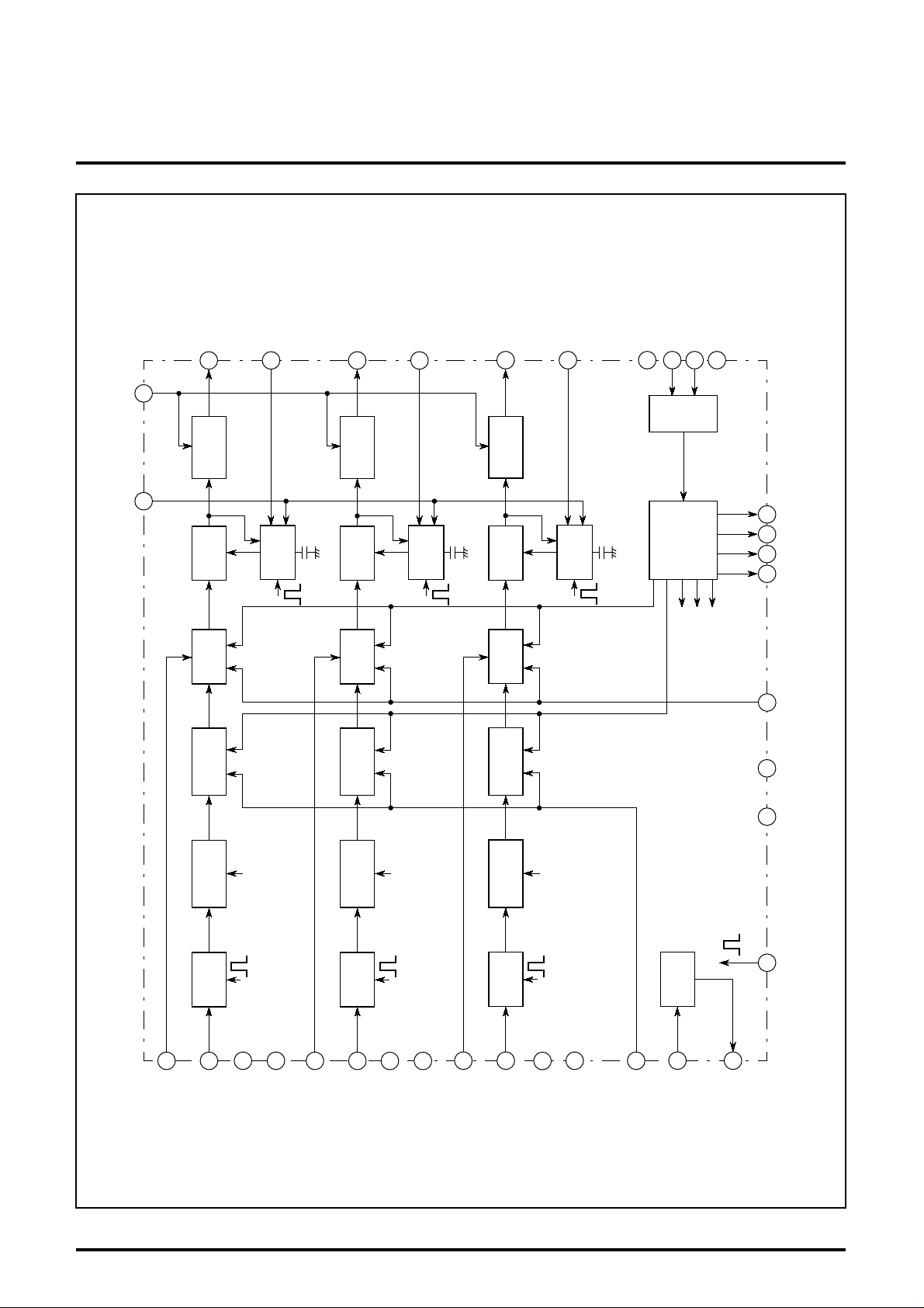
BLOCK DIAGRAM
27
OUTPUT (R)
35
RETRACE
BLANKING
EXT FEED BACK (R)
34
OUTPUT (G)
32
RETRACE
MITSUBISHI ICs (Monitor)
M52743BSP
2
I
C BUS CONTROLLED 3-CHANNEL VIDEO PREAMPLIFIER
VCC 5V
(DIGITAL)
SDA
SCL
21
BUS
I/F
20
GND(5V)
22
BLANKING
EXT FEED BACK (G)
31
OUTPUT (B)
29
RETRACE
BLANKING
EXT FEED BACK (B)
28
17
30
MAIN BRIGHTNESS RETRACE BLK IN
AMPOSD MIX
MAIN
CONTRAST
SUB
CONTRAST
F/B
CLAMP
(8bit)
SUB CONT
AMPOSD MIX
MAIN
CONTRAST
SUB
CONTRAST
F/B
CLAMP
(8bit)
SUB CONT
AMPOSD MIX
MAIN
CONTRAST
SUB
CONTRAST
F/B
CLAMP
OSD
Main
(8bit)
SUB CONT
4bit
LEVEL
8bit
CONTRAST
DAC
B SUB CONT 8bit
R SUB CONT 8bit
G SUB CONT 8bit
23 24 25 26
FOR CUT-OFF Adj
1
33
GND2 OSD BLK IN DAC OUTPUT
36
CC2=12V
V
CLAMP
2
4
INPUT (R)
OSD IN (R)
3
CC1 (R) 12V
V
5
GND 1(R)
CLAMP
6
9
INPUT (G)
OSD IN (G)
8
CC1 (G) 12V
V
10
GND 1(G)
CLAMP
11
13
INPUT (B)
OSD IN (B)
12
CC1 (B) 12V
V
14
GND 1(B)
Sync On
GreenSep
7
15
INPUT (SOG)
CONTRAST (ABL) IN
19
CLAMP PULSE
18
SOG SEP OUT
IN
2
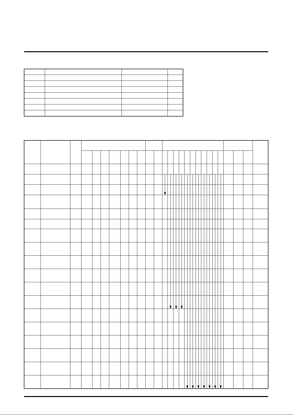
MITSUBISHI ICs (Monitor)
M52743BSP
2
I
C BUS CONTROLLED 3-CHANNEL VIDEO PREAMPLIFIER
ABSOLUTE MAXIMUM RATINGS
(Ta=25 ° C)
Symbol Parameter Ratings Unit
CC
V
P
d
T
opr
T
stg
V
opr
V
opr’
jc Case temperature 22
θ
ELECTRICAL CHARACTERISTICS
Symbol Parameter
CC1
I
I
CC2
Vomax
Vimax
Gv
∆ Gv
V
C1
∆ V
C1
V
C2
∆ V
C2
V
C3
∆ V
C3
V
SC1
∆ V
SC1
V
SC2
V
SC2
∆
V
SC3
V
SC3
∆
Supply voltage 13.0 V
Power dissipation 2403 mW
Ambient temperature -20 to +75
Storage temperature -40 to +150
Recommended supply 12.0 V
Voltage range 10.5 to 12.5 V
(V
CC
=12V, 5V, Ta=25 ° C, unless otherwise noted)
CTL
voltage
00H
15
30
Bright
Vari
able
Main
ABL
cont
FFH
255
5.0 6.0 8.0 − V
64H
100
FFH
255
C8H
200
64H
100
14H
20
FFH
255
FFH
255
FFH
255
Circuit
current1
Circuit
current2
Output
dynamic range
Maximum
input
Maximum
gain
Relative maximum gain
Main contrast
control
characteristics1
Main contrast
control relative
characteristics1
Main contrast
control
characteristics2
Main contrast
control relative
characteristics2
Main contrast
control
characteristics3
Main contrast
control relative
characteristics3
Sub contrast
control
characteristics1
Sub contrast
control relative
characteristics1
S
ub contrast
control
characteristics2
Sub contrast
control relative
characteristics2
Sub contrast
control
characteristics3
Sub contrast
control relative
characteristics3
Test
point
(s)
I
A
I
B
OUT
IN
OUT
OUT
2,6,11
OSD
RGB
BLK
in
aaa
aaa
b
SG2
b
SG2
Variable
b
SG1
4,9,13
1
OSD
in
aa
aa
aa
Input
19
CP in27ReT
b
SG5
b
SG5
b
SG5
b
SG5
b
SG5
7
SOG
in
BLK
a a 4.0 5.0
a a 4.0 5.0
aa
a a 2.0 5.0
a a 2.0 5.0
− −−−−−− −−−
OUT
b
SG1
aa
b
a a 2.0 5.0
SG5
− −−−−−− −−−
OUT
b
SG1
aa
b
a a 2.0 5.0
SG5
− −−−−−− −−−
OUT
b
SG1
aa
b
a a 2.0 5.0
SG5
− −−−−−− −−−
OUT
b
SG1
aa
b
a a 2.0 5.0
SG5
− − − − − − − − − −−−−
OUT
b
SG1
aa
b
a a 2.0 5.0
SG5
− − − − − − − − − −−−−
OUT
b
SG1
aa
b
a a 2.0 5.0
SG5
− − − − − − − − − −−−−
° C
° C
° C/W
BUS CTL (H) Limits
01H
02H
03H
04H
05H
06H
07H
08H
Sub
Sub
cont
cont
1
2
FFH
FFH
255
255
C8H
C8H
200
200
64H
64H
100
100
14H2014H2014H
Sub
cont
3
FFH
255
C8H
200
64H
100
20
OSD
BLK
Adj
Adj
OUT
00H000H0FFH
D/A
1
255
OUT
09H
D/A
D/A
D/A
OUT
OUT
2
3
4
FFH
FFH
FFH
255
255
255
0BH
INT
EXT
Min. Typ. Max.
00H
− 110 130 mA
0
− 18 22 mA
1.6 −− V
16.5 17.7 19.7 dB
0.8 1.0 1.2 −
14.5 16.0 17.5 dB
0.8 1.0 1.2 −
8.5 10.0 11.5 dB
0.8 1.0 1.2 −
0.2 0.4 0.6 V
0.8 1.0 1.2 −
14.8 16.3 17.8 dB
0.8 1.0 1.2 −
11.1 12.6 14.1 dB
0.8 1.0 1.2 −
1.4 1.7 2.0 V
0.8 1.0 1.2 −
Unit
P-P
P-P
P-P
P-P
3
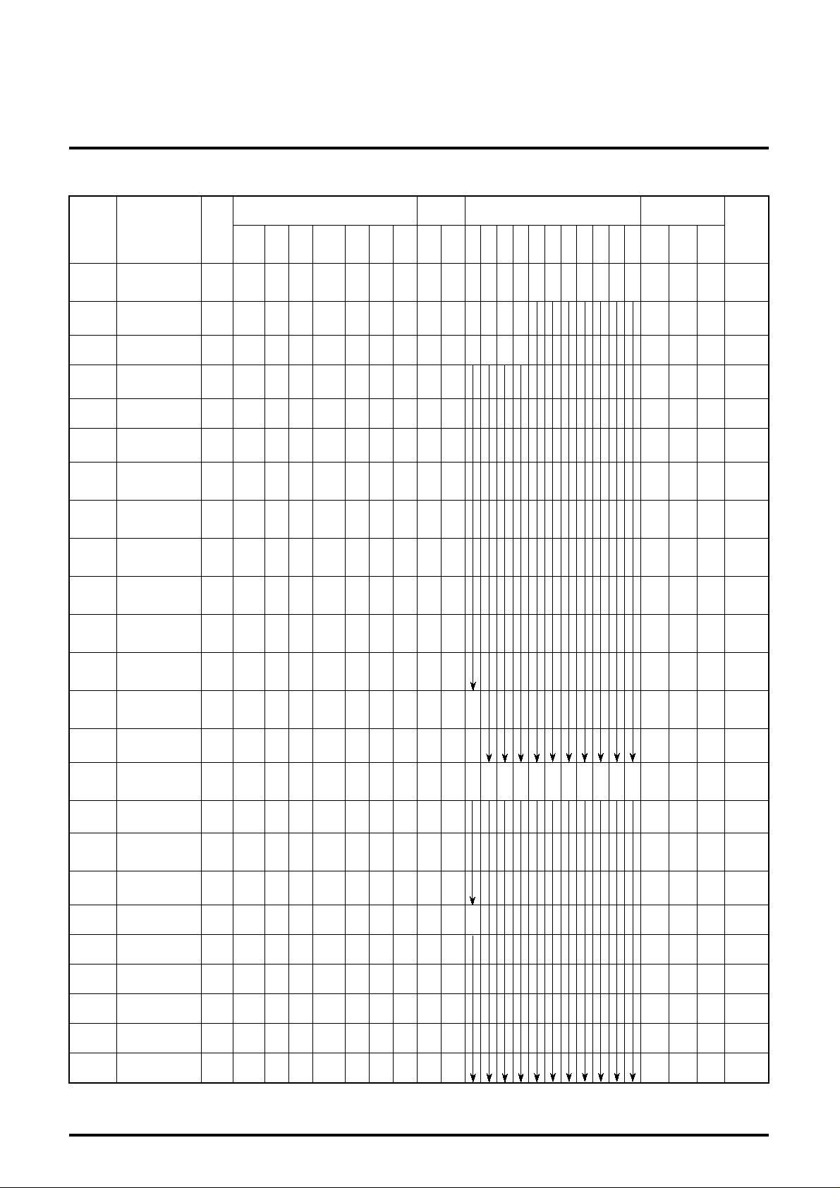
MITSUBISHI ICs (Monitor)
M52743BSP
2
I
C BUS CONTROLLED 3-CHANNEL VIDEO PREAMPLIFIER
ELECTRICAL CHARACTERISTICS
Test
Symbol Parameter
Main/sub
B1
C1’
C1’
contrast control
characteristics2
Main/sub contrast
control relative
characteristics2
ABL control
characteristics1
ABL control
relative
characteristics1
ABL control
characteristics2
ABL control
relative
characteristics2
Brightness
control
characteristics1
Brightness
control relative
characteristics1
Brightness
control
characteristics2
Brightness
control relative
characteristics2
Brightness
control
characteristics3
Brightness
control relative
characteristics3
Frequency
characteristics1
(f=50MHz)
Frequency relative
characteristics1
(f=50MHz)
Frequency
characteristics1
(f=150MHz)
Frequency relative
characteristics1
(f=150MHz)
Frequency
characteristics2
(f=150MHz)
Frequency relative
characteristics2
(f=150MHz)
Crosstalk 1
(f=50MHz)
Crosstalk 1
(f=150MHz)
Crosstalk 2
(f=50MHz)
Crosstalk 2
(f=150MHz)
Crosstalk 3
(f=50MHz)
Crosstalk 3
(f=150MHz)
VMSC
∆
VMSC
ABL1
∆ABL1
ABL2
∆ABL2
V
∆VB1
VB2
∆VB2
VB3
∆VB3
FC1
∆FC1
F
∆F
FC2
∆FC2
C.T.1
C.T.1’
C.T.2
C.T.2’
C.T.3
C.T.3’
point
(s)
OUT
2,6,11
RGB
in
b
SG1
4,9,13
1
OSD
BLK
aa
− − − − − − − − − −−−− 0.8 1.0 1.2 −
b
OUT
SG1
aa
− −−−−−− −− 0.8 1.0 1.2 −
b
OUT
SG1
aa
− −−−−−− −− 0.8 1.0 1.2 −
OUT a a a
− −−−−−− −− -0.3 0 0.3 −
OUT a a a
− −−−−−− −− -0.3 0 0.3 −
OUT a a a
− −−−−−− −− -0.3 0 0.3 −
b
OUT
SG3
aa
− −−−−−− −−− -1.0 0 1.0 dB
b
OUT
SG3
aa
− −−−−−− -1.0 0 1.0 dB
b
OUT
SG3
aa
− −−−−−− −− -1.0 0 1.0 dB
2bSG3
OUT(29)
6a
11a
2bSG3
6a
11a
2a
6bSG3
11a
2a
6bSG3
11a
2a
6a
11bSG3
2a
6a
11bSG3
aa
aa
aa
aa
aa
aa
OUT(32)
OUT(29)
OUT(32)
OUT(29)
OUT(35)
OUT(29)
OUT(35)
OUT(32)
OUT(35)
OUT(32)
OUT(35)
(cont.)
OSD
in
Input
19
CP in27ReT
b
SG5
b
SG5
b
SG5
b
SG5
b
SG5
b
SG5
a
5V
a
5V
a
5V
a
5V
a
5V
a
5V
a
5V
a
5V
a
5V
CTL
voltage
BLK
7
SOG
in
30
Bright
a a 2.0 5.0
a a 2.0 4.0
15
ABL
00H
Main
cont
C8H
200
FFH
255
BUS CTL (H) Limits
01H
02H
03H
04H
05H
06H
07H
08H
Sub
Sub
Sub
OSD
BLK
cont
cont
cont
1
2
3
C8H
C8H
C8H
200
200
200
FFH
FFH
FFH
255
255
255
Adj
Adj
OUT
00H000H0FFH
D/A
1
255
OUT
09H
D/A
D/A
D/A
OUT
OUT
2
3
4
FFH
FFH
FFH
255
255
255
0BH
INT
EXT
Min. Typ. Max.
00H
3.2 3.8 4.4 V
0
3.8 4.6 5.4 VP-P
a a 2.0 2.0 2.2 2.7 3.2 VP-P
a a 4.0 5.0 3.3 3.7 4.1 V
a a 2.0 5.0 1.5 1.8 2.1 V
a a 1.0 5.0 0.7 0.9 1.1 V
aa
aa
aa
aa
aa
aa
aa
aa
aa
Vari
able
Vari
able
Vari
able
Vari
able
Vari
able
Vari
able
Vari
able
Vari
able
Vari
able
Va
ria
5.0
5.0
ble
Va
ria
ble
FFH
FFH
FFH
255
00H000H0FFH
255
255
FFH
FFH
255
255
255
-2.0 0 2.5 dB
FFH
00H
-3.0 0 3.0 dB
255
0
5.0 -3.0 3.0 5.0 dB
FFH
5.0
255
− -25 -20 dB
5.0 − -15 -10 dB
5.0 − -25 -20 dB
5.0 − -15 -10 dB
5.0 − -25 -20 dB
5.0 − -15 -10 dB
Unit
P-P
4
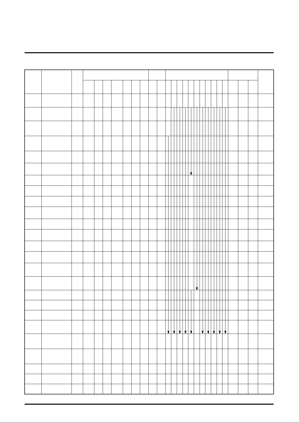
ELECTRICAL CHARACTERISTICS (cont.)
Symbol Parameter
Pulse
Tr
characteristics1
P-P)
(4V
Pulse
Tf
characteristics2
P-P)
(4V
Clamp pulse
VthCP
threshold
voltage
Clamp pulse
WCP
minimum
width
Pedestal voltage
DCL
temperature
characteristics1
Pedestal voltage
temperature
characteristics2
OSD pulse
characteristics1
OSD pulse
characteristics2
OSD adjust control
characteristics1
OSD adjust control
relative
characteristics1
OSD adjust control
characteristics2
OSD adjust control
relative
characteristics2
OSD adjust control
characteristics3
OSD adjust control
relative
characteristics3
PDCH
P
OTr
OTf
Oaj1
∆Oaj1
Oaj2
∆Oaj2
Oaj3
∆Oaj3
OSD input
VthOSD
threshold
voltage
OSD BLK input
VthBLK
HBLK1
HBLK2
HBLK3
threshold
voltage
Retrace BLK
characteristics1
Retrace BLK
characteristics2
Retrace BLK
characteristics3
Retrace BLK
VthRET
input threshold
voltage
SOG input
SS-NV
maximum
noize voltage
SOG
SS-SV
minimum
input voltage
VSH
VSL
TDS-F
Sync output
hi level
Sync output
lo level
Sync output
delay time1
Test
point
2,6,11
(s)
OUT
OUT
OUT
OUT
OUT
OUT
RGB
in
b
SG1
b
SG1
b
SG1
b
SG1
b
SG1
b
SG1
OSD
BLK
OUT a a
OUT a a
OUT a
SG6bSG6
− −−−−−− −− − 0.8 1.0 1.2 −
OUT a
SG6bSG6
− −−−−−− −− − 0.8 1.0 1.2 −
OUT a
SG6bSG6
− −−−−−− −− − 0.8 1.0 1.2 −
OUT a
OUT
b
SG1
SG6
SG6
Variable
OUT a a a
OUT a a a
OUT a a a
OUT a a a
SonG
IN
aaaaa
Sync
OUT
SonG
IN
aaaaa
Sync
OUT
Sync
aaaaa
OUT
Sync
aaaaa
OUT
Sync
aaaaa
OUT
4,9,13
1
OSD
in
aa
aa
aa
aa
aa
aa
b
SG6
b
SG6
b
b
b
b
b
SG6
Variable
b
a
Input
CP in27ReT
SG5
SG5
SG5
Variable
SG5
Variable
SG5
SG5
SG5
SG5
SG5
SG5
SG5
SG5
SG5
SG5
SG5
SG5
SG5
MITSUBISHI ICs (Monitor)
M52743BSP
I2C BUS CONTROLLED 3-CHANNEL VIDEO PREAMPLIFIER
CTL
voltage
19
b
b
b
b
b
b
b
b
b
b
b
b
b
b
b
b
b
SOG
BLK
aa
aa
7
in
30
Bright
Vari
able
Vari
able
a a 2.0 5.0
a a 2.0 5.0 0.2 0.5 −µs
a a 2.0 5.0 -3.0 0 0.3 V
a a 2.0 5.0 -3.0 0 0.3 V
a a 2.0 5.0
a a 2.0 5.0
a a 2.0 5.0
a a 2.0 5.0
a a 2.0 5.0
a a 2.0 5.0
a a 2.0 5.0
b
a 2.0 5.0
SG7
b
a 2.0 5.0
SG7
b
a 2.0 5.0
SG7
b
a 2.0 5.0
SG7
Variable
b
SG4
Variable
b
SG4
Variable
b
SG4
b
SG4
b
SG4
2.0 5.0 0 0.01 0.02 VP-P
2.0 5.0 0.2 0.3 − VP-P
2.0 5.0 4.5 4.9 5.0 V
2.0 5.0 0 0.3 0.6 V
2.0 5.0 0 60 90 ns
15
ABL
5.0
5.0
00H
Main
cont
Va
ria
ble
Va
ria
ble
FFH
255
BUS CTL (H) Limits
01H
02H
03H
04H
05H
06H
07H
08H
Sub
cont
FFH
255
Sub
Sub
OSD
BLK
Adj
Adj
OUT
00H000H0FFH
08H
8
08H
8
0FH
15
08H
8
08H
8
08H
8
00H
0
0FH
15
06H
6
00H
0
08H
8
D/A
1
255
cont
cont
1
2
3
FFH
FFH
255
255
OUT
09H
D/A
D/A
D/A
OUT
OUT
2
3
4
FFH
FFH
FFH
255
255
255
0BH
INT
EXT
Min. Typ. Max.
00H
− 1.7 − ns
0
− 3.0 − ns
1.0 1.5 2.0 V
− 3.0 6.0 ns
− 3.0 6.0 ns
4.6 5.4 6.2 VP-P
2.8 3.3 3.8 VP-P
0 0.1 0.5 VP-P
2.2 2.7 3.2 V
2.2 2.7 3.2 V
1.7 2.0 2.3 V
0.7 1.0 1.3 V
0.1 0.4 0.7 V
1.0 1.5 2.0 V
Unit
5
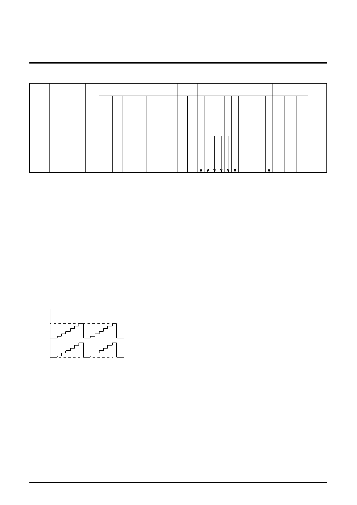
ELECTRICAL CHARACTERISTICS (cont.)
VC1=20Log (dB)
VOUT
0.7
Input
4,9,13
1
OSD
CP in27ReT
in
Symbol Parameter
TDS-R
VOH
VOL
IAO
DNL
Sync output
delay time2
D/A H output
voltage
D/A L output
voltage
D/A output
current range
D/A
nonlinearity
Test
point
2,6,11
(s)
Sync
OUT
D/A
OUT
D/A
OUT
D/A
OUT
D/A
OUT
OSD
RGB
BLK
in
aaaaa
aaaaa
aaaaa
aaaaa
aaaaa
MITSUBISHI ICs (Monitor)
M52743BSP
I2C BUS CONTROLLED 3-CHANNEL VIDEO PREAMPLIFIER
CTL
voltage
15
ABL
00H
Main
cont
FFH
255
BLK
7
SOG
in
b
SG4
a
a
a
a
30
Bright
2.0 5.0 0 60 90 ns
2.0 5.0
2.0 5.0
2.0 5.0
2.0 5.0
19
BUS CTL (H) Limits
01H
02H
03H
04H
05H
06H
07H
08H
Sub
cont
FFH
255
Sub
Sub
OSD
BLK
Adj
Adj
OUT
00H000H0FFH
Vari
Vari
D/A
1
255
00H000H000H000H
abl
e
abl
e
cont
cont
1
2
3
FFH
FFH
255
255
OUT
Vari
Vari
09H
D/A
D/A
D/A
OUT
OUT
2
3
4
FFH
FFH
FFH
255
255
255
0
Vari
Vari
abl
abl
abl
e
e
e
Vari
Vari
abl
abl
abl
e
e
e
0BH
INT
EXT
Min. Typ. Max.
00H
4.5 5.0 5.5 VDC
0
0 0.5 1.0 VDC
-1.0 − 0.4 mA
-1.0 − 1.0 LSB
Unit
ELECTRICAL CHARACTERISTICS TEST METHOD
ICC1 Circuit current1
Measuring conditions are as listed in supplementary Table.
Mesured with a current meter at test point IA.
CC2 Circuit current2
I
Measureing conditions are as listed in supplemtary Table.
Measured with a current meter at test point IB.
Vomax Output dynamic range
Decrease V30 gradually, and measure the voltage when the bottom
of waveform output is distorted. The voltage is called VCL.
Next, increase V30 gradually, and measure the voltage when the
top of waveform output is distorted. The voltage is called VOH.
Voltage Vomax is calculated by the equation below:
Vomax = VOH-VOL
(V)
VOH
5.0
Waveform output
VOL
0.0
Vimax Maximum input
Increase the input signal (SG2) amplitude gradually, starting from
700mV
P-P. Measure the amplitude of the input signal when the
output signal starts becoming distorted.
Gv Maximum gain
Input SG1, and read the amplitude output at OUT (29, 32, 35). The
amplitude is called VOUT (29, 32, 35). Maximum gain G
calculated by the equation below:
GV=20Log (dB)
VOUT
0.7
V is
∆Gv Relative maximum gain
Relative maximum gain ∆G
∆G
V is calculated by the equation bellow:
V= VOUT (29)/VOUT (32),
VOUT (32)/VOUT (35),
VOUT (35)/VOUT (29)
C1 Main contrast control characteristics1
V
Measureing the amplitude output at OUT (29, 32, 35). The
measured value is called VOUT (29, 32, 35). Main contrast control
characterics V
C1 is calculated by the equation bellow:
∆VC1 Main contrast control relative characteristics1
Relative characteristics ∆VC1 is calculated by the equation bellow:
∆VC1=VOUT (29)/VOUT (32),
VOUT (32)/VOUT (35),
VOUT (35)/VOUT (29)
V
C2 Main contrast control characteristics2
Measuring condition and procedure are the same as described in
C1.
V
∆V
C2 Main contrast control relative characteristics2
Measuring condition and procedure are the same as described in
∆VC1.
V
C3 Main contrast control characteristics3
Measuring condition and procedure are the same as described in
C1.
V
∆VC3 Main contrast control relative characteristics3
Measuring condition and procedure are the same as described in
∆VC1.
6
 Loading...