

MITSUBISHI ICs (Monitor)
PRELIMINARY
Notice:This is not a final specification.
Some parametric limits are subject to change.
DESCRIPTION
M52742ASP is semiconductor integrated circuit for CRT display
monitor.
It includes OSD blanking, OSD mixing, retrace blanking, wide band
amplifer, brightness control, uniformity function.
Main/sub contrast and OSD adjust function can be controlled by I2C
bus.
FEATURES
• Frequency band width: RGB.............................200MHz (at -3dB)
Input :RGB.............................................................0.7VP-P (typ.)
OSD..........................................3VP-P minimum (positive)
BLK (for OSD)..........................3VP-P minimum (positive)
Retrace BLK.............................3VP-P minimum (positive)
Output :RGB..........................................................5.5VP-P (max.)
OSD..............................................................5VP-P (max.)
• Main contrast and sub contrast can be controlled by I
• Include internal and external pedestal clamp circuit
STRUCTURE
Bipolar silicon monolithic IC
APPLICATION
CRT display monitor
BUS CONTROLLED 3-CHANNEL VIDEO PREAMP FOR CRT DISPLAY MONITOR
OSD..............................................80MHz
2
C bus.
M52742ASP
PIN CONFIGURATION (TOP VIEW)
OSD BLK IN
INPUT(R)
VCC1(R)
OSD IN(R)
GND 1(R)
INPUT(G)
INPUT(SOG)
VCC1(G)
OSD IN(G)
GND 1(G)
INPUT(B)
VCC1(B)
OSD IN(B)
GND 1(B)
ABL IN
UNIFORMITY IN
VCC=5V
SOG SEP OUT
1
2
3
4
7
8
13
14
15 22
16 21
17
18 19
36
VCC2
OUTPUT(R)
35
EXT FEED BACK(R)
34
GND2
33
325
OUTPUT(G)
316
EXT FEED BACK(G)
MAIN BRIGHTNESS
30
M52742ASP
OUTPUT(B)
29
EXT FEED BACK(B)
289
2710
RETRACE BLK IN
2611
D/A OUT1
2512
D/A OUT2
D/A OUT3
24
D/A OUT4
23
GND(5V)
SDA
20
SCL
CLAMP PULSE IN
RECOMMENDED OPERATING CONDITION
Supply voltage range......................11.5 to 12.5V (V3, V8, V12, V36)
4.5 to 5.5V (V17)
Rated supply voltage..................................12.0V (V3, V8, V12, V36)
5.0V (V17)
MAJOR SPECIFICATION
Bus controlled 3ch video pre-amp with OSD mixing function and
retrace blanking function
Outline 36P4E
1
MITSUBISHI ICs (Monitor)
PRELIMINARY
Notice:This is not a final specification.
Some parametric limits are subject to change.
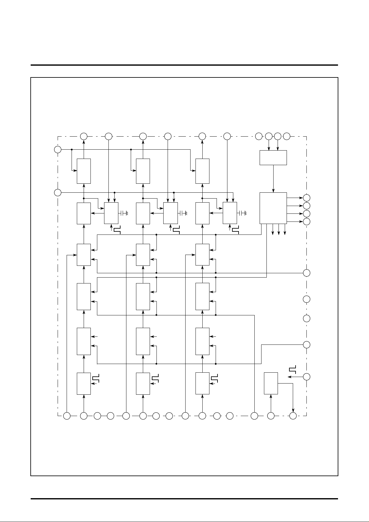
BLOCK DIAGRAM
OUTPUT (R)
35
27
RETRACE BLK IN
RETRACE
BLANKING
30
MAIN BRIGHTNESS
AMP
M52742ASP
BUS CONTROLLED 3-CHANNEL VIDEO PREAMP FOR CRT DISPLAY MONITOR
Vcc 5V
EXT FEED BACK (R)
34
CLAMP
F/B
OUTPUT (G)
32
RETRACE
AMP
BLANKING
EXT FEED BACK (G)
31
F/B
CLAMP
OUTPUT (B)
29
RETRACE
AMP
BLANKING
EXT FEED BACK (B)
28
F/B
CLAMP
(DIGITAL)
SDA
17
21
BUS
DAC
SCL
20
I/F
GND(5V)
22
26
2524
DAC OUTPUT
23
FOR CUT-OFF adj
4bit
OSD
LEVEL
B SUB CONT 8bit
R SUB CONT 8bit
OSD MIX
MAIN
CONTRAST
SUB
CONTRAST
CLAMP
2
4
(8bit)
SUB CONT
3
5
OSD MIX
MAIN
CONTRAST
SUB
CONTRAST
CLAMP
9
6
(8bit)
SUB CONT
8
10
OSD MIX
8bit
(8bit)
SUB CONT
14
12
Main
CONTRAST
15
MAIN
CONTRAST
SUB
CONTRAST
CLAMP
11
13
G SUB CONT 8bit
Sync On
GreenSep
7
1
OSD BLK IN
33
GND2
36
Vcc2=12V
1619
IN
UNIFORMITY
IN
CLAMP PULSE
18
INPUT (R)
OSD IN (R)
Vcc1 (R) 12V
GND 1(R)
INPUT (G)
OSD IN (G)
Vcc1 (G) 12V
GND 1(G)
INPUT (B)
OSD IN (B)
Vcc1 (B) 12V
GND 1(B)
INPUT (SOG)
CONTRAST (ABL) IN
SOG SEP OUT
2
MITSUBISHI ICs (Monitor)
PRELIMINARY
Notice:This is not a final specification.
Some parametric limits are subject to change.
ABSOLUTE MAXIMUM RATINGS (Ta=25°C)
Symbol Parameter Ratings Unit
VCC12 Supply voltage (pins 3,8,12,36) 13.0
VCC5 Supply voltage (pin 17) 6.0
Pd Power dissipation 2403 mW
Topr Ambient temperature -20 to +75 C
Tstg Storage temperature -40 to +150 C
Vopr12 Recommended supply 12 12.0 V
Vopr5 5.0 V
Recommended supply 5
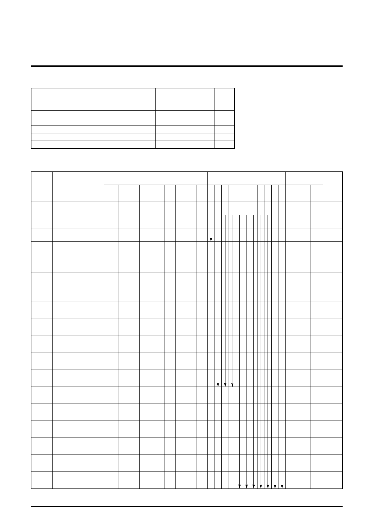
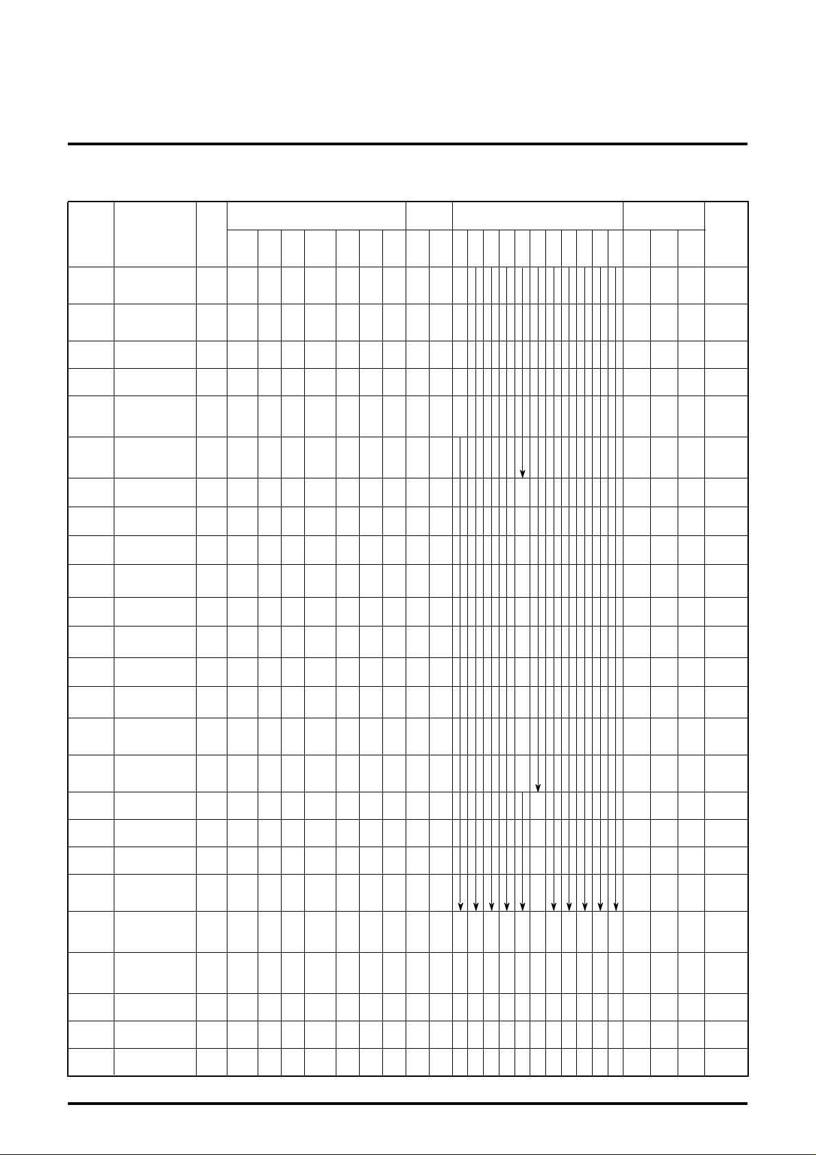
ELECTRICAL CHARACTERISTICS (VCC=12V, 5V, Ta=25°C, unless otherwise noted)
Symbol Parameter
ICC1
ICC2
Vomax
Vimax
Gv
∆Gv
VC1
∆VC1
VC2
∆VC2
VC3
∆VC3
VSC1
∆VSC1
VSC2
∆VSC2
VSC3
∆VSC3
Circuit
current1
Circuit
current2
Output
dynamic range
Maximum
input
Maximum
gain
Relative maximum gain
Main contrast
control
characteristics1
Main contrast
control relative
characteristics1
Main contrast
control
characteristics2
Main contrast
control relative
characteristics2
Main contrast
control
characteristics3
Main contrast
control relative
characteristics3
Sub contrast
control
characteristics1
Sub contrast
control relative
characteristics1
Sub contrast
control
characteristics2
Sub contrast
control relative
characteristics2
Sub contrast
control
characteristics3
Sub contrast
control relative
characteristics3
BUS CONTROLLED 3-CHANNEL VIDEO PREAMP FOR CRT DISPLAY MONITOR
V
V
°
°
Test
point
2,6,11
(s)
RGB
in
OSD
BLK
IA a a a
IB a a a
b
OUT
SG2
b
IN
SG2
OUT
Variable
b
OUT
SG1
4,9,13
1
OSD
a a
a a
a a
Input
in
19
CP in27ReT
b
SG5
b
SG5
b
SG5
b
SG5
b
SG5
7
SOG
in
BLK
a a a 4.0 5.0
a a a 4.0 5.0 - 18 25 mA
a a a
a a a 2.0 5.0
a a a 2.0 5.0
- - - - - - - - - - - 0.8 1.0 1.2 -
OUT
b
SG1
a a
b
a a a 2.0 5.0
SG5
- - - - - - - - - - - 0.8 1.0 1.2 -
OUT
b
SG1
a a
b
a a a 2.0 5.0
SG5
- - - - - - - - - - - 0.8 1.0 1.2 -
OUT
b
SG1
a a
b
a a a 2.0 5.0
SG5
- - - - - - - - - - - 0.8 1.0 1.2 -
OUT
b
SG1
a a
b
a a a 2.0 5.0
SG5
- - - - - - - - - - - - - - 0.8 1.0 1.2 -
OUT
b
SG1
a a
b
a a a 2.0 5.0
SG5
- - - - - - - - - - - - - - 0.8 1.0 1.2 -
OUT
b
SG1
a a
b
a a a 2.0 5.0
SG5
- - - - - - - - - - - - - - 0.8 1.0 1.2 -
16
UNI
in
CTL
voltage
00H
15
30
Bright
Vari
able
Main
ABL
cont
FFH
255
5.0 6.0 8.0 - VP-P
64H
100
FFH
255
C8H
200
64H
100
14H
20
FFH
255
FFH
255
FFH
255
BUS CTL (H) Limits
01H
02H
03H
Sub
cont
FFH
C8H
64H
255
200
100
2
04H
Sub
OSD
cont
3
FFH
00H000H0FFH
255
C8H
200
64H
100
20
Sub
cont
1
FFH
255
C8H
200
64H
100
14H2014H2014H
M52742ASP
05H
06H
07H
BLK
D/A
Adj
D/A
Adj
OUT
OUT
1
2
FFH
255
255
08H
OUT
FFH
255
0BH
09H
INT
D/A
D/A
EXT
Min. Typ. Max.
OUT
3
4
FFH
00H
- 126 146 mA
255
0
1.6 - - VP-P
16.5 17.7 19.4 dB
15.5 17.0 18.5 dB
9.5 11.0 12.5 dB
0.2 0.4 0.6
16.0 17.5 19.0 dB
12.0 13.5 15.0 dB
1.5 1.9 2.2
Unit
V
V
P-P
P-P
3
MITSUBISHI ICs (Monitor)
PRELIMINARY
Notice:This is not a final specification.
Some parametric limits are subject to change.
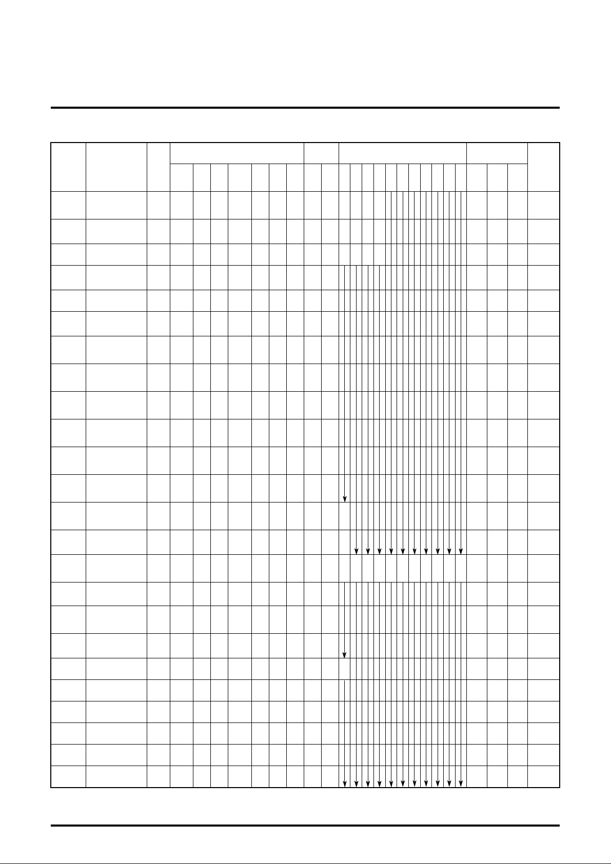
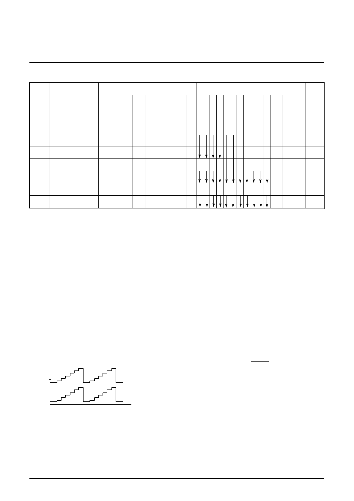
ELECTRICAL CHARACTERISTICS (cont.)
Symbol Parameter
VMSC
∆VMSC
ABL1
∆ABL1
ABL2
∆ABL2
VB1
∆VB1
VB2
∆VB2
VB3
∆VB3
FC1
∆FC1
FC1’
∆FC1’
FC2
∆FC2
C.T.1
C.T.1’
C.T.2
C.T.2’
C.T.3
C.T.3’
Main/sub
contrast control
characteristics
Main/sub contrast
control relative
characteristics
ABL control
characteristics1
ABL control
relative
characteristics1
ABL control
characteristics2
ABL control
relative
characteristics2
Brightness
control
characteristics1
Brightness
control relative
characteristics1
Brightness
control
characteristics2
Brightness
control relative
characteristics2
Brightness
control
characteristics3
Brightness
control relative
characteristics3
Frequency
characteristics1
(f=50MHz)
Frequency relative
characteristics1
(f=50MHz)
Frequency
characteristics1
(f=200MHz)
Frequency relative
characteristics1
(f=200MHz)
Frequency
characteristics2
(f=200MHz)
Frequency relative
characteristics2
(f=200MHz)
Crosstalk 1
(f=50MHz)
Crosstalk 1
(f=200MHz)
Crosstalk 2
(f=50MHz)
Crosstalk 2
(f=200MHz)
Crosstalk 3
(f=50MHz)
Crosstalk 3
(f=200MHz)
BUS CONTROLLED 3-CHANNEL VIDEO PREAMP FOR CRT DISPLAY MONITOR
Test
point
2,6,11
(s)
OUT
RGB
in
b
SG1
OSD
BLK
- - - - - - - - - - - - - - 0.8 1.0 1.2 b
OUT
SG1
- - - - - - - - - - 0.8 1.0 1.2 b
OUT
SG1
- - - - - - - - - - 0.8 1.0 1.2 -
OUT a a a
- - - - - - - - - - -0.3 0 0.3 V
OUT a a a
- - - - - - - - - - -0.3 0 0.3 V
OUT a a a
- - - - - - - - - - -0.3 0 0.3 V
b
OUT
SG3
- - - - - - - - - - - -1.0 0 1.0 dB
b
OUT
SG3
- - - - - - - - -1.0 0 1.0 dB
b
OUT
SG3
- - - - - - - - - - -1.0 0 1.0 dB
2bSG3
OUT(29)
6a
OUT(32)
11a
2bSG3
OUT(29)
6a
OUT(32)
11a
2a
OUT(29)
6bSG3
OUT(35)
11a
2a
OUT(29)
6bSG3
OUT(35)
11a
2a
OUT(32)
6a
OUT(35)
11bSG3
2a
OUT(32)
6a
OUT(35)
11bSG3
4,9,13
1
OSD
a a
a a
a a
a a
a a
a a
a a
a a
a a
a a
a a
a a
Input
in
CP in27ReT
SG5
SG5
SG5
SG5
SG5
SG5
M52742ASP
CTL
voltage
19
b
b
b
b
b
b
a
5V
a
5V
a
5V
a
5V
a
5V
a
5V
a
5V
a
5V
a
5V
7
16
BLK
SOG
in
UNI
in
30
Bright
a a a 2.0 5.0
a a a 2.0 4.0
a a a 2.0 2.0 2.6 3.1 3.6 VP-P
a a a 4.0 5.0 3.3 3.7 4.1 V
a a a 2.0 5.0 1.5 1.8 2.1 V
a a a 1.0 5.0 0.7 0.9 1.1 V
a a a
a a a
a a a
a a a
a a a
a a a
a a a
a a a
a a a
Vari
able
Vari
able
Vari
able
Vari
able
Vari
able
Vari
able
Vari
able
Vari
able
Vari
able
00H
15
Main
ABL
cont
C8H
200
FFH
255
Va
5.0
ria
ble
Va
5.0
ria
ble
5.0 -3.0 3.0 5.0 dB
FFH
5.0
255
5.0 - -15 -10 dB
5.0 - -25 -20 dB
5.0 - -15 -10 dB
5.0 - -25 -20 dB
5.0 - -15 -10 dB
BUS CTL (H) Limits
01H
02H
03H
04H
05H
06H
07H
08H
Sub
Sub
Sub
OSD
BLK
cont
cont
cont
1
2
3
C8H
C8H
C8H
200
200
200
FFH
FFH
FFH
255
255
255
FFH
FFH
FFH
255
255
255
Adj
Adj
00H000H0FFH
OUT
D/A
255
09H
D/A
D/A
D/A
OUT
OUT
1
OUT
2
3
4
FFH
FFH
FFH
255
255
255
0BH
INT
EXT
Min. Typ. Max.
3.5 4.1 4.7 VP-P
4.7 5.0 5.8 VP-P
-2.0 0 2.5 dB
00H
-3.0 0 3.0 dB
0
- -25 -20 dB
Unit
4
MITSUBISHI ICs (Monitor)
PRELIMINARY
Notice:This is not a final specification.
Some parametric limits are subject to change.
ELECTRICAL CHARACTERISTICS (cont.)
Symbol Parameter
Tr
Pulse
characteristics1
(4VP-P)
Pulse
characteristics2
(4VP-P)
Relative pulse
characteristics1
Relative pulse
characteristics2
Clamp pulse
threshold
voltage
Clamp pulse
minimum
width
OSD pulse
characteristics1
OSD pulse
characteristics2
OSD adjust control
characteristics1
OSD adjust control
relative
characteristics1
OSD adjust control
characteristics2
OSD adjust control
relative
characteristics2
OSD adjust control
characteristics3
OSD adjust control
relative
characteristics3
OSD input
threshold
voltage
OSD BLK input
threshold
voltage
Retrace BLK
characteristics1
Retrace BLK
characteristics2
Retrace BLK
characteristics3
Retrace BLK
input threshold
voltage
SOG input
maximum
noise voltage
SOG
minimum
input voltage
Sync output
hi level
Sync output
lo level
Sync output
delay time1
Tr
Tf
Tr
∆
∆
VthCP
WCP
OTr
OTf
Oaj1
∆Oaj1
Oaj2
∆Oaj2
OBLK
∆OBLK
VthOSD
VthBLK
HBLK1
HBLK2
HBLK3
VthRET
SS-NV
SS-SV
VSH
VSL
TDS-F
BUS CONTROLLED 3-CHANNEL VIDEO PREAMP FOR CRT DISPLAY MONITOR
Test
point
2,6,11
(s)
OUT
OUT
OUT
OUT
OUT
OUT
RGB
in
b
SG1
b
SG1
b
SG1
b
SG1
b
SG1
b
SG1
OSD
BLK
OUT a a
OUT a a
OUT a
SG6bSG6
- - - - - - - - - - - 0.8 1.0 1.2 -
OUT a
SG6bSG6
- - - - - - - - - - - 0.8 1.0 1.2 -
OUT a
SG6
- - - - - - - - - - - -0.2 0 0.2 VP-P
OUT a
OUT
b
SG1
SG6
SG6
Variable
OUT a a a
OUT a a a
OUT a a a
OUT a a a
SonG IN
Sync OUT
Sync OUT
Sync OUT
Sync OUT
Sync OUT
a a a a a
SonG IN
a a a a a
a a a a a
a a a a a
a a a a a
Input
4,9,13
1
OSD
CP in27ReT
in
a a
a a
a a
a a
a a
a a a a a 2.0 5.0
SG5
SG5
SG5
SG5
SG5
Variable
SG5
Variable
b
SG6
SG5
b
SG6
SG5
b
SG5
b
SG5
b
a
SG5
b
b
SG6
SG5
Variable
b
a
SG5
SG5
SG5
SG5
SG5
M52742ASP
CTL
voltage
19
b
b
b
b
7
SOG
in
BLK
a a a
a a a
a a a
a a a
b
a a a 2.0 5.0
16
UNI
in
30
Bri-
ght
Vari
able
Vari
able
Vari
able
Vari
able
15
ABL
5.0
5.0
5.0
5.0
00H
Main
cont
Va
ria
ble
Va
ria
ble
Vari
able
Vari
able
FFH
255
b
b
a a a 2.0 5.0 - 3.0 6.0 ns
b
a a a 2.0 5.0
b
a a a 2.0 5.0
b
a a a 2.0 5.0
b
a a a 2.0 5.0
b
a a a 2.0 5.0
b
a a a 2.0 5.0
b
b
a a 2.0 5.0
SG7
b
b
a a 2.0 5.0
SG7
b
b
a a 2.0 5.0
SG7
b
b
a a 2.0 5.0
SG7
Variable
b
SG4
Variable
b
SG4
Variable
b
SG4
b
SG4
b
SG4
a 2.0 5.0 - - 0.02 VP-P
a 2.0 5.0 0.2 0.3 - VP-P
a 2.0 5.0 4.5 4.9 5.0 V
a 2.0 5.0 0 0.3 0.6 V
a 2.0 5.0 0 60 90 ns
BUS CTL (H) Limits
01H
02H
03H
04H
05H
06H
07H
08H
Sub
cont
Sub
Sub
OSD
BLK
cont
cont
1
2
3
D/A
Adj
Adj
OUT
1
08H
8
08H
8
0FH
15
08H
8
00H
0
08H
8
00H
0
0FH
15
06H
6
00H
0
08H
8
D/A
OUT
09H
D/A
D/A
OUT
OUT
2
3
0BH
INT
EXT
Min. Typ. Max.
4
- 1.7 - ns
- 2.2 - ns
-0.8 0 0.8 ns
-0.8 0 0.8 ns
1.0 1.5 2.0 V
0.2 0.5 -
- 3.0 6.0 ns
4.6 5.4 6.2 VP-P
2.8 3.3 3.8 VP-P
0 -0.1 -0.3 VP-P
2.2 2.7 3.2 V
2.2 2.7 3.2 V
1.7 2.0 2.3 V
0.7 1.0 1.3 V
0.1 0.4 0.7 V
1.0 1.5 2.0 V
Unit
µs
5
MITSUBISHI ICs (Monitor)
PRELIMINARY
Notice:This is not a final specification.
Some parametric limits are subject to change.
ELECTRICAL CHARACTERISTICS (cont.)
Symbol Parameter
TDS-R
VOH
VOL
DNL
UNI1
UNI2
1A-
1A+
Sync output
delay time2
D/A H output
voltage
D/A L output
voltage
D/A
nonlinearity
Uniformity
characteristics1
Uniformity
characteristics2
D/A input
current range
D/A output
current range
BUS CONTROLLED 3-CHANNEL VIDEO PREAMP FOR CRT DISPLAY MONITOR
Test
point
(s)
Sync OUT
D/A
OUT
D/A
OUT
D/A
OUT
OUT
OUT
D/A
OUT
D/A
OUT
2,6,11
OSD
RGB
BLK
in
a a a a a
a a a a a a a 2.0 5.0
a a a a a a a 2.0 5.0
a a a a a a a 2.0 5.0
b
SG1
b
SG1
a a a
a a a
4,9,13
1
a a
a a
OSD
in
Input
CP in27ReT
SG5
SG5
19
b
b
a
a
7
SOG
in
BLK
b
SG4
a a 5.0
a a 5.0
a a a 2.0 5.0
a a a
M52742ASP
CTL
voltage
16
UNI
in
30
Bright
15
ABL
00H
Main
cont
a 2.0 5.0 0 60 90 ns
FFH
255
b
SG6
2.5V
b
SG6
1.25V
2.0
2.0
C8H
200
00H
0
2.0 5.0
BUS CTL (H) Limits
01H
02H
03H
04H
05H
06H
07H
08H
Sub
Sub
Sub
OSD
BLK
cont
cont
cont
1
2
3
FFH
FFH
FFH
255
255
255
C8H
C8H
C8H
200
200
200
00H
00H
00H
0
0
0
Adj
Adj
00H000H0FFH
00H
00H
0
0
D/A
OUT
255
00H000H000H000H
Vari
able
FFH
255
00H
0
09H
D/A
D/A
D/A
OUT
OUT
FFH
255
Vari
able
FFH
255
00H
0
OUT
2
3
4
FFH
FFH
255
255
0
Vari
Vari
able
able
FFH
FFH
255
255
00H
00H
0
0
1
0BH
INT
EXT
Min. Typ. Max.
00H
4.5 5.0 5.5 VDC
0
0 0.5 1.0 VDC
-1.0 - 1.0 LSB
7 10 13 %
3.5 5 6.5 %
00H
0
0.18
- -
-
-
1.0
Unit
mA
mA
ELECTRICAL CHARACTERISTICS TEST METHOD
ICC1 Circuit current1
Measuring conditions are as listed in supplementary Table.
Measured with a current meter at test point IA.
ICC2 Circuit current2
Measuring conditions are as listed in supplementary Table.
Measured with a current meter at test point IB.
Vomax Output dynamic range
Decrease V30 gradually, and measure the voltage when the
waveform output is distorted. The voltage is called VOL.
Next, increase V30 gradually, and measure the voltage when the
top of waveform output is distorted. The voltage is called VOH.
Voltage Vomax is calculated by the equation below:
Vomax = VOH-VOL
(V)
VOH
5.0
Waveform output
VOL
0.0
Gv Maximum gain
Input SG1, and read the amplitude output at OUT (29, 32, 35). The
amplitude is called VOUT (29, 32, 35). Maximum gain GV is
calculated by the equation below:
VOUT
GV=20Log
0.7
(dB)
∆Gv Relative maximum gain
Relative maximum gain DGV is calculated by the equation bellow:
∆GV= VOUT (29)/VOUT (32),
VOUT (32)/VOUT (35),
VOUT (35)/VOUT (29)
VC1 Main contrast control characteristics1
Measuring the amplitude output at OUT (29, 32, 35). The
measured value is called VOUT (29, 32, 35). Main contrast control
characterics VC1 is calculated by the equation bellow:
VOUT
VC1=20Log
0.7
(dB)
∆VC1 Main contrast control relative characteristics1
Relative characteristics ∆VC1 is calculated by the equation bellow:
∆VC1=VOUT (29)/VOUT (32),
VOUT (32)/VOUT (35),
VOUT (35)/VOUT (29)
Vimax Maximum input
Increase the input signal (SG2) amplitude gradually, starting from
700mVP-P. Measure the amplitude of the input signal when the
output signal starts becoming distorted.
VC2 Main contrast control characteristics2
Measuring condition and procedure are the same as described in
VC1.
∆VC2 Main contrast control relative characteristics2
Measuring condition and procedure are the same as described in
∆VC1.
6

MITSUBISHI ICs (Monitor)
PRELIMINARY
Notice:This is not a final specification.
Some parametric limits are subject to change.
VC3 Main contrast control characteristics3
Measuring the amplitude output at OUT (29, 32, 35).
The measured value is called VOUT (29, 32, 35).
∆VC3 Main contrast control relative characteristics3
Measuring condition and procedure are the same as described in
∆VC1.
VSC1 Sub contrast control characteristics1
Measure the amplitude output at OUT (29, 32, 35). The measured
value is called VOUT (29, 32, 35). Sub contrast control
characteristics VSC1 is calculated by the equation below:
VSC1=20Log
∆VSC1 Sub contrast control relative characteristics1
Relative characteristics ∆VSC1 is calculated by the equation below:
∆VSC1=VOUT (29)/VOUT (32),
VSC2 Sub contrast control characteristics2
Measuring condition and procedure are the same as described in
VSC1.
∆VSC2 Sub contrast control relative characteristics2
Measuring condition and procedure are the same as described in
∆VSC1.
VSC3 Sub contrast control characteristics3
Measuring the amplitude output at OUT (29, 32, 35).
The measured value is called VSC3
∆VSC3 Sub contrast control relative characteristics3
Measuring condition and procedure are the same as described in
∆VSC1.
VMSC Main/sub contrast control characteristics
Measure the amplitude output at OUT (29, 32, 35). The measured
value is called VMSC
∆VMSC Main/sub contrast control relative characteristics
Relative characteristics VMSC is calculated by the equation
below:
VMSC = VOUT (29)/VOUT (32),
∆
BUS CONTROLLED 3-CHANNEL VIDEO PREAMP FOR CRT DISPLAY MONITOR
VOUT
(dB)
0.7
VOUT (32)/VOUT (35),
VOUT (35)/VOUT (29).
∆
VOUT (32)/VOUT (35),
VOUT (35)/VOUT (29)
M52742ASP
ABL1 ABL control characteristics1
Measure the amplitude output at OUT (29, 32, 35). The measured
value is called VOUT (29, 32, 35), and is treated as ABL1.
∆ABL1 ABL control relative characteristics1
Relative characteristics ∆ABL1 is calculated by the equation below:
∆ABL1= VOUT (29)/VOUT (32),
VOUT (32)/VOUT (35),
VOUT (35)/VOUT (29)
ABL2 ABL control characteristics2
Measuring condition and procedure are the same as described in
ABL1.
∆ABL2 ABL control relative characteristics2
Measuring condition and procedure are the same as described in
∆ABL1.
VB1 Brightness control characteristics1
Measure the DC voltage at OUT (29, 32, 35) with a voltmeter. The
measured value is called VOUT (29, 32, 35), and is treated as VB1.
∆VB1 Brightness control relative characteristics1
Relative characteristics ∆VB1 is calculated by the difference in the
output between the channels.
∆VB1= VOUT (29) -VOUT (32),
VOUT (32) -VOUT (35),
VOUT (35) -VOUT (29)
VB2 Brightness control characteristics2
Measuring condition and procedure are the same as described in
VB1.
∆VB2 Brightness control relative characteristics2
Measuring condition and procedure are the same as described in
∆VB1.
VB3 Brightness control characteristics3
Measuring condition and procedure are the same as described in
VB1.
∆VB3 Brightness control relative characteristics3
Measuring condition and procedure are the same as described in
∆VB1.
7

MITSUBISHI ICs (Monitor)
PRELIMINARY
Notice:This is not a final specification.
Some parametric limits are subject to change.
FC1 Frequency characteristics1 (f=50MHz)
First, SG3 to 1MHz is as input signal. Input a resister that is about
2kΩ to offer the voltage at input pins (2, 6, 11) in order that the bottom of input signal is 2.5V. Control the main contrast in order that
the amplitude of sine wave output is 4.0VP-P. Control the brightness
in order that the bottom of sine wave output is 2.0VP-P. By the same
way, measure the output amplitude when SG3 to 50MHz is as input
signal. The measured value is called VOUT (29, 32, 35). Frequency
characteristics FC1 (29, 32, 35) is calculated by the equation below:
FC1=20log (dB)
∆FC1 Frequency relative characteristics1 (f=50MHz)
Relative characteristics ∆FC1 is calculated by the difference in the
output between the channels.
FC1' Frequency characteristics1 (f=200MHz)
Measuring condition and procedure are the same as described in
table, expect SG3 to 200MHz.
Output amplitude when inputted SG3 (1MHz):4VP-P
BUS CONTROLLED 3-CHANNEL VIDEO PREAMP FOR CRT DISPLAY MONITOR
VOUT VP-P
M52742ASP
C.T.2 Crosstalk2 (f=50MHz)
Input SG3 (50MHz) to pin6 only, and then measure the waveform
amplitude output at OUT (29, 32, 35). The measured value is called
VOUT (29, 32, 35). Crosstalk C.T.2 is calculated by the equation
below:
C.T.2=20 log
C.T.2' Crosstalk2 (f=200MHz)
Measuring condition and procedure are the same as described in
C.T.2, expect SG3 to 200MHz.
C.T.3 Crosstalk3 (f=50MHz)
Input SG3 (50MHz) to pin11 only, and then measure the waveform
amplitude output at OUT (29, 32, 35). The measured value is called
VOUT (29, 32, 35). Crosstalk C.T.3 is calculated by the equation
below:
C.T.3=20 log
VOUT (29, 32)
VOUT (35)
VOUT (29, 32)
VOUT (35)
(dB)
(dB)
∆FC1' Frequency relative characteristics1 (f=200MHz)
Relative characteristics ∆FC1' is calculated by the difference in the
output between the channels.
FC2 Frequency characteristics2 (f=200MHz)
SG3 to 1MHz is as input signal. Control the main contrast in order
that the amplitude of sine wave output is 1.0VP-P. By the same way,
measure the output amplitude when SG3 to 200MHz is as input
signal.
The measured value is called VOUT (29, 32, 35). Frequency
characteristics FC2 (29, 32, 35) is calculated by the equation below:
∆
VOUT VP-P
VOUT (29, 32)
VOUT (35)
(dB)
FC2=20log (dB)
∆FC2 Frequency relative characteristics2 (f=200MHz)
Relative characteristics FC2 is calculated by the difference in the
output between the channels.
C.T.1 Crosstalk1 (f=50MHz)
Input SG3 (50MHz) to pin2 only, and then measure the waveform
amplitude output at OUT (29, 32, 35). The measured value is called
VOUT (29, 32, 35). Crosstalk C.T.1 is calculated by the equation
below:
C.T.1' Crosstalk1 (f=200MHz)
Measuring condition and procedure are the same as described in
C.T.1, expect SG3 to 200MHz.
Output amplitude when inputted SG3 (1MHz):4VP-P
C.T.1=20 log
C.T.3' Crosstalk3 (f=200MHz)
Measuring condition and procedure are the same as described in
C.T.3, expect SG3 to 200MHz.
Tr Pulse characteristics1 (4VP-P)
Control the main contrast (00H) in order that the amplitude of output
signal is 4.0VP-P.
Control the brightness (V30) in order that the Black level of output
signal is 2.0V.
Measure the time needed for the input pulse to rise from 10% to 90
% (Tr1) and for the output pulse to rise from 10% to 90% (Tr2) with
an active probe.
Pulse characteristics Tr is calculated by the equations below :
Tr = [(Tr2)2-(Tr1)2]
∆Tr Relative pulse characteristics1
Relative characteristics ∆Tr is calculated by the difference in the
output between the channels.
Tf Pulse characteristics2 (4VP-P)
Measure the time needed for the input pulse to fall from 90% to 10%
(Tf1) and for the output pulse to fall from 90% to 10% (Tf2) with an
active prove.
Pulse characteristics Tf is calculated by the equations below :
Tf = [(Tf2)2-(Tf1)2]
8
MITSUBISHI ICs (Monitor)
PRELIMINARY
Notice:This is not a final specification.
Some parametric limits are subject to change.
∆Tf Relative pulse characteristics2
Relative characteristics ∆Tf is calculated by the difference in the
output between the channels.
100%
0%
VthCP Clamp pulse threshold voltage
Turn down the SG5 input level gradually from 5.0VP-P, monitoring
the waveform output.
Measure the top level of input SG5 at when the output pedestal
level is start to going down or unstable.
WCP Clamp pulse minimum width
Decrease the SG5 pulse width gradually from 0.5µs, monitoring the
output. Measure the input SG5 pulse width (at the point of 1.5V)
at when output pedestal level is start to going down or unstable.
OTr OSD pulse characteristics1
Measure the time needed for the output pulse to rise from 10% to
90% (Otr) with an active prove.
OTf OSD pulse characteristics2
Measure the time needed for the output pulse to fall from 90% to
10% (Otf) with an active prove.
Oaj1 OSD adjust control characteristics1
Measure the amplitude output at OUT (29, 32, 35). The measured
value is called VOUT (29,32,35), and is treated as Oaj1.
BUS CONTROLLED 3-CHANNEL VIDEO PREAMP FOR CRT DISPLAY MONITOR
90%
10%
Tf1 or Tf2Tr1 or Tr2
M52742ASP
OBLK OSD adjust control characteristics3
Measuring condition and procedure are the same as described in
Oaj1.
∆OBLK OSD adjust control relative characteristics3
Measuring condition and procedure are the same as described in
∆Oaj1.
VthOSD OSD input threshold voltage
Reduce the SG6 input level gradually, monitoring output. Measure
the SG6 level when the output reaches 0V. The measured value is
called VthOSD.
VthBLK OSD BLK input threshold voltage
Confirm that output signal is being blanked by the SG6 at the time.
Monitoring to output signal, decreasing the level of SG6. Measure
the top level of SG6 when the blanking period is disappeared. The
measured value is called VthBLK.
HBLK1 Retrace BLK characteristics1
Measure the amplitude output is blanked by the SG7 at OUT (29,
32, 35). The measured value is called VOUT (29, 32, 35), and is
treated as HBLK1.
HBLK2 Retrace BLK characteristics2
Measure the amplitude output is blanked by the SG7 at OUT (29,
32, 35). The measured value is called VOUT (29, 32, 35), and is
treated as HBLK2.
HBLK3 Retrace BLK characteristics3
Measure the amplitude output is blanked by the SG7 at OUT (29,
32, 35). The measured value is called VOUT (29, 32, 35), and is
treated as HBLK3.
∆Oaj1 OSD adjust control relative characteristics1
Relative characteristics ∆Oaj1 is calculated by the equation below:
∆Oaj1=VOUT (29)/VOUT (32),
VOUT (32)/VOUT (35),
VOUT (35)/VOUT (29)
Oaj2 OSD adjust control characteristics2
Measuring condition and procedure are the same as described in
Oaj1.
∆Oaj2 OSD adjust control relative characteristics2
Measuring condition and procedure are the same as described in
∆Oaj1.
9
VthRET Retrace BLK input threshold voltage
Confirm that output signal is being blanked by the SG7 at the time.
Monitoring to output signal, decreasing the level of SG7. Measure
the top level of SG7 when the blanking period is disappeared. The
measured value is called VthRET.

MITSUBISHI ICs (Monitor)
PRELIMINARY
Notice:This is not a final specification.
Some parametric limits are subject to change.
SS-NV SOG input maximum noise voltage
The sync's amplitude of SG4 be changed all white into all black,
increase from 0VP-P to 0.02VP-P. No pulse output permitted.
SS-SV SOG minimum input voltage
The sync's amplitude of SG4 be changed all white or all black,
decrease from 0.3VP-P to 0.2VP-P. Confirm no malfunction produced
by noise.
VSH Sync output hi level
Measure the high voltage at SyncOUT. The measured value is
treated as VSH.
VSL Sync output lo level
Measure the low voltage at SyncOUT. The measured value is
treated as VSL.
TDS-F Sync output delay time1
SyncOUT becomes High with sync part of SG4.
Measure the time needed for the front edge of SG4 sync to fall from
50% and for SyncOUT to rise from 50% with an active prove. The
measured value is treated as TDS-F, less than 90nsec.
TDS-R Sync output delay time2
Measure the time needed for the rear edge of SG4 sync to rise
from 50% and for SyncOUT to fall from 50% with an active prove.
The measured value is treated as TDS-R, less than 90nsec.
SG4
SyncOUT
BUS CONTROLLED 3-CHANNEL VIDEO PREAMP FOR CRT DISPLAY MONITOR
Pedestal voltage
(50%)sync (50%)
TDS-RTDS-F
M52742ASP
VOH D/A H output voltage
Measure the DC voltage at D/AOUT. The measured value is
treated as VOH.
VOL D/A L output voltage
Measure the DC voltage at D/AOUT. The measured value is
treated as VOL.
IAO D/A output current range
Electric current flow from the output of D/AOUT must be less than
1.0mA --- IA+.
Electric current flow into the output of D/AOUT must be more
than 0.18mA --- IA-.
IA-
D/A OUT
DNL D/A nonlinearity
The difference of differential non-linearity of D/AOUT must be less
than ±1.0LSB.
UNI1 Uniformity characteristics1
UNI2 Uniformity characteristics2
VuniA is amplitude output at OUT (29, 32, 35), when SG6 is low
voltage. VuniB is amplitude output at OUT (29, 32, 35), when SG6
is high voltage.
moduration ratio UNI (UNI2) is calculated by the equation below;
UNI1 (UNI2)=100 • (VuniB/VuniA-1) (%)
A
1V
DC
OUT
SG6
VuniA
VuniB
5VP-P (2.5VP-P)
Pedestal
voltage
10

MITSUBISHI ICs (Monitor)
PRELIMINARY
Notice:This is not a final specification.
Some parametric limits are subject to change.
I2C-BUS PROTOCOL
(1) Slave address
D7 D6 D5 D4 D3 D2 D1 R/W
1 0 0 0 1 0 0 0 =88H
(2) Slave receiver format
S
START condition
(3) Sub address byte and data byte format
Function bit
Main contrast 8 00H
Sub contrast R 8 01H
Sub contrast G 8 02H
Sub contrast B 8 03H
OSD level 4 04H
RE-BLK adjust 4 05H
D/A OUT1 8 06H
D/A OUT2 8 07H
D/A OUT3 8 08H
D/A OUT4 8 09H
Pedestal clamp INT/EXT SW 1 0BH
BUS CONTROLLED 3-CHANNEL VIDEO PREAMP FOR CRT DISPLAY MONITOR
SLAVE ADDRESS SUB ADDRESS DATA BYTE
acknowledge STOP condition
sub
add.
M52742ASP
AA
Data byte (top:byte format under:start condition)
D7 D6 D5 D4 D3 D2 D1 D0
A07 A06 A05 A04 A03 A02 A01 A00
0 1 0 0 0 0 0 0
A17 A16 A15 A14 A13 A12 A11 A10
1 0 0 0 0 0 0 0
A27 A26 A25 A24 A23 A22 A21 A20
1 0 0 0 0 0 0 0
A37 A36 A35 A34 A33 A32 A31 A30
1 0 0 0 0 0 0 0
- - - - A43 A42 A41 A40
0 0 0 0 1 0 0 0
- - - - A53 A52 A51 A50
0 0 0 0 1 0 0 0
A67 A66 A65 A64 A63 A62 A61 A60
1 0 0 0 0 0 0 0
A77 A76 A75 A74 A73 A72 A71 A70
1 0 0 0 0 0 0 0
A87 A86 A85 A84 A83 A82 A81 A80
1 0 0 0 0 0 0 0
A97 A96 A95 A94 A93 A92 A91 A90
1 0 0 0 0 0 0 0
- - - - - - - AB0
0 0 0 0 0 0 0 0
A
P
Notes) pedestal level INT/EXT SW
0 INT 1 EXT
11

MITSUBISHI ICs (Monitor)
PRELIMINARY
Notice:This is not a final specification.
Some parametric limits are subject to change.
BUS CONTROLLED 3-CHANNEL VIDEO PREAMP FOR CRT DISPLAY MONITOR
M52742ASP
TIMING REQUIREMENT OF I2C
Symbol Parameter Min. Max. Unit
VIL Input voltage LOW -0.5 1.5 V
VIH Input voltage HIGH 3.0 5.5 V
fSCL SCL clock frequency 0 100 kHz
tBUF Time the bus must be free before a new transmission can start 4.7 - µs
tHD:STA Hold time start condition. After this period the first clock pulse is generated 4.0 - µs
tLOW The LOW period of the clock 4.7 - µs
tHIGH The HIGH period of the clock 4.0 - µs
tSU:STA Set up time for start condition (Only relevant for a repeated start condition) 4.7 - µs
tHD:DAT
tSU:DAT Set-up time DATA 250 - ns
tr Rise time of both SDA and SCL - 1000 ns
tf Fall time of both SDA and SCL - 300 ns
tSU:STO Set-up time for stop condition 4.0 - µs
Hold time for I2C devices
0 - µs
TIMING DIAGRAM
tr, tf
tBUF
SDA
SCL
VIH
VIL
VIH
VIL
tHD:DATtSU:DATtHD:STA
tLOW tHIGH
S S P S
tSU:STA
tSU:STO
12

MITSUBISHI ICs (Monitor)
PRELIMINARY
Notice:This is not a final specification.
Some parametric limits are subject to change.
INPUT SIGNAL
SG No. Signals
Pulse with amplitude of 0.7VP-P (f=30kHz). Video width of 25µs. (75%)
SG1
Video signal
(all white)
SG2
Video signal
(step wave)
SG3
Sine wave
(for freq. char.)
BUS CONTROLLED 3-CHANNEL VIDEO PREAMP FOR CRT DISPLAY MONITOR
33µs
8µs
M52742ASP
0.7VP-P
0.7VP-P
(Amplitude is variable.)
Sine wave amplitude of 0.7VP-P.
f=1MHz, 50MHz, 200MHz (variable)
SG4
Video signal
(all white,
all black)
SG5
Clamp
pulse
SG6
OSD pulse
Video width of 25µs. (75%)
3µs
Pulse width and amplitude are variable.
0.5µs
5µs
5VTTL
0.7VP-P
0.3VP-P
5VTTL
Amplitude is variable.
all white or all black
variable.
Sync’s amplitude
is variable.
SG7
BLK pulse
13
5µs
5VTTL
Amplitude is variable.
) f=30kHz
*

MITSUBISHI ICs (Monitor)
C/P IN
D/A
OUT4
ba
SG7
SW27
OUT (29)
0 to 5V
470
100
100µH
0 to 5V
SG6
47µ
1k
SYNC
OUT
A
5V
IB
0.01µ
3.3µ
SW11
b
a
IN (11)
SONG
IN
1µ
0.01µ
3.3µ
SW6
b
a
IN (6)
3.3µ
SW2
a
IN (2)
b
0.01µ
SG2
SG3
12V
A
IA
47µ
SG6
: MEASURE POINT
*
Capacitor : 0.01µF (unless otherwise specified.)
PRELIMINARY
Notice:This is not a final specification.
Some parametric limits are subject to change.
TEST CIRCUIT
OUT (35)
470
34
3536
out f/b brt dac dac sda12V gndf/b f/boutout blk dac gnddac c/pscl
R G SonG B 12V UNI
blk osd12V osd12Vgnd gnd gnd ablosd sync5V
1 32 4 5 98 10 1211 13 146 7 15 16 17 18
M52742ASP
BUS CONTROLLED 3-CHANNEL VIDEO PREAMP FOR CRT DISPLAY MONITOR
D/A
D/A
OUT (32)
3233
OUT1
V30
470
31
29
30 2627 252324
28
M52742ASP
OUT2
D/A
OUT3
22
SCLSDA
b a
SW19
202119
SG5
V15
SW16
a
Units Resistance : Ω
b
Capacitance : F
SW1
a
b
SG1
SW4
a
b
SW7
b
SG4
SW9
a
b
a
SW13
a
b
14

MITSUBISHI ICs (Monitor)
PRELIMINARY
Notice:This is not a final specification.
Some parametric limits are subject to change.
TYPICAL CHARACTERISTICS
2800
2403
2400
2000
1600
1200
800
400
0
-20 0 25 50 75 100 125 150
BUS CONTROLLED 3-CHANNEL VIDEO PREAMP FOR CRT DISPLAY MONITOR
THERMAL DERATING
AMBIENT TEMPERATURE Ta (°C)
1442
M52742ASP
MAIN CONTRAST CONTROL CHARACTERISTICS
6
5
4
3
2
1
0
00H
MAIN CONTRAST CONTROL DATA
Sub contrast: Max
FFH
SUB CONTRAST CONTROL CHARACTERISTICS
6
5
4
3
2
1
0
00H
Main contrast: Max
FFH
SUB CONTRAST CONTROL DATA
ABL CHARACTERISTICS
6
5
4
BRIGHTNESS CONTROL CHARACTERISTICS
6
5
4
3
2
1
0
0
2
4
BRIGHTNESS CONTROL VOLTAGE (VDC)
OSD ADJUST CONTROL CHARACTERISTICS
6
5
4
15
3
2
1
0
0
Main contrast: Max
Sub contrast : Max
ABL CONTROL VOLTAGE (VDC)
3
2
1
0
5
0H
FH
OSD ADJUST CONTROL DATA

MITSUBISHI ICs (Monitor)
PRELIMINARY
Notice:This is not a final specification.
Some parametric limits are subject to change.
SYNC ON GREEN INPUT MIN. PULSE WIDTH
12
10
8
6
4
2
7
1m
IN
0
0
BUS CONTROLLED 3-CHANNEL VIDEO PREAMP FOR CRT DISPLAY MONITOR
(Video duty=75%)
Sync separate
normal operating range
INPUT SYNC AMPLITUDE (VP-P)
0.5
M52742ASP
UNIFORMITY CHARACTERISTICS
12
10
8
6
4
2
0
0
INPUT AMPLITUDE (VP-P)
2.5
2.01.51.00.5
16

MITSUBISHI ICs (Monitor)
PRELIMINARY
Notice:This is not a final specification.
Some parametric limits are subject to change.
APPLICATION EXAMPLE
110V
BUS CONTROLLED 3-CHANNEL VIDEO PREAMP FOR CRT DISPLAY MONITOR
M52742ASP
CRT
Cut Off Adj
100µH
5VTTL
100
3.3µ
35 313336
0.01µ
DAC OUTx4
5VTTL
BLK IN
470
470 470
0 to 5V
0.01µ
2932 28 27 2324 22 202126 2534 30
0.01µ 0.01µ
0.01µ
0.01µ
(for retrace)
SDA
SCL
Clamp pulse
IN
19
M52742ASP
1885 9 10 1413 15 171611 123 72 641
0.01µ
1µ
47µ
3.3µ
75
5VTTL
0.01µ
75
0.01µ
47µ
5VTTL
3.3µ
0.01µ
0.01µ
33µ
47µ
75
5VTTL
2.2µ
1k
ABL IN
0 to 5V
Sync
Sep
OUT
Uniformity
IN
OSD IN (B)
OSD IN (G)
OSD IN (R)
BLK IN
(for OSD)
17
12V
5V
INPUT
(R)
*
INPUT
(G)
* Circuit example of pin6 and pin7 same signal input
SONG
INPUT
INPUT
(B)
0.01µ 47µ
•FEED BACK IS
INTERNAL FEED BACK
Units Resistance :
Ω
Capacitance : F

MITSUBISHI ICs (Monitor)
PRELIMINARY
Notice:This is not a final specification.
Some parametric limits are subject to change.
BUS CONTROLLED 3-CHANNEL VIDEO PREAMP FOR CRT DISPLAY MONITOR
M52742ASP
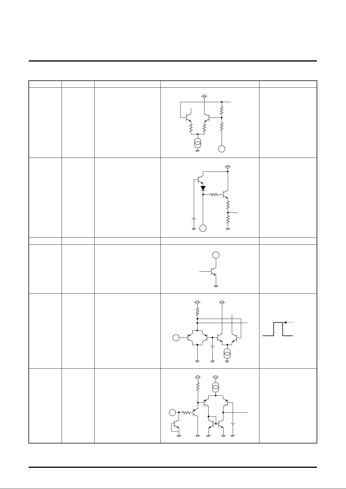
DESCRIPTION OF PIN
Pin No. Name DC voltage (V ) Peripheral circuit of pins Description of function
1 OSD BLK IN -
2
6
11
INPUT (R)
INPUT (G)
INPUT (B)
2.5
R
G
1
2K
B
0.37mA
2k
2.7V
0.37mA
2k
•Input pulses
•Connected to GND if not
used.
•Clamped to about 2.5V
due to clamp pulses
from pin 19.
•Input at low impedance.
3.7 to 5V
GND to1.7V
12
13
10
14
22
33
2.5V
0.3mA
3
8
VCC1 (R)
VCC1 (G)
12 -
VCC1 (B)
CP
•Apply equivalent
voltage to 3 channels.
•Input pulses
4
9
OSD IN (R)
OSD IN (G)
-
OSD IN (B)
1k
2k
3.7 to 5V
GND to 1.7V
•Connected to GND if not
0.5mA
5
GND 1 (R)
2.7V
used.
GND 1 (G)
GND 1 (B)
GND GND (5V)
GND 2
•SYNC ON GREEN
input pin for sync
separation.
7
7
INPUT
(S on G)
When open≈ 2.5V
500
Sync is negative.
input signal at Pin7,
3.33V
compare with the
reference voltage of
internal circuit in order to
separate sync signal.
•When not used, set to
0.22mA
0.15mA
0.22mA
OPEN.
18
MITSUBISHI ICs (Monitor)
PRELIMINARY
Notice:This is not a final specification.
Some parametric limits are subject to change.
BUS CONTROLLED 3-CHANNEL VIDEO PREAMP FOR CRT DISPLAY MONITOR
M52742ASP
DESCRIPTION OF PIN (cont.)
Pin No. Name DC voltage (V ) Peripheral circuit of pins Description of function
2.5V
•ABL (Automatic Beam
Limiter) input pin.
Recommended voltage
range is 0 to 5V.
When ABL function is not
used, set to 5V.
•Uniformity input pin.
Recommended
amplitude range is 0 to
5VP-P.
15 ABL IN When open 2.5V
16 Uniformity IN 5.75
1.2k
0.5mA
1.2k
20k
30k
15
200
20k
7.25V
16
17 VCC (5V) 5 -
18
19
S on G Sep
OUT
Clamp Pulse
IN
-
41k
-
19
2.2V
50k
5k
18
•Sync signal output pin,
Being of open collector
output type.
•Input pulses
2.5 to 5V
GND to 0.5V
•Input at low impedance.
0.15mA
20 SCL -
19
•SCL of I2C BUS
(Serial clock line)
20
2k
3V
VTH=2.3V

MITSUBISHI ICs (Monitor)
PRELIMINARY
Notice:This is not a final specification.
Some parametric limits are subject to change.
BUS CONTROLLED 3-CHANNEL VIDEO PREAMP FOR CRT DISPLAY MONITOR
M52742ASP
DESCRIPTION OF PIN (cont.)
Pin No. Name DC voltage (V ) Peripheral circuit of pins Description of function
50k
2
C BUS
21 SDA -
23
24
25
26
D/A OUT -
•SDA of I
(Serial data line)
21
2k
3V
VTH=2.3V
•D/A output pin.
Output voltage range is
0 to 5V, Min input current
is 0.18mA when D / A
output pin is 1V.
Max output current is
1.0mA.
27
28
31
34
29
32
35
Retrace BLK
IN
EXT Feed
Back (B)
EXT Feed
Back (G)
EXT Feed
Back (R)
OUTPUT (B)
OUTPUT (G)
OUTPUT (R)
-
Variable
Variable
50k
27
35k
36
50
50
R
G
B
2.25V
•Input pulses
2.5 to 5V
GND to 0.5V
•Connected to GND if not
used.
•A resistor is needed on
the GND side.
Set discretionally to
maximum 15mA,
depending on the
required driving capacity.
36 VCC2
12
•Used to supply power to
output emitter follower
only.
20

MITSUBISHI ICs (Monitor)
PRELIMINARY
Notice:This is not a final specification.
Some parametric limits are subject to change.
BUS CONTROLLED 3-CHANNEL VIDEO PREAMP FOR CRT DISPLAY MONITOR
M52742ASP
DESCRIPTION OF PIN (cont.)
Pin No. Name DC voltage (V ) Peripheral circuit of pins Description of function
35k
30
Main
Brightness
-
APPLICATION METHOD FOR M52742SP
CLAMP PULSE INPUT
Clamp pulse width is recommended
above 15kHz, 1.0µsec
above 30kHz, 0.5µsec
above 64kHz, 0.3µsec.
The clamp pulse circuit in ordinary set is a long round about way,
and beside high voltage, sometimes connected to external terminal,
it is very easy affected by large surge.
Therefore, the Fig. shown right is recommended.
30
NOTICE OF APPLICATION
•Make the nearest distance between output pin and pull down
resistor.
•Recommended pedestal voltage of IC output signal is 2V.
•It is recommended that
the IC be used between
pedestal voltage 2V and
3V.
19
EXT-FEED BACK
In case of application circuit example of lower figure, Set up R1, R2
which seems that the black level of the signal feedbacked from
Power AMP is 1V, when the bottom of output signal is 1V.
MAIN BRIGHTNESS
DC:1 to 5V
Pre Amp
INPUT R
M52742ASP
R OUT PUT
Black level 1 to 5V
R Feed back
Black level 1 to 5V
Power Amp
Power Amp OUT
R1
R2
21
EXT-FEED BACK APPLICATION CIRCUIT
 Loading...