

21
MITSUBISHI<LINEAR IC>
TENTATIVE
DESCRIPTION
RECOMMENDED OPERATING CONDITIONS
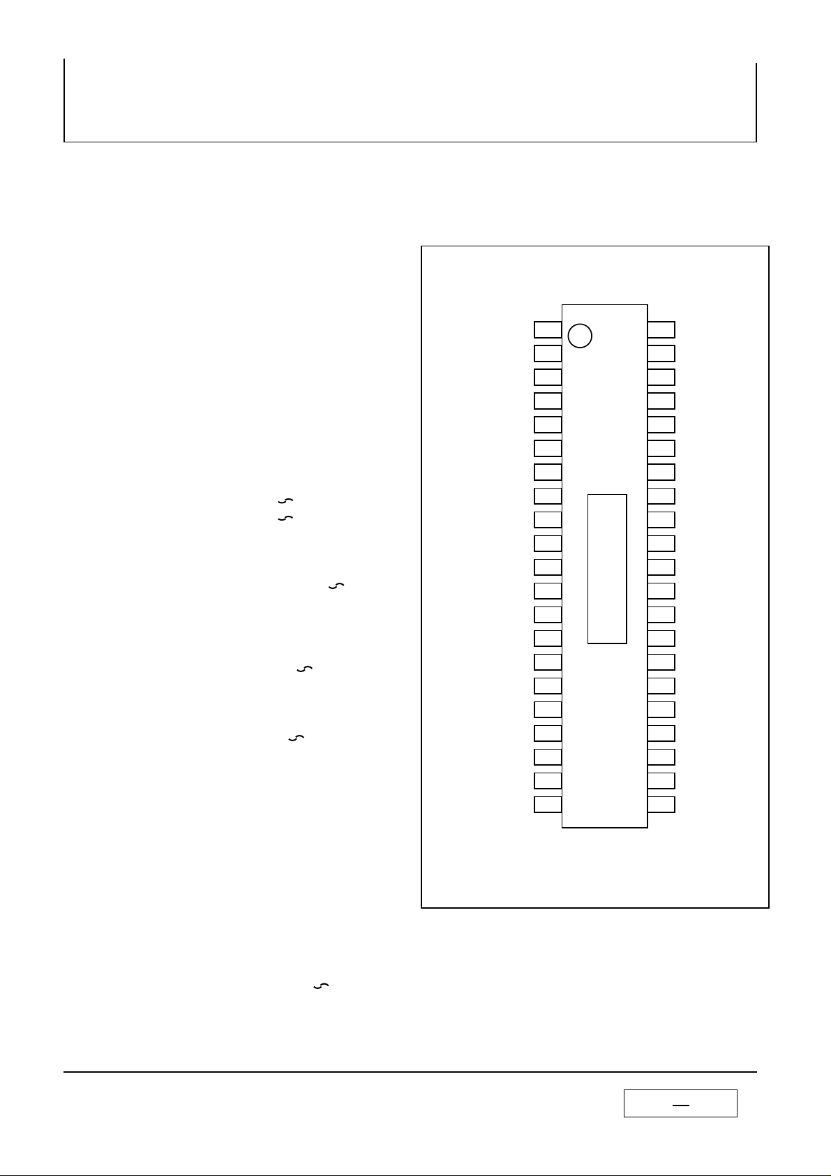
Outline:42P9R-B
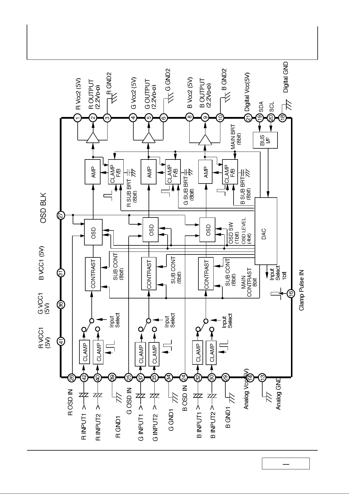
OSD BLK IN
R INPUT1
R VCC1
R OSD IN
R GND 1
G INPUT1
G OSD IN
B VCC1
B OSD IN
Digital VCC
R VCC2
Digital GND
SDA
SCL
Clamp Pulse IN
GND
1
GND
GND
R INPUT2
G INPUT2
B INPUT2
R OUTPUT
R GND2
G VCC2
G OUTPUT
G GND2
B VCC2
B OUTPUT
B GND2
GND
Analog Vcc
GND
GND
GND
GND1GND
GND
FEATURES
M52739FP
IIC BUS controled 3channel video pre-amplifier for LCD display monitor.
M52739FP is integrated Circuit for LCD Display Monitor.It
is controlled IIC BUS and Band Wide is 180MHz.
It includes OSD Blanking ,OSD Mixing,Wide Band
Amplifier,Main/Sub Contrast Main/Sub Brightness
,and 2 Input routes.
Vcc Voltage is 5V and Flat package is used.
then it is the suitable to LCD monitor.
1.Frequency :
Band Width
2.Input :
3.Output :
4.Contrast :
5.Brightness :
6.OSD Adjust :
RGB 180MHz(at -3dB)
OSD 80MHz
RGB Input D range:Max1VP-P positive
2 input routes is changed by IIC BUS
RGB OSD 3.5VP-P 5.0VP-P(positive)
OSD BLK 3.5VP-P 5.0VP-P(positive)
RGB 2.2VP-P (Max)
OSD 2.0VP-P (Max)
Output dynamic range 0.5 3.0V
It can drive 14pF
Both of sub and main contrast
are controlled by IIC Bus(8bit).
Control Range :-15dB +15dB.
Both of sub and main contrast
are controlled by IIC Bus(8bit).
Control Range :0.5V 3.0V.
2 Control Ranges (Max1VP-P or Max2VP-P )
are able to be changed by IIC Bus.
PIN CONFIGURATION
2
3
4
5
6
7
8
9
10
11
12
Analog Gnd
13
14
15
16
17
18
19
20
21
42
41
40
39
38
37
36
35
34
33
32
31
30
29
28
27
26
25
24
23
22
G VCC1
G GND 1
B INPUT1
B GND 1
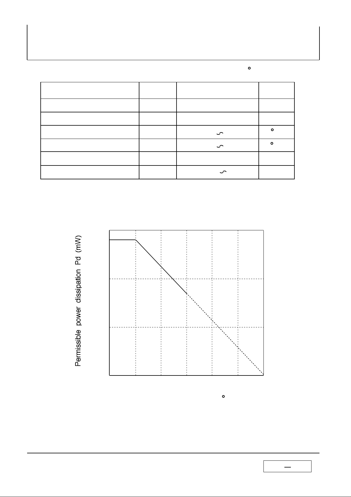
Supply Voltage Range 4.7V 5.3V
Rated Supply Voltage 5.0V
Consumption of electricity 800mW
MITSUBISHI
IIC BUS controled 3channel video pre-amplifier for LCD display monitor.
21
TENTATIVE
2
Block Diagram
MITSUBISHI<LINEAR IC>
M52739FP
MITSUBISHI
21
MITSUBISHI<LINEAR IC>
TENTATIVE
Vcc
Pd
Topr
Tstg
Vopr
Vopr'
6.0
1700
-40 +150
5.0
4.7 5.3
V
mW
C
3
0
Parameter
Symbol
Rating
Unit
Supply voltage
Ambient temperature
Storage temperature
Power dissipation
Ambient temperature Ta( C)
CVV
M52739FP
IIC BUS controled 3channel video pre-amplifier for LCD display monitor.
Absolute Maximum Rating (Ambient temperature: 25 C)
-20 +75
Recommended supply
voltage range
Thermal Derating Curve
3.0
2.8
2.0
1.0
1.68
25 50 75 100 125
MITSUBISHI
150
IIC BUS controled 3channel video pre-amplifier for LCD display monitor.
21
TENTATIVE
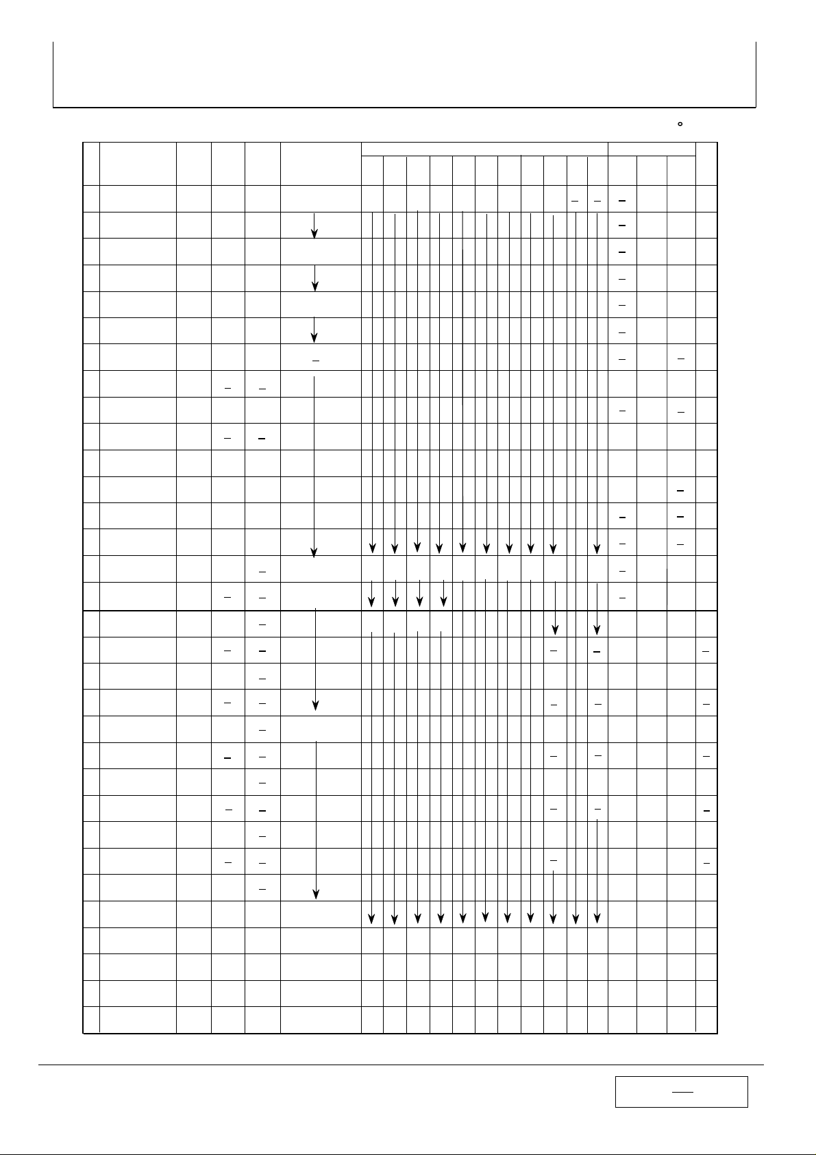
NO.
function
bit
sub
Data Byte
add.D7D6D5D4D3D2D1D0D7D6D5D4D3D2D1R/W
10001000=88H
M52739FP
Main contrast
8
01H
A07
A06
A05
A04
A03
A02
A01
A00010000002Sub contrast R
8
02H
A17
A16
A15
A14
A13
A12
A11
A10100000003Sub contrast G
8
03H
A27
A26
A25
A24
A23
A22
A21
A20100000004Sub contrast B
8
04H
A37
A36
A35
A34
A33
A32
A31
A3000000005
OSD level
4
05H606H707H808H909H
00H-------A9000000000
Main bright
Sub bright R
Sub bright G
Sub bright B
8888A47
A46
A45
A44
A43
A42
A41
A401000000A57
A56
A55
A54
A53
A52
A51
A5010000000
A67
A66
A65
A64
A63
A62
A61
A6010000000
A77
A76
A75
A74
A73
A72
A71
A7010000000----
A83
A82
A81
A800000000INPUT SW
101100
4
OSD SW
1
0AH-------AA000000000
(1) Slave address:
BUS CONTROL TABLE
(2) Each function's sub address:
MITSUBISHI<LINEAR IC>
M52739FP
11
1
MITSUBISHI
IIC BUS controled 3channel video pre-amplifier for LCD display monitor.
21
TENTATIVE
SDA
SCL
SPS
5
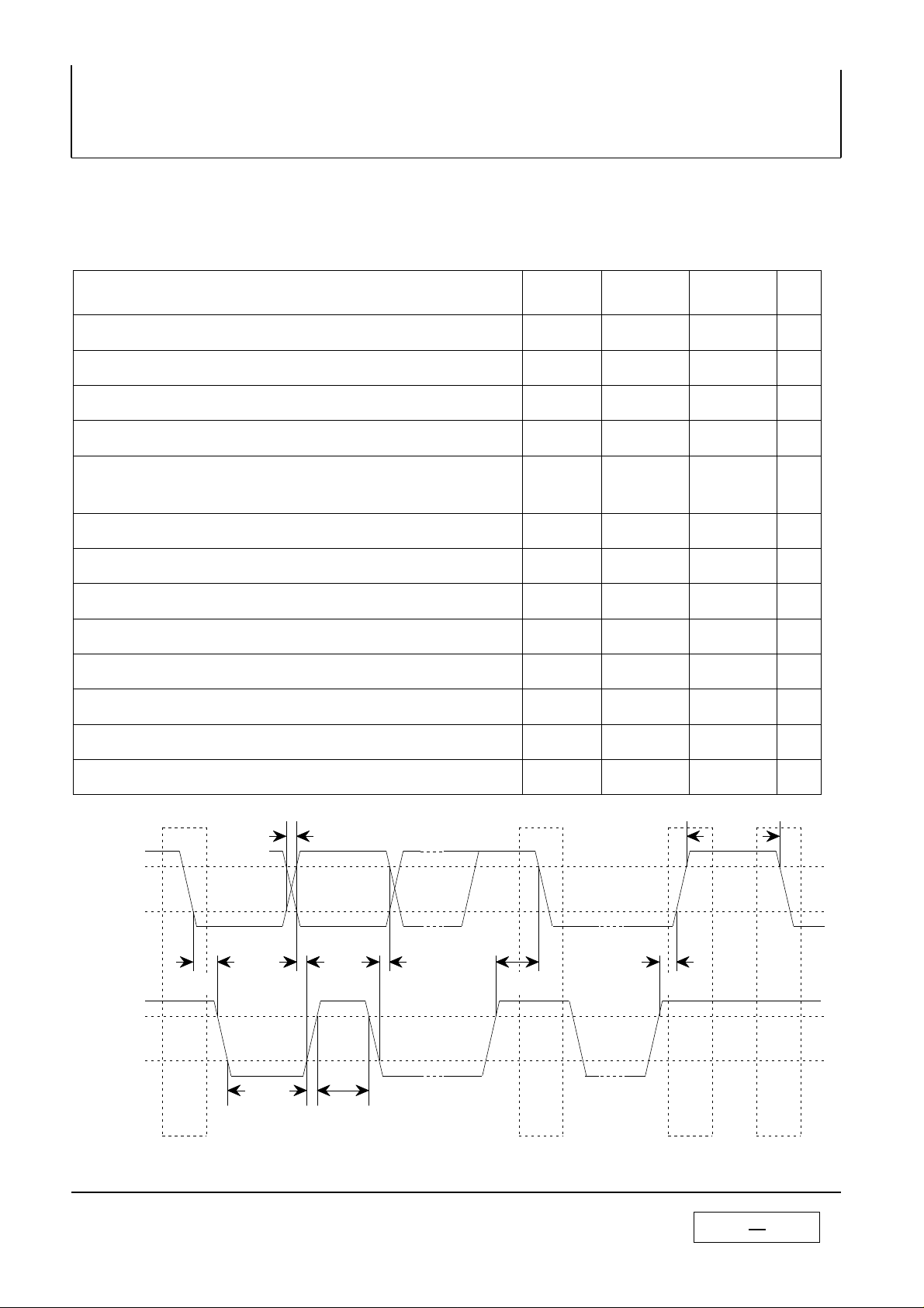
SDA,SCL CHARACTERISTICS
MIN
2
I C BUS CONTROL SECTION
MITSUBISHI<LINEAR IC>
M52739FP
parameter
min. input LOW voltage.
max. input HIGH voltage.
SCL clock frequency.
Time the bus must be free before a new transmission can start.
Hold time start condition.After this period the first clock pulse
is generated.
The LOW period of the clock.
The HIGH period of the clock.
Srt up time for start condition. (Only relevant for a repeated
start condition.)
Hold time DATA.
Set-up time DATA.
Rise time of both SDA and SCL lines.
symbol
VIL
VIH
fSCL
tBUF
tHD:STA
tLOW
tHIGH
tSU:STA
tHD:DAT
tSU:DAT
tR
MAX
-0.5 1.5 V
3.0
0 100 KHz
4.7
4.0
4.7
4.0
4.7
0
250
-
5.5 V
-
-
-
-
-
-
-
1000
unit
us
us
us
us
us
us
ns
ns
Fall time of both SDA and SCL lines.
Set-up time for stop condition.
tR, tF
VIL
VIH
tHD:STA
tSU:DAT
VIL
VIH
tLOW
S
tHIGH
tHD:DAT
tF
tSU:STO
-
4.0
tSU:STA tSU:STO
300
tBUF
ns
-
us
MITSUBISHI

TYP
MAX
MITSUBISHI
21
Symbol
Point
M52739FP
IIC BUS controlled 3channel video pre-amplifier for LCD display monitor.
TENTATIVE
6
Variable
Variable
SW(32,37,42)=a
Variable
Variable
Variable
Variable
If SW connect is not designated RGB Input SW :
SW(30,35,40)=a(b) SW(32,37,42)=b (a),SW(2,5,9,16,19,20,23,24,25,26,27)= a
No
parameter
Circuit current1
1
dynamic range
2
3
4
Maximum gain
5
6
Main contrast control
characteristics 1
7
Main contrast control
characteristics 2
8
Main contrast control
characteristics 3
9
Sub contrast control
characteristics 1
10
Sub contrast control
characteristics 2
11
Sub contrast control
characteristics 3
12
Main/sub contrast
control characteristics
13
Main brightness control
14
characteristics 1
Main brightness control
characteristics 2
15
Main brightness control
16
characteristics 3
Sub brightness control
17
characteristics 1
Sub brightness control
18
characteristics 2
Sub brightness control
19
characteristics 3
Frequency
characteristics 1
20
(50MHz-2Vpp)
Frequency relative
21
characteristics 1
(180MHz-2Vpp)
Frequency
characteristics 2
22
(50MHz-2Vpp)
Frequency relative
23
characteristics 2
(50MHz-2Vpp)
Frequency
24
characteristics 3
(180MHz-1Vpp)
Frequency relative
characteristics 3
25
(180MHz-1Vpp)
Frequency
characteristics 4
26
(180MHz-2Vpp)
Frequency relative
characteristics 4
27
(180MHz-2Vpp)
Crosstalk 1
28
Crosstalk 1'
29
Crosstalk 2
30
Crosstalk 2'
31
Output
Maximum
input1
Maximum
input2
Relative
maximum
gain
input1 - 2
50MHz-1
input1 - 2
50MHz-1
input1 - 2
50MHz-2
input1 - 2
50MHz-2
Icc1
Vomax
Vimax1
Vimax2
Gv
Gv
VC1
VC2
VC3
VSC1
VSC2
VSC3
VMSC
VB1
VB2
VB3
VSB1
VSB2
VSB3
FC1 OUT
∆FC1
FC2
∆FC2
FC3
∆FC3
FC4
∆FC4
OUT(2)
INCT1
OUT(5)
OUT(9)
INCT1'
OUT(5)
OUT(9)
OUT(2)
INCT2
OUT(5)
OUT(9)
INCT2'
OUT(9)
Test
IA
OUT
IN
OUT
IN
OUT
OUT
OUT
OUT
OUT
OUT
OUT
OUT
OUT
OUT
OUT
OUT
OUT
OUT
OUT
OUT
OUT
OUT
OUT(2)
OUT(2)
OUT(5)
RGB
Input
Signal
SG2
SG2
Amplitude
SG2
Amplitude
Variable
SG1
SG1
SG1
SG1
SG1
SG1
SG1
SG1
SG3
SG3
SG3
SG3
SW(42)=b,Other SW=a
SW(37)=b,Other SW=a
SG3
SW(32)=b,Other SW=a
SG3
SG3
SG3
SW Connect
Supply Voltage
RGBInput SW
=a(ALL)
SW(30,35,40)=b
RGBInput SW
=a(ALL)
SW(2,5,9)=b
SW(40)=b,Other SW=a
SW(35)=b,Other SW=a
SW(30)=b,Other SW=a
01H
00H
Sub
Main
cont
cont
1
A6H
A6H
166
166
7FH
7FH
127
127
FFH
FFH
255
255
C8H
7FH
200
127
64H
100
14H
20
C8H
7FH
200
127
64H
100
14H2014H2014H
A6H
A6H
166
166
A6H
A6H
166
166
A6H
166
37H
55
A6H
166
02H 03H
Sub
cont
2
A6H
A6H
166
7FH
7FH
127
127
FFH
255
7FH
127
C8H
200
64H
100
A6H
A6H
166
A6H
166
166
7FH
127
C8H
64H
100
166
A6H
BUS CTL ( H )
Sub
cont
3
FFH
255
200
20
166
04H
05H 06H 07H
Main
Sub
brt
brt1
00H
00H
0
40H
7FH
64
127
FFH
255
7FH
127
00H
0
FFH
7FH
255
127
7FH
127
00H
40H
7FH
64
127
0
0
Sub
brt2
00H
00H
0
7FH
7FH
127
FFH
FFH
255
255
7FH
127
00H000H
7FH
127
Sub
brt3
127
7FH
127
7FH
127
MITSUBISHI<LINEAR IC>
Vcc=5V Ta=25 C
08H
09H
0AH
INPUT
OSD
Adj
00H
0
0
00H
OSD
SW
SW
0
0
00H
0
01H
1
MIN
2.2
1.0
1.0
12.0
0.8
7.1
2.7
0.2
7.1
2.7
0.2
1.7
2.2
1.3
0.3
1.8
1.3
0.8
-3.0
-1.0
-3.0
-1.0
-1.0
-1.0
-3.0
-1.0
Standard
100
15.0 18.0
1.0 1.2
8.6 10.1
4.2
0.4
8.6 10.1
4.2
0.4
2.0
2.5
1.5
0.5 0.7
2.0
1.5
1.0
0
0
3.0
0
0
0
3.0
0
-50
-30
-50
-30
130
5.7
0.6
5.7
0.6
2.3
2.8
1.7
2.2
1.7
1.2
3.0
1.0
5.0
1.0
1.0
1.0
5.0
1.0
-40
-20
-40
-20
Unit
mA
Vp-p
Vp-p
Vp-p
dB
dB
dB
Vp-p
dB
dB
Vp-p
Vp-p
V
V
V
V
V
V
dB
dB
dB
dB
dB
dB
dB
dB
dB
dB
dB
dB
TYP
MAX
MITSUBISHI
21
Symbol
Point
M52739FP
IIC BUS controlled 3channel video pre-amplifier for LCD display monitor.
TENTATIVE
7
ns
If SW connect is not designated RGB Input SW :
SW(30,35,40)=a(b) SW(32,37,42)=b (a),SW(2,5,9,16,19,20,23,24,25,26,27)= a
No
parameter
Crosstalk 1
between RGB ch
32
50MHz-1
Crosstalk 1'
between RGB ch
33
180MHz-1
Crosstalk 2
between RGB ch
34
50MHz-2
Crosstalk 2'
between RGB ch
35
180MHz-2
Crosstalk 3
between RGB ch
36
50MHz-3
Crosstalk 3'
between RGB ch
37
50MHz-3
characteristics
38
pulse characteristics
39
characteristics
40
Relative pulse
characteristics
41
Clamp pulse
42
threshold voltage
Clamp pulse
43
minimum width
OSD input threshold
44
OSD BLK input
45
threshold voltage
OSD Pulse
46
characteristics Tr
OSD Pulse
47
characteristics Tf
OSD adjust control
48
characteristics 1
OSD adjust control
49
relative characteristics 1
OSD adjust control
50
characteristics 2
OSD adjust control
51
characteristics 2
OSD adjust control
52
characteristics 3
OSD adjust control
53
characteristics 3
OSD adjust control
54
characteristics 4
OSD adjust control
55
characteristics 4
OSD BLK
56
characteristics
OSD BLK
57
characteristics
OSD input threshold
58
OSD BLK input
59
threshold voltage
Pulse
Tr1
Relative
Pulse
Tr2
Tr2
voltage
relative
relative
relative
relative
voltage
RGB
Test
Input
Signal
CHCT1
OUT
CHCT1'
OUT
CHCT2
OUT
CHCT2'
OUT
OUT
CHCT3
OUT
CHCT3'
Tr1
OUT
Tr1
∆Tr1
OUT
Tf2
∆Tf2
VthCP
OUT
WCP
OUT
PDCH
OUT
PDCL
OUT
OUT
OTr1
OTf2
Oaj1
OUT
∆Oaj1
Oaj2 OUT
∆Oaj2
Oaj3
OUT
∆Oaj3
Oaj4
OUT
∆Oaj4
OUT
OBLK
∆OBLK
VthOSD
OUT
OUT
VthBLK
SW Connect
Supply Voltage
SW(42)=b,OtherSW=a
SG3
SG3
SW(37)=b,OtherSW=a
SG3
SG3
SW(32)=b,OtherSW=a
SG3
SG3
SG1
SG1
SG1
SG1
SG1
SG1
SW(24,25,
SW(24,25,26,27)=b
SW(27)=b
SG1
26,27)=b
00H
Main
cont
A6H
166
00H
A6H
166
01H
Sub
cont
1
A6H
166
00H
0
0
A6H
166
02H 03H
Sub
cont
2
A6H
A6H
166
166
00H000H
A6H
166
BUS CTL ( H )
Sub
cont
3
0
A6H
166
04H
05H 06H 07H
Main
Sub
brt
brt1
40H
7FH
64
127
40H
7FH
64
127
Sub
brt2
7FH
127
7FH
127
Sub
brt3
7FH
127
7FH
127
08H
OSD
Adj
00H
0FH
01H
0FH
15
01H
00H
MITSUBISHI<LINEAR IC>
Vcc=5V Ta=25 C
09H
0AH
INPUT
OSD
SW
SW
0
00H
15
00H
1
01H
01H
1
0
Standard
MIN
-0.8
-0.8 -0.8
1.5 2.0
0.2
0
1.7
0.8
0.7
0
0.8
0.7
1
0.8
0.3
1
0.8
0.0
-0.15
2.0
2.0
-25
-20
-15
-10
-25
-20
-15 -10
-25 -20
-15
-10
1.7
0.0
-0.8
1.7
0.0
0.5
0.0
0.0
3.0
6.0
3.0
6.0
2.0
2.3
1.0
1.2
1.0
1.3
1.0
1.2
1.0
1.3
1.0
1.2
0.5
0.7
1.0
1.2
0.0
0.2
0.0
0.15
2.5
3.0
3.0
2.5
2.5
Unit
dB
dB
dB
dB
dB
dB
nS
nS
nS
nS
V
uS
V
V
ns
Vp-p
Vp-p
Vp-p
Vp-p
Vp-p
V
V

TYP
MAX
MITSUBISHI
21
Symbol
Point
M52739FP
IIC BUS controlled 3channel video pre-amplifier for LCD display monitor.
TENTATIVE
8
V19=5V
V20=5V
VOSD=5V
V27=5V
mAnAuA
V16=0V
V19=0V
V20=0V
VOSD=0V
V27=0V
mAmAmA
uA
V16=5V
uA
If SW connect is not designated RGB Input SW :
SW(30,35,40)=a(b) SW(32,37,42)=b (a),SW(2,5,9,16,19,20,23,24,25,26,27)= a
No
60
61
62
63
64
Pin20
65
Input Current L
Pin24 25 26
66
Input Current H
Pin24 25 26
67
Input Current L
68
Pin27
69
Input Current L
parameter
Pin16
Input Current H
Pin16
Input Current L
Pin19
Input Current H
Pin19
Input Current L
Pin20
Input Current H
Pin27
Input Current H
I16H
I16L
I19H
I19L
I20H
I20L
IOSDH
IOSDL
I27H
I27L
Test
I16
I16
I19
I19
I20
I20
I24
I25
I26
I24
I25
I26
I27
I27
RGB
Input
Signal
SW Connect
Supply Voltage
SW(16)=b
SW(16)=b
SW(19)=b
SW(19)=b
SW(20)=b
SW(20)=b
SW(24,25,26)=b
SW(24,25,26)=b
SW(27)=b
SW(27)=b
00H
Main
cont
01H
Sub
cont
1
02H 03H
Sub
cont
2
BUS CTL ( H )
Sub
cont
3
04H
05H 06H 07H
Main
Sub
brt
brt1
Sub
brt2
Sub
brt3
08H
OSD
Adj
MITSUBISHI<LINEAR IC>
Vcc=5V Ta=25 C
09H
INPUT
SW
0AH
OSD
SW
Standard
MIN
-0.7
0.7
0
40
0
0.7
-1.3
1.5
-1.3
1.5
Unit
nA
mA

21
MITSUBISHI<LINEAR IC>
TENTATIVE
9
1)
2)
the amplitude of the input signal when the output signal starts becoming distorted.
GV = VOUT(2) / VOUT(5), VOUT(5) / VOUT(9), VOUT(9) / VOUT(2)
VOUT
0.7
GV = 20 LOG
(dB)
VOUT(2,5,9).Maximum gain GV is calculated by the equation below:
VOUT
0.7
VC1=20 LOG
(dB)
Measuring condition and procedure are the same as described in Note7.
3)5)6)7)8)9)10)
11)
12)
Measured with a current meter at test point IA.
Waveform output
0.0
(V)
VOH
VOL
4)
13)
Measuring condition and procedure are the same as described in Note7.
Measuring condition and procedure are the same as described in Note7.
Measuring condition and procedure are the same as described in Note7.
Measuring condition and procedure are the same as described in Note7.
Measuring condition and procedure are the same as described in Note7.
M52739FP
IIC BUS controled 3channel video pre-amplifier for LCD display monitor.
Measuring conditions are as listed in supplementary Table.
Decrease Main Brt or Sub Brt gradually, and measure the voltage when the bottom of waveform
output is distorted. The voltage is called VOL.
Next, increase V30 gradually, and measure the voltage when the top of waveform output is
distorted. The voltage is called VOH.Voltagr Vomax is calculated by the equation below:
Vomax =VOH-VOL
Increase the input signal(SG2) at Input1 amplitude gradually, starting from 700mVp-p. Measure
Increase the input signal(SG2) at Input2 amplitude gradually, starting from 700mVp-p. Measure
the amplitude of the input signal when the output signal starts becoming distorted.
Input SG1, and read the amplitude output at OUT(2,5,9). The amplitude is called
Relative maximum gain GV is calculated by the equation below:
Measuring the amplitude output at OUT(2,5,9). The measured value is called VOUT(2,5,9).
MITSUBISHI

21
TENTATIVE
14)
17)
18)
15)
16)
19)
20)
21)
22)
23)
24)
Measure the DC voltage output at OUT(2,5,9). The measured value is called VB1.
25)
26)
27)
same
way, measure the output amplitude when SG3 to 50MHz is as input signal.The
measured value is called VOUT(2,5,9).
Frequency characteristics FC1(2,5,9) is calculated by the equation below:
between the channels.
Measuring condition and procedure are the same as described in Note33,expect SG3 to
same as described in Note33
between the channels.
Measuring condition and procedure are the same as described in Note14.
Measuring condition and procedure are the same as described in Note14.
Measuring condition and procedure are the same as described in Note14.
Measuring condition and procedure are the same as described in Note14.
Measuring condition and procedure are the same as described in Note14.
VOUT Vp-p
FC1=20 LOG
(dB)
output amplitude when inputed SG3(1MHz) : 4.0Vp-p
MITSUBISHI<LINEAR IC>
M52739FP
IIC BUS controled 3channel video pre-amplifier for LCD display monitor.
First, SG3 to 1MHz is as input signal.
Control the main contrast in order that the amplitude of sine wave output is 2.0Vp-
p.Control the brightness in order that the bottom of sine wave output is 1.0V.By the
Relative characteristics ∆FC1 is calculated by the difference in the output
Relative characteristics ∆FC2 is calculated by the difference in the output
between the channels.
SG3 to 1MHz is as input signal. Control the main contrast in order that the amplitude of sine
wave output is 1.0Vp-p.By the same way, measure the output amplitude when SG3 to
180MHz is as input signal.
Relative characteristics ∆FC3 is calculated by the difference in the output
Change OUT SW from a to b .Measuring condition and procedure are the
Relative characteristics ∆FC4 is calculated by the difference in the output
between the channels.
MITSUBISHI
10

21
MITSUBISHI<LINEAR IC>
TENTATIVE
11
VOUT(5,9)
CHCT1= 20 LOG
(dB)
VOUT(2)
Measuring condition and procedure are the same as described in Note32,expect SG3 to 180MHz.
the equation below:
VOUT(2,9)
CHCT2= 20 LOG
(dB)
VOUT(5)
Measuring condition and procedure are the same as described in Note34,expect SG3 to 180MHz.
the equation below:
VOUT(2,5)
CHCT3= 20 LOG
(dB)
VOUT(9)
Measuring condition and procedure are the same as described in Note36,expect SG3 to 180MHz.
32)
34)
36)
37)
33)
35)
VOUT(2)'
INCT1= 20 LOG
(dB)
VOUT(2)
Measuring condition and procedure are the same as described in Note28,expect SG3 to 180MHz.
28)
29)
and calculate crosstalk
VOUT(2)'
INCT2= 20 LOG
(dB)
VOUT(2)
30)
31)
and calculate crosstalk.
M52739FP
IIC BUS controled 3channel video pre-amplifier for LCD display monitor.
Input SG3 (50MHz) to pin42 only, set Input SW of IIC BUS to 0 and then measure the
waveform amplitude output at OUT(2).The measured value is called VOUT(2).On equal
terms set Input SW of IIC BUS to 1.And then measure the waveform amplitude output at
OUT(2)'.Crosstalk INCT1 is calculated by the equation below:
Similarly measure the waveform amplitude output at
OUT(5) when signal input only Pin37 and OUT(9)when signal input only Pin32
Input SG3 (50MHz) to pin40 only, set Input SW of IIC BUS to 1 and then measure the
waveform amplitude output at OUT(2).The measured value is called VOUT(2).On equal
terms set Input SW of IIC BUS to 0.And then measure the waveform amplitude output at
OUT(2)'.Crosstalk INCT2 is calculated by the equation below:
Similarly measure the waveform amplitude output at
OUT(5) when signal input only Pin35 and OUT(9)when signal input only Pin30
Measuring condition and procedure are the same as described in Note30,expect SG3 to 180MHz.
Input SG3 (50MHz) to pin42 only, and then measure the waveform amplitude output at
OUT(2,5,9).The measured value is called VOUT(2,5,9).Crosstalk CHCT1 is calculated by
the equation below:
Input SG3 (50MHz) to pin37 only, and then measure the waveform amplitude output at
OUT(2,5,9).The measured value is called VOUT(2,5,9).Crosstalk CHCT2 is calculated by
Input SG3 (50MHz) to pin32 only, and then measure the waveform amplitude output at
OUT(2,5,9).The measured value is called VOUT(2,5,9).Crosstalk CHCT3 is calculated by
MITSUBISHI

21
MITSUBISHI<LINEAR IC>
TENTATIVE
12
TR = (Tr2) - (Tr1) (nsec)
90%0%10%
Tr2
Tf2
38)
40)
pulse width (a point of 1.5V) when the output pedestal voltage turn decrease with unstable.
equation below:
42)
43)
44)
45)
PDC3.Pedestal voltage temperature characteristics 2 is calculated by the equation below:
Tr =VOUT(2) - VOUT(5) , VOUT(5) - VOUT(9) , VOUT(9) - VOUT(2)
Tf = VOUT(2) - VOUT(5) , VOUT(5) - VOUT(9) , VOUT(9) - VOUT(2)
41)
TF = (Tf2) - (Tf1) (nsec)
M52739FP
IIC BUS controled 3channel video pre-amplifier for LCD display monitor.
Control the contrast in order that the amplitude of output signal is 2.0Vp-p.
Control the brightness in order that the Black level of output signal is 1.0V.
Measure the time needed for the input pulse to rise from 10 % to 90 % (Tr1) and for the
output pulse to rise from 10 % to 90 % (Tr2) with an active prove.
Pulse characteristics TR is calculated by the equations below :
2 2
39)
Relative Pulse characteristics1 Tr is calculated by the equation below:
Measure the time needed for the input pulseto fall from 90 % to 10 % (Tf1) and for the
output pulse to fall from 90 % to 10 % (Tf2) with an active prove.
Pulse characteristics TF is calculated by the equations below :
2 2
Relative Pulse characteristics2 Tf is calculated by the equation below:
100%
Tr1
or
Turn down the SG4 input level gradually from 5.0Vp-p, monitoring the waveform
output.Measure the top level of input pulse when the output pedestal voltage turn
decrease with unstable.
Decrease the SG4 pulse width gradually from 0.5us, monitoring the output. Measure the SG4
Tf1
or
Measure the pedestal voltage at 25 C. The measured value is called PDC1.
Measure the pedestal voltage at temperature of - 20 C. The measured value is
called PDC2.Pedestal voltage temperature characteristics 1 is calculated by the
Measure the pedestal voltage at temperature of 75 C. The measured value is called
MITSUBISHI

21
MITSUBISHI<LINEAR IC>
TENTATIVE
13
Measure the time needed for the output pulse to fall from 90% to 10% (OTF) with an active prove.
47)
Measure the time needed for the output pulse to rise from 10% to 90% (OTR) with an active prove.
46)
and is treated as Oaj1.
Oaj1 = VOUT(2) / VOUT(5), VOUT(5) / VOUT(9), VOUT(9) / VOUT(2)
Relative characteristics Oaj1 is calculated by the equation below:
48)
49)
Measuring condition and procedure are the same as described in Note48.
Measuring condition and procedure are the same as described in Note49.
50)
51)
56)
57)
the output reaches 0V. The measured value is called VthOSD.
the blanking period is disappeared. The measured value is called VthBLK.
58)
59)
52)
53)
54)
55)
Supply 5V to V16,and then measure input current into Pin16
Supply 0V to V16,and then measure input current into Pin16
60)
61)
62)
63)
64)
65)
66)
67)
68)
69)
Measuring condition and procedure are the same as described in Note48.
Measuring condition and procedure are the same as described in Note48.
Measuring condition and procedure are the same as described in Note49.
Measuring condition and procedure are the same as described in Note49.
Supply 5V to V19,and then measure input current into Pin19
Supply 0V to V19,and then measure input current into Pin19
Supply 5V to V20,and then measure input current into Pin20
Supply 0V to V20,and then measure input current into Pin20
Supply 5V to V(24,25,26)and then measure input current into Pin(24,25,26)
Supply 0V to V(24,25,26)and then measure input current into Pin(24,25,26)
Supply 5V to V27,and then measure input current into Pin27
Supply 0V to V27,and then measure input current into Pin27
M52739FP
IIC BUS controled 3channel video pre-amplifier for LCD display monitor.
Measure the amplitude output at OUT(2,5,9). The measured value is called VOUT(2,5,9),
Measuring the amplitude output at OUT(2,5,9). The measured value is called OBLK.
Relative OSD BLK characteristics OBLK is calculated by the equation below:
OBLK = VOUT(2) / VOUT(5), VOUT(5) / VOUT(9), VOUT(9) / VOUT(2)
Reduce the SG5 input level gradually, monitoring output.Measure the SG5 level when
Confirm that output signal is being blanked by the SG5 at the time.
Monitoring to output signal, decreasing the level of SG5. Measure the top level of SG6 when
MITSUBISHI

21
MITSUBISHI<LINEAR IC>
TENTATIVE
(75%)
SG2
SG3
SG4
SG5
8us
33us
0.5us
5us
are variable.
Amplitude is partially variable
14
Amplitude is partially variable
M52739FP
IIC BUS controled 3channel video pre-amplifier for LCD display monitor.
SG No.
SG1
Video signal
(all white)
Video signal
(step wave)
Sine wave
(for freq. char.)
INPUT SIGNAL
Pulse with amplitude of
0.7Vp-p (f=30KHz).
Video width of 25us.
0.7VP-P
0.7VP-P
Sine wave amplitude of
0.7Vp-p.
f=1MHz,50MHz,150MHz
(variable)
Clamp
pulse
OSD pulse
fH=30KHz
5VTTL
5VTTL
Pulse width
and amplitude
MITSUBISHI

21
MITSUBISHI<LINEAR IC>
TENTATIVE
15
10pF1K10pF1K10pF
1K
M52739FP
IIC BUS controled 3channel video pre-amplifier for LCD display monitor.
TEST CIRCUIT
SW27
SW26
SW25
SW24
MITSUBISHI

IIC BUS controled 3channel video pre-amplifier for LCD display monitor.
21
TENTATIVE
Input0.7Vp-p
FFH
2
00H
FFH
1
OSD SW:1
2
3
7FH
Input0.7Vp-p
FFH
Main Contrast FFH
023
7FH24
00H
FFH
00H
4
00H
FFH
00H
Electrical Characteristics
Main Contrast Control Characteristics
MITSUBISHI<LINEAR IC>
M52739FP
Sub Contrast Control Characteristics
2.2V
Sub Contrast FFH
1
0
00H
Main Contrast Control Data
00H
2.2V
1
00H
00H
Main Contrast Control Data
Main Brightness Control Characteristics Sub Brightness Control Characteristics
3
3
Main Brightness FFH
Sub Brightness FFH
7FH
2
7FH
0.5V
1
0
Main Brightness Control Data
OSD Adjust Control Characteristics
0
OSD Adjust Control Data
1
0.5V
0
Sub Brightness Control Data
OSD SW:0
MITSUBISHI
16

21
MITSUBISHI<LINEAR IC>
TENTATIVE
clamp pulses by the outside circuit.
17
M52739FP
IIC BUS controled 3channel video pre-amplifier for LCD display monitor.
Application Method
CLAMP PULSE INPUT
Clamp pulse width is recommended
above 15 KHz, 1.0 usec
above 30 KHz, 0.5 usec
above 64 KHz, 0.3 usec
The clamp pulse circuit in ordinary set is a long round about way,
and beside high voltage, sometimes connected to external terminal,
it is very easy affected by large surge.
Therefore, the Fig. shown right is recommended.
16
Notice of application
1.Recommended pedestal voltage of IC output signal is 1V.
2.This IC has 2 Input routes. When the 2 Input signal input at different timing,clamp pulses
which synchronize with selected signals is needed. In this case,it is necessary to change
MITSUBISHI

IIC BUS controled 3channel video pre-amplifier for LCD display monitor.
21
TENTATIVE
M52739FP
75
47uF
SCL
SDA
OSD BLK IN
G OSD IN
5VTTL
5VTTL
5VTTL
5VTTL
75
INPUT1
3.3uF75757575
INPUT2
INPUT1
INPUT1
1k1K1K
1K
18
47uF
47uF
47uF
47uF
3.3uF
3.3uF
3.3uF
3.3uF
3.3uF
47uF
47uF
47uF
APPLICATION EXAMPLE
MITSUBISHI<LINEAR IC>
M52739FP
42
R
41
G
INPUT2
B
INPUT2
R OSD IN
B OSD IN
37383940
36
2223242526272829303132333435
5V
1 2 3 4 5 6 7 8 9 10 11 12
R OUTPUT
G OUTPUT
B OUTPUT
Condenser:0.01uF(unless otherwise specified.)
14 15 16 17 18 19 20 21
13
Clamp
Pulse IN
MITSUBISHI

IIC BUS controled 3channel video pre-amplifier for LCD display monitor.
21
TENTATIVE
8
5
1314Analog Gnd
Analog Vcc
516Clamp Pulse In
20mA
19
GND
GND
Terminal Description
Name
DC
Voltage
(V)
MITSUBISHI<LINEAR IC>
M52739FP
peripheral Circuit
Remark
1
4
2
5
9
3
R VCC 2
G VCC 2
B VCC2
OUTPUT (R)
2
OUTPUT (G)
OUTPUT (B)
R GND 2
10
6
G GND 2
B GND 2
21K
16
1K
2.0V
2.0V
0.2mA
more than 200nSec
2.5 5V
0.5V GND
Input at low impedance.
MITSUBISHI

21
MITSUBISHI<LINEAR IC>
TENTATIVE
1921SDA3V192K50K
VTH=2.3V
VTH=2.3V
SCL3V202K50K18Digital Vcc
5V
Digital GND
20
GND
24
B OSD IN
G OSD IN
R OSD IN
M52739FP
IIC BUS controled 3channel video pre-amplifier for LCD display monitor.
DC
Name
Voltage
(V)
peripheral Circuit
Remark
SDA for II C
(Serial data line)
24
25
26
SCL for II C
(Serial clock line)
20
Input pulses
3.5 5V
1.0V GND
1k
1k
2.5V
2.5V
MITSUBISHI

21
MITSUBISHI<LINEAR IC>
TENTATIVE
34
39
5
G GND 1
R GND 1
37
42
G INPUT 1
R INPUT 1
7111517283338
NC
radiation of heat
30
21
GND500 (off) 3.5V(on)
322
OSD BLK IN
27
Input pulses
Connected to GND if
not used.
M52739FP
IIC BUS controled 3channel video pre-amplifier for LCD display monitor.
No.
27
29
30
32
35
Name
B GND 1
B INPUT 2
B INPUT 1
G INPUT 2
DC
Voltage
(V)
2.1 V
peripheral Circuit
1k
2.5V
2K 2K
Remark
3.5 5V
1.0V GND
330
2.5V
1.5mA
Clamped to about 2.1 V
due to clamp pulses
from pin16.
Input at low impedance.
40
31
36
41
12
2
R INPUT 2
R VCC 1
G VCC 1
B VCC 1
2.0V
CP
0.3mA
Connect GND for
MITSUBISHI
 Loading...