MITSUBISHI ICs (Monitor)
PRELIMINARY
Notice:This is not a final specification.
Some parametric limits are subject to change.
3-CHANNEL VIDEO PREAMPLIFIER WITH OSD MIXING, RETRACE BLANKING
DESCRIPTION
The M52738P is semiconductor integrated circuit for CRT display
monitor.
It includes OSD blanking function, OSD mixing, Wide-band
amplifier, Main and sub contrast controls, Brightness control
function.
FEATURES
Frequency Band Width :RGB............................130MHz (at -3dB)
•
Input :RGB.............................................................0.7V
OSD.......................................1.6V
OSD BLK...............................1.6V
Retrace BLK........................1.2V
Output :RGB...............................................................4V
OSD...............................................................4V
•
Contrast and brightness can be controlled with a main control.
The Main control changes contrast or brightness of 3-channels
simultaneously. The sub control changes contrast of each
channel independently.
OSD.............................................80MHz
(typ.)
P-P
minimum (positive)
P-P
minimum (positive)
maximum (negative)
P-P
P-P
P-P
P-P
(min.)
(min.)
M52738P
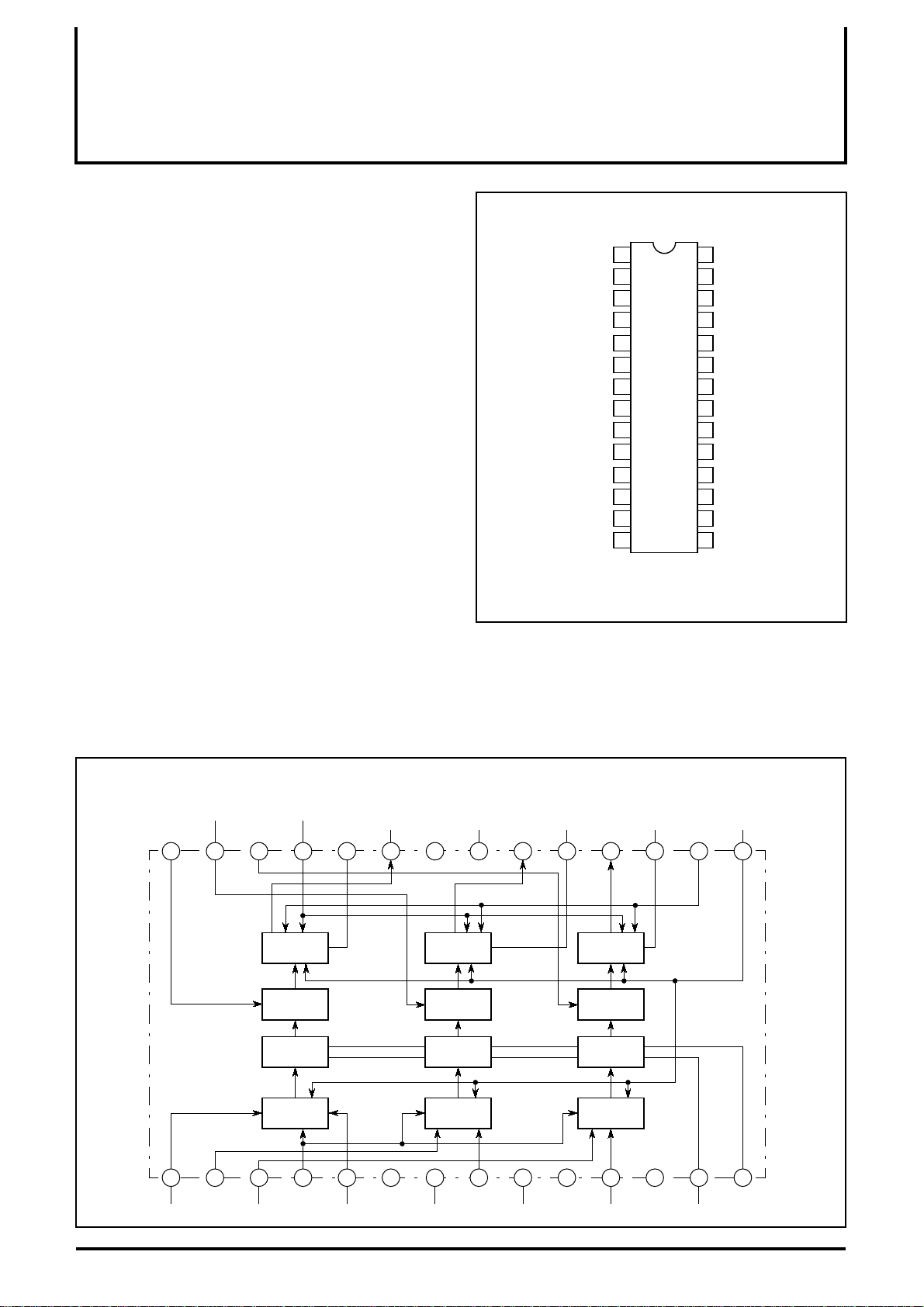
PIN CONFIGURATION (TOP VIEW)
OSD IN (R) SUB CONTRAST (R)
OSD IN (G)
OSD IN (B)
OSD BLK IN
INPUT (R)
INPUT (G)
INPUT (B)
MAIN CONTRAST
OSD ADJ
1
2
3
4
5
CC1
V
6
GND
7
8
VCC1
9
GND
10
11
REF
V
12
13
14 15
28
27
26
25
24
M52738P
23
22
21
20
19
18
17
16
SUB CONTRAST (G)
SUB CONTRAST (B)
BRIGHTNESS
HOLD (R)
OUTPUT (R)
V
GND
OUTPUT (G)
HOLD (G)
OUTPUT (B)
HOLD (B)
BLK IN
CP IN
CC2
STRUCTURE
Bipolar silicon monolithic IC
APPLICATION
CRT display monitor
RECOMMENDED OPERATING CONDITION
Supply voltage range....................................................11.4 to 12.6V
Rated supply voltage................................................................12.0V
BLOCK DIAGRAM
SUB
CONTRAST (G)
SUB
CONTRAST (R)
28 2627 25 24 2021 19 1718 16 1523 22
CONTRAST (B)
BRIGHTNESS
SUB
R AMP
R SUB
CONTRAST
OUTPUT (R)
HOLD (R) V
CC2
CONTRAST
G AMP
G SUB
GND
OUTPUT (G)
HOLD (G)
OUTPUT (B)
Outline 28P4
B AMP
B SUB
CONTRAST
HOLD (B)
BLK IN
CP IN
R
CONTRAST
R
OSD MIX
13245 98101211 13 1467
CC1OSD BLK IN
OSD IN (G) GNDINPUT (G)
OSD IN (R)
OSD IN (B)
V
G
CONTRAST
G
OSD MIX
GND
B
CONTRAST
B
OSD MIX
REF
V
CC1INPUT (R)
INPUT (B)
MAIN CONTRAST
OSD ADJV
1

°
°
±
−
∆
MITSUBISHI ICs (Monitor)
PRELIMINARY
Notice:This is not a final specification.
Some parametric limits are subject to change.
3-CHANNEL VIDEO PREAMPLIFIER WITH OSD MIXING, RETRACE BLANKING
ABSOLUTE MAXIMUM RATINGS
Symbol Parameter Ratings Unit
V
CC
P
d
T
opr
T
stg
V
opr
V
opr’
Surge Electrostatic discharge
ELECTRICAL CHARACTERISTICS
Symbol Parameter
CC
I
Gmax Maximum gain
Gmax Relative maximum gain
CR1
V
CR2
V
V
SCR1
SCR2
V
V
B1
B2
V
B3
V
C1
F
C2
F
Tr Video output rise time
Tf Video output fall time
thCP
V
OT
r
OT
f
O
aj1
O
aj2
OSD
BLK
H
H
vth
Note1: The ambient temperature is 25 ° C.
2: The supply voltage is 12V.
3: The direction of a current that flows toward the IC is regarded as plus.
Supply voltage 13 V
Power dissipation 2000 mW
Operating temperature -20 to 70
Storage temperature -40 to 150
Recommended operating supply voltage 12 V
Recommended operating supply voltage range
11.4 to 12.6 V
200 V
(Ta=25 ° C, V
CC1
=V
CC2
=12V, unless otherwise noted)
Test
point
I
CC
6, 9, 21
No input. Measurement of current
that flows into 6, 9 and 21
18, 20, 2318, 20, 23 input VSG, 15 input PG
V13=4V V26, V27, V28=4V
−−
Contrast control characteristics
(typical)
Contrast control characteristics
(minimum)
Sub contrast control characteristics
(typical)
Sub contrast control characteristics
(minimum)
Brightness control characteristics
(maximum)
Brightness control characteristics
(typical)
Brightness control characteristics
(minimum)
Frequency characteristics 1
(f=50MHz;maximum)
Frequency characteristics 2
(f=130MHz; maximum)
Clamp pulse threshold voltage
OSD output rise time
OSD output fall time
OSD adjust control (maximum)
OSD adjust control (minimum)
OSD input threshold voltage
th
Retrace BLK characteristics
Retrace BLK input threshold voltage
18, 20,
18, 20,
18, 20,
18, 20,
18, 20,
18, 20,
18, 20,
18, 20,
18, 20,
18, 20,
18, 20,
18, 20,
18, 20,
18, 20,
18, 20,
18, 20,
18, 20,
18, 20,
18, 20,
18, 20, 23 input VSG, 15 input PG
V13=2V V26, V27, V28=4V
23
18, 20, 23 input VSG, 15 input PG
V13=0.25V V26, V27, V28=4V
23
18, 20, 23 input VSG, 15 input PG
V26, V27, V28=2V V13=4V
23
18, 20, 23 input VSG, 15 input PG
V26, V27, V28=0.25V V13=4V
23
15 input PG
23
V25=10V
15 input PG
23
V25=1V
15 input PG
23
V25=0V
18, 20, 23 input SG 0 dB
23
18, 20, 23 input SG -3
23
18, 20, 23 input PG, 15 input PG 3.0 nsec
23
18, 20, 23 input PG, 15 input PG 4.0 nsec
23
18, 20, 23 input VSG, 15 input PG 1.2 V
23
1, 2, 3 input PG, 15 input PG 4 nsec
23
1, 2, 3 input PG, 15 input PG 10 nsec
23
1, 2, 3 input PG, 15 input PG
23
V14=4V V26, V27, V28=2V
1, 2, 3 input PG, 15 input PG
23
V14=0V V26, V27, V28=2V
1, 2, 3 input PG, 15 input PG
23
4 input PG
16 input PG
23
16 input PG 1.2 V
23
Test conditions
M52738P
C
C
Limits
Min. Typ. Max.
100 mA
20 dB
0.8 1.0 1.2 dB
14 dB
0.25 V
15.5 dB
1.1 V
8.5 V
1.1 V
−−
0.1 V
−−
5 V
0 V
1.6 V
−−
0.5 V
Unit
P-P
P-P
dB
P-P
P-P
2
 Loading...