MITSUBISHI ICs (AV COMMON)
M52393P/FP
EDTV2 IDENTIFICATION SIGNAL DETECTOR
DESCRIPTION
The M52393 are integrated-circuits of a semiconductor, developed
especially for EDTV2 identification signal detection.
In contrast to such ICs, few products on the IC market had the
simple function of detecting identification signals. For that purpose,
many manufacturers had to combine discrete components (nonICs) with gate arrays. There was a great demand for ICs that
enabled cost reduction.
In order to satisfy demand, we have developed the EDTV2
identification signal processing ICs that include all necessary
capabilities for detection (synchronous signal separation, line
counter, filters, level detection, and bit judgment). The use of such
ICs reduces parts, eliminates the need for complicated adjustment,
and enables easy handling and cost reduction.
FEATURES
•
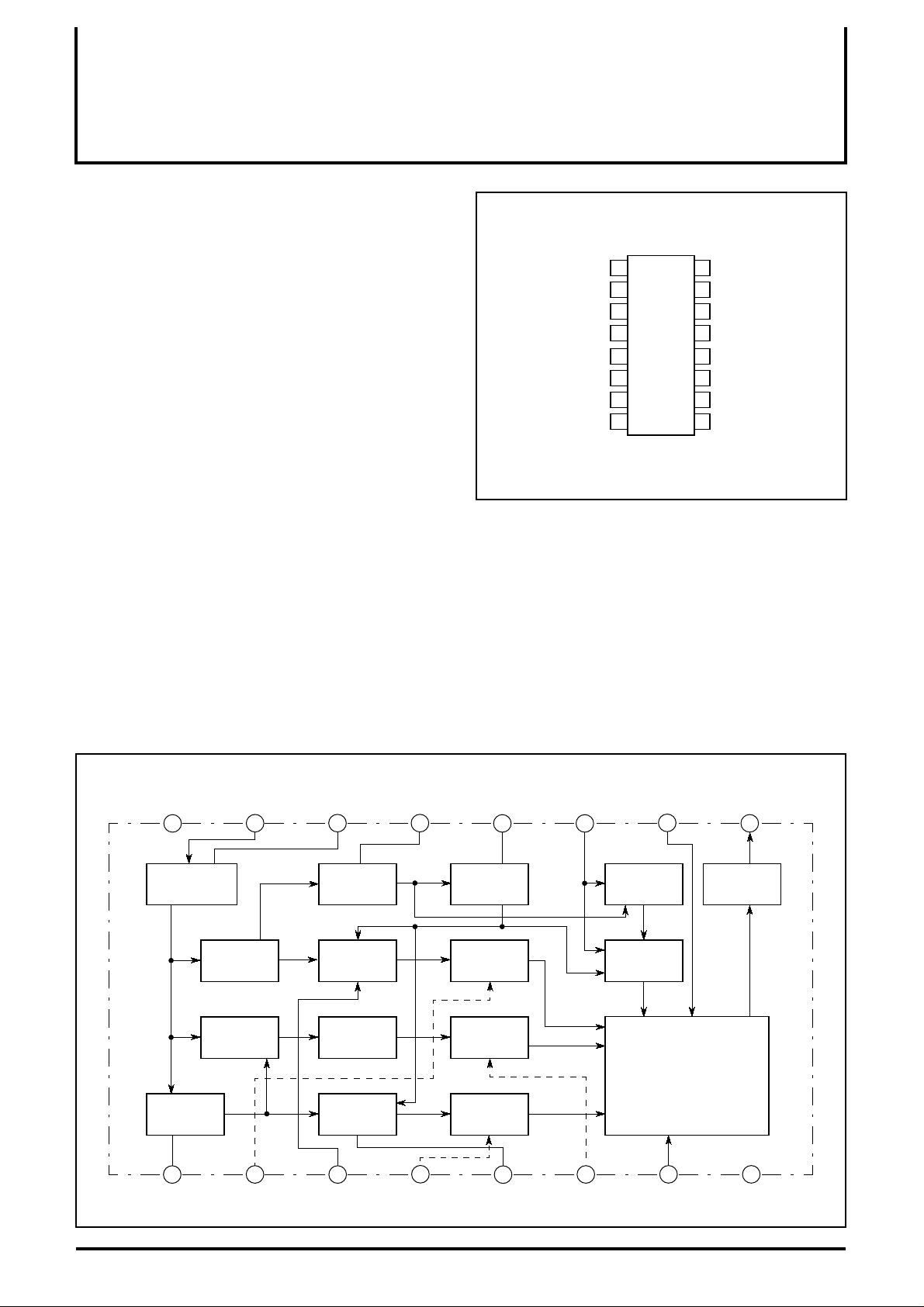
All necessary detection capabilities, such as a synchronous signal separation circuit, are integrated into a single microchip. The
use of the microchip can simplify application circuits, and eliminate the need for adjustment. (Only two inputs are provided:
video signal input and fsc signal input.)
•
Our original method is used for distinguishing EDTV2 identification signals from normal video signals.
Therefore the accuracy of identification is improved.
The detection level is adjustable.
•
The microchip operates on a single supply voltage of 5V.
•
Two types of packages are provided:
•
DIP with a lead pitch of 2.54mm (M52393P); and SOP with a
pitch of 1.27mm (M52393FP).
PIN CONFIGURATION (TOP VIEW)
2.04M TRAP
COMP1
CLAMP1
COMP2
CLAMP2
COMP3
CORRELATION SW
LINE
GND
1
2
3
4
7
8
16
V
15
M52393P/FP
VIDEO IN
14
3.58M TRAP
13
SYNC SEPA FILTER
125
V.SEPA FILTER
116
f
10
FRAME/FIELD SW
DET OUT
9
CC
SC IN
Outline 16P4
16P2N-A
APPLICATION
TV and videocassette recorder compatible with EDTV2.
RECOMMENDED OPERATING CONDITION
Supply voltage range........................................................4.7 to 5.3V
Rated supply voltage.....................................................................5V
BLOCK DIAGRAM
V
CC VIDEO IN V.SEPA FILTER
16
CLAMP
TRAP (3.58MHz)
14dB AMP
TRAP
(2.1M)
1
LPF 1
BPF
(2.1M)
Sync
Sepa.
DET 3
SYNC SEPA
1314
4
COMP2 COMP32.04M TRAP
12
V Sepa
COMP 1
COMP 3
COMP 2
fSC INFILTER
11
5
6
3.58M TRAP
15
CLAMP 1
CLAMP 2
2
3
FRAME/
FIELD SW
10
PULSE GEN.
Counter
Bit judge
LINE GNDCLAMP2CLAMP1COMP1
CORRELATION SW
DET OUT
9
LED
DRIVER
87
1

°
°
−
−
−
MITSUBISHI ICs (AV COMMON)
M52393P/FP
EDTV2 IDENTIFICATION SIGNAL DETECTOR
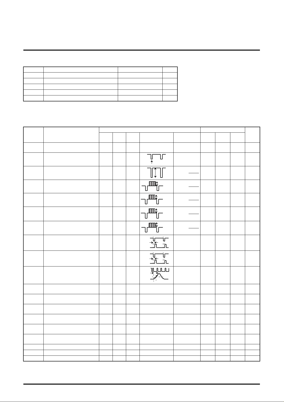
ABSOLUTE MAXIMUM RATINGS
(Ta=25 ° C, Measured on a standard board, unless otherwise noted)
Symbol Parameter Ratings Unit
V
CC
P
d
T
opr
T
stg
K
θ
( ) indicate FP values.
ELECTRICAL CHARACTERISTICS
Supply voltage 6 V
Power dissipation 1400 (980) mW
Operating temperature -20 to 75
Storage temperature -40 to 125
Thermal derating (Ta ≥ 25 ° C) 14 (9.8) mW/ ° C
(Ta=25 ° C, V
CC
=5.0V, unless otherwise noted)
SPECIFICATIONS
Test conditions Limits
Symbol Parameter
CC1
I
Circuit current1
V15 Clamp voltage
G1 14dB Amp gain
TRP1 TRAP gain1
TRP2 TRAP gain2
Input
Input
signal
SG15
SG110VF1
SG15
SG11S1F2
SG15
SG11S2F1
SG15
SG11T1F1
SG15
SG11T2F1
Output Output signal Remarks Min. Typ. Max.
16 DC Current 21 28 35 mA
AC15
AC1 12 14 16 dB
AC1 10.3 13.3 16.3 dB
AC1
1MHz
2.04MHz
C
C
Sync chip
voltage
G1=20log
T1=20log
T2=20log
M
286mV
M
143mV
M
143mV
Unit
2.2 2.5 2.8 V
-12.0 -6.0 dB
TRP3 TRAP gain3
TRP4 TRAP gain4
SSD Sync sepa. delay
SSM Sync sepa. delay at 30%
VSD V sepa. delay
VC1 CLAMP1 voltage
VC2 CLAMP2 voltage
LDI1 Driving capacity at Hi 1
LDI2 Driving capacity at Hi 2
HDI1 Driving capacity at Lo 1
HDI2 Driving capacity at Lo 2
SG15
SG11T3F1
SG15
SG11T4F1
SG15
SG11S1F1
SG15
SG11S3F1
SG15
SG11S1F1
SG15
SG11S1F3
SG15
SG11S1F3
SG15
SG11S1F1
SG15
SG11S1F1
SG15
SG11S1F1
SG15
SG11S1F1
AC1
AC1 4.7 10.7 16.7 dB
12 Delay 0.7 1.0 1.3 µ s
12
12 Delay 38 48 58 µ s
3.58MHz
5MHz
15
12
15
12
15
12
T3=20log
T4=20log
SSM=SSD-M
2.5V
3 DC Voltage 2.8 3.1 3.4 V
5 DC Voltage 2.8 3.1 3.4 V
9 DC Voltage 4.0 4.2 4.5 V
9 DC LDI2=LDI1-M 0 0.1 0.5 V
9 DC Voltage 0 0.1 0.5 V
9 DC HDI2=M-HDI1 0 0.2 0.5 V
Delay
M
143mV
M
143mV
-15.5 -9.5 dB
0
0.5 µ s
V2 COMP. 1 voltage SG11 F1 2 DC Voltage 2.2 2.5 2.8 V
V4 COMP. 2 voltage SG11 F1 4 DC Voltage 2.2 2.5 2.8 V
V6 COMP. 3 voltage SG11 F1 6 DC Voltage 2.2 2.5 2.8 V
2

EDTV2 IDENTIFICATION SIGNAL DETECTOR
TEST CONDITIONS
Symbol Parameter
I
CC1
Circuit current1 G G 5
1234567910111416
V15 Clamp voltage G G 5
G1 14dB Amp gain G G 5
TRP1 TRAP gain1 G G 5
TRP2 TRAP gain2 G G 5
TRP3 TRAP gain3 G G 5
TRP4 TRAP gain4 G G 5
SSD Sync sepa. delay G G 5
SSM Sync sepa. delay at 30% G G 5
VSD V sepa. delay G G 5
VC1 CLAMP1 voltage G G 5
VC2 CLAMP2 voltage G G 5
LDI1 Driving capacity at Hi 1
LDI2 Driving capacity at Hi 2
HDI1 Driving capacity at Lo 1
HDI2 Driving capacity at Lo 2
0.4 0.4 0.4 2.5
0.4 0.4 0.4 2.5
0.4 0.4 0.4
0.4 0.4
V2 COMP. 1 voltage G G 5
V4 COMP. 2 voltage G G 5
V6 COMP. 3 voltage G G 5
Supply voltage Switch condition
2.5
2.5
0.5 2.5
0.4 0.5 2.5
MITSUBISHI ICs (AV COMMON)
M52393P/FP
5
5
5
5
1-1 1-2
ON
ON
ON
ON
ON
ON
ON
ON
ON
ON
ON
ON
ON
ON
ON
ON
ON
ON
ON
357
aa
ON ON
aa
ON ON
aa
ON ON
ON ON
aa
aa
ON ON
aa
ON ON
ON ON
aa
ON ON
aa
aa
ON ON
aa
ON ON
ON ON
aa
aa
ON ON
aa
ON ON
ON ON
aa
ON ON
aa
aa
ON ON
aa
ON ON
ON ON
aa
aa
ON ON
9-1 9-2
11-1 11-2
10
a
ON
a
ON
a
ON
ON
a
a
ON
a
ON
ON
a
ON
a
a
ON
a
ON
ON
a
a
ON
a
ON
ON
b
ON
a
c
ON
a
ON
ON
a
a
ON
14-1 14-2 14-3
12
a
a
a
a
a
a
a
a
a
a
a
a
a
a
a
a
a
a
a
ON
ON
ON
ON
ON
ON
ON
ON
ON
ON
ON
ON
ON
ON
ON
ON
ON
ON
ON
3

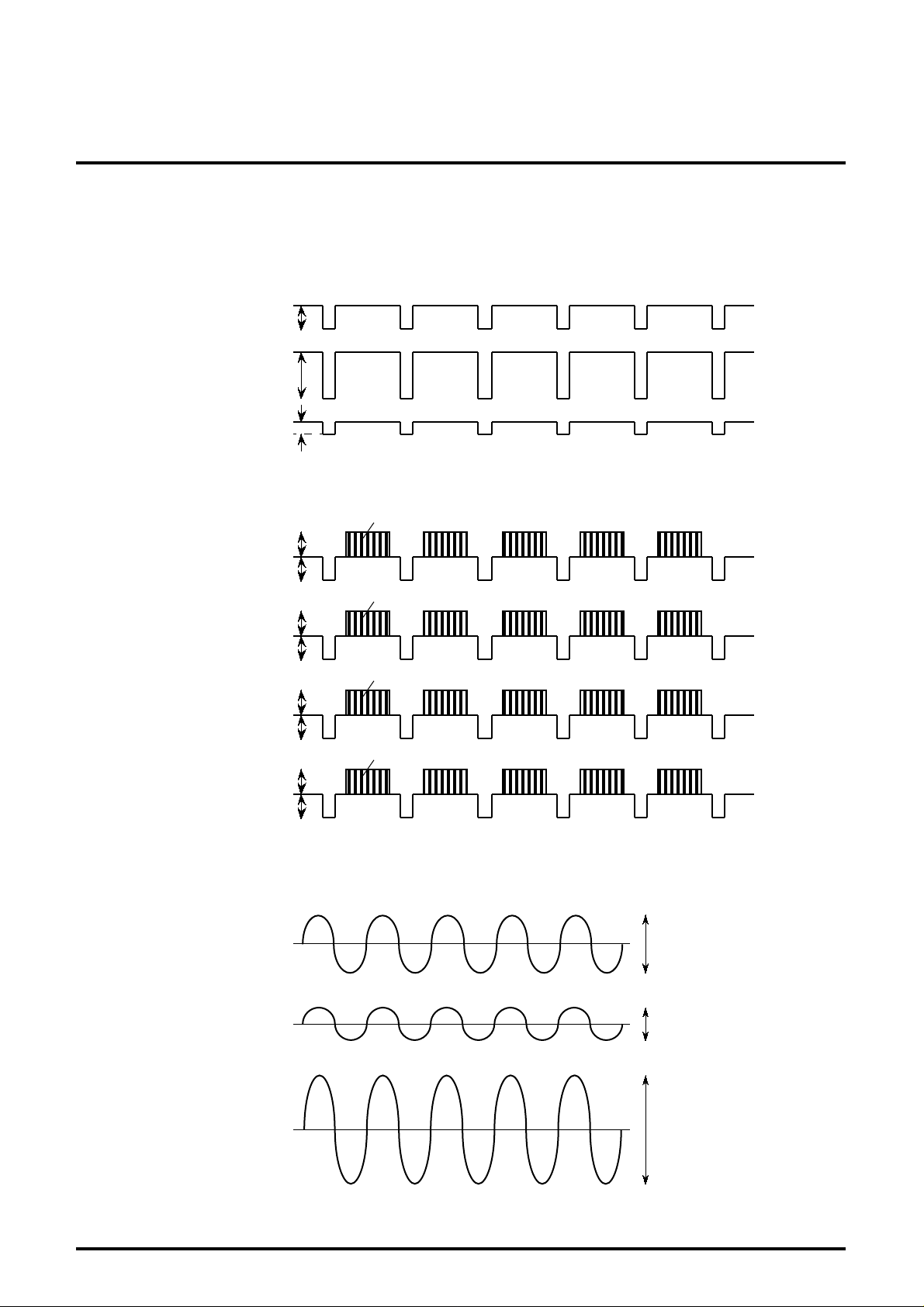
INPUT SIGNALS FOR TESTING
MITSUBISHI ICs (AV COMMON)
M52393P/FP
EDTV2 IDENTIFICATION SIGNAL DETECTOR
15pin input video signal (SG15)
S1 143mV
S2 286mVP-P
S3
T1
T2
T3
P-P
42mV
P-P
143mVP-P
143mVP-P
143mVP-P
143mVP-P
143mVP-P
143mVP-P
(Signals during V. Sync are not shown)
L20 L21 L22 L23 L24
1MHz
2.04MHz
3.58MHz
5MHz
T4
143mVP-P
143mVP-P
F1
F2
F3
3.58MHz
0
3.58MHz
0
3.58MHz
0
300mVP-P
100mV
P-P
600mVP-P
4

MITSUBISHI ICs (AV COMMON)
M52393P/FP
EDTV2 IDENTIFICATION SIGNAL DETECTOR
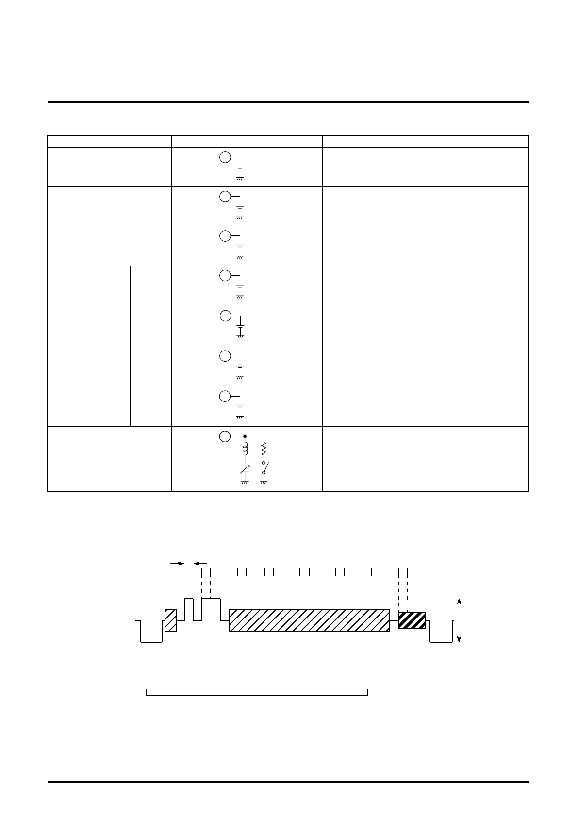
MODE T ABLE
Mode Conditions Functions
2
COMP. 1 OFF Detector off at Bit 1 to 5, 24
COMP. 2 OFF Detector off at Bit 25 to 27
COMP. 3 OFF 2.04MHz detector off at Bit 25 to 27
0 to 0.3V
4
0 to 0.3V
6
0 to 0.3V
ON
Line correlation SW
(Shown in Fig.1)
OFF
Frame
Frame/Field SW
(Shown in Fig.2)
Field
TRICK MODE
FUNCATIONAL DESCRIPTION
Input signal
7fsc
7
7
10
10
14
39µH
47pF
0 to 0.5V
2 to 3V
(2.5V at open)
0 to 0.5V
2 to 3V
(2.5V at open)
500Ω
ON
In a case an EDTV2 identification signal (or an equivarent
one) is detected a couple of times during three lines of 21
to 23 (line 284 to 286), the output will be Lo (a standard
signal).
On the other hand, the output will be Hi (an EDTV2 signal) through the ID signal is detected a couple of times
during the three lines.
The detection is performed once a field. The choice
between Odd or Even is difficult. (effective data : 8 fields/
8 frames)
The detection is performed in both fields. (effective data :
8 fields/4 frames )
The output state before the TRICK mode setting is kept
regardless of an input signal.
123456789101112131415161718192021222324252627Bit
Video in pin15
H.SYNC
Bit 1⋅2 3 4 5 24 25⋅26⋅27
Name Reference Letter box Parity SQZ 0 Sine wave for confirming
NRZ form
fsc in pin11 fsc, 0.3VP-P ±6dB, Sine wave (ansynchronous signals are permitted)
5
22H/285H
4/7fsc
286mV
P-P
(80/140IRE)
 Loading...