Mitsubishi M51995FP, M51995AP Datasheet
SWITCHING REGULATOR CONTROL
DESCRIPTION
M51995A is the primary switching regulator controller which is
especially designed to get the regulated DC voltage from AC power
supply.
This IC can directly drive the MOS-FET with fast rise and fast fall
output pulse.
Type M51995A has the functions of not only high frequency OSC
and fast output drive but also current limit with fast response and
high sensibility so the true "fast switching regulator" can be
realized.
It has another big feature of current protection to short and over
current,owing to the integrated timer-type protection circuit,if few
parts are added to the primary side.
The M51995A is equivalent to the M51977 with externally resettable OVP(over voltage protection)circuit.
MITSUBISHI (Dig./Ana. INTERFACE)
M51995AP/FP
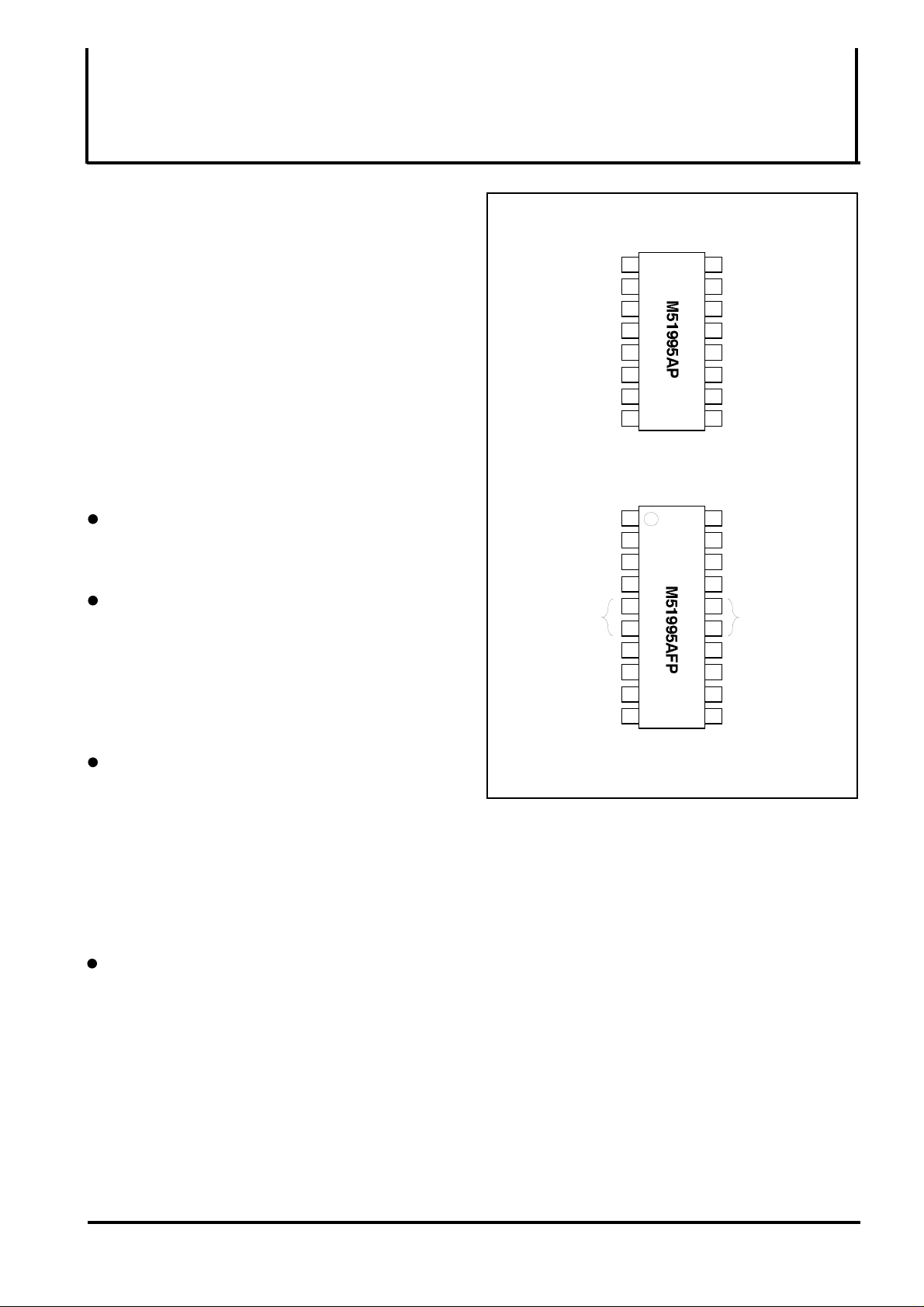
PIN CONFIGURATION (TOP VIEW)
Vcc
COLLECTOR
VOUT
EMITTER
VF
ON/OFF
OVP
DET
F/B
1
2
3
4
Outline 16P4
16
CLM+
15
14
CLM-
13
GND
125
CT
116
T-OFF
107
CF
98
T-ON
FEATURES
500kHz operation to MOS FET
•Output current...............................................................±2A
•Output rise time 60ns,fall time 40ns
•Modified totempole output method with small through current
Compact and light-weight power supply
•Small start-up current............................................90µA typ.
•Big difference between "start-up voltage" and "stop voltage"
makes the smoothing capacitor of the power input section small.
Start-up threshold 16V,stop voltage 10V
•Packages with high power dissipation are used to with-stand the
heat generated by the gate-drive current of MOS FET.
16-pin DIP,20-pin SOP 1.5W(at 25°C)
Simplified peripheral circuit with protection circuit and built-in
large-capacity totempole output
•High-speed current limiting circuit using pulse-by-pulse
method(Two system of CLM+pin,CLM-pin)
•Protection by intermittent operation of output over current......
..........................................................Timer protection circuit
•Over-voltage protection circuit with an externally re-settable
latch(OVP)
•Protection circuit for output miss action at low supply
voltage(UVLO)
High-performance and highly functional power supply
•Triangular wave oscillator for easy dead time setting
Vcc
20
CLM+
19
18
CLM-
17
GND
165
156
147
CT
138
T-OFF
12
CF
1110
T-ON
VOUT
VF
1
2
3
4
COLLECTOR
EMITTER
HEAT SINK PIN HEAT SINK PIN
ON/OFF
OVP
9
DET
F/B
Outline 20P2N-A
Connect the heat sink pin to GND.
APPLICATION
Feed forward regulator,fly-back regulator
RECOMMENDED OPERATING CONDITIONS
Supply voltage range............................................12 to 36V
Operating frequency.................................less than 500kHz
Oscillator frequency setting resistance
•T-ON pin resistance RON...........................10k to 75kΩ
•T-OFF pin resistance ROFF..........................2k to 30kΩ
( / 27 )
1
SWITCHING REGULATOR CONTROL
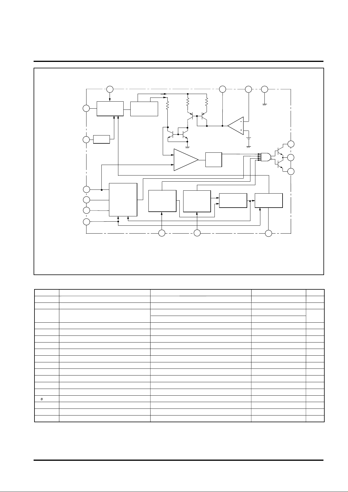
BLOCK DIAGRAM
OP AMP
ACTION
OSCILLATOR CAPACITANCE CF
ON/OFF
VCC
UNDER
VOLTAGE
LOCKOUT
VOLTAGE
REGULATOR
7.1V
5.8V
15.2K
1S
3K
MITSUBISHI (Dig./Ana. INTERFACE)
M51995AP/FP
F/B
500
6S
DET
GND
OVP(shut down)
OSCILLATOR RESISTANCE T-ON
(ON duty)
OSCILLATOR RESISTANCE T-OFF
(OFF duty)
VF
LATCH
OSCILLATOR
(TRIANGLE)
1S
+CURRENT
LIMIT LATCH
CLM+
+CURRENT LIMIT
1S
PWM
COMPARATOR
-CURRENT
LIMIT LATCH
-CURRENT LIMIT
CLM-
ABSOLUTE MAXIMUM RATINGS
Symbol Ratings UnitParameter Conditions
VCC Supply voltage
VC
IO
VVF
VON/OFF
VCLM-
VCLM+
IOVP
VDET
IDET
VFB
ITON
ITOFF
Pd
K
Topr
Tstg
Tj Junction temperature
Collector voltage
Output current
VF terminal voltage
ON/OFF terminal voltage
CLM-terminal voltage
CLM+terminal voltage
OVP terminal current
DET terminal voltage
DET terminal input current
F/B terminal voltage
T-ON terminal input current
T-OFF terminal input current
Power dissipation
Thermal derating factor
Operating temperature
Storage temperature
Peak
Continuous
Ta=25˚C
Ta>25˚C
PWM
LATCH
INTERMITTENT
ACTION AND
OSC CONTROL
INTERMITTENT OPERATION
2.5V
INTERMITTENT
CT
DETERMINE CAPACITANCE
36
36
±2
±0.15
Vcc
Vcc
-4.0 to +4.0
-0.3 to +4.0
8
6
5
0~10
-1
-2
1.5
12
-30 to +85
-40 to +125
150
COLLECTOR
VOUT
EMITTER
V
V
A
V
V
V
V
mA
V
mA
V
mA
mA
W
mW/˚C
˚C
˚C
˚C
Note 1."+" sign shows the direction of current flow into the IC and "-" sign shows the current flow from the IC.
2.This terminal has the constant voltage characteristic of 6 to 8V,when current is supplied from outside.The maximum allowable
voltage is 6V when the constant voltage is applied to this terminal.And maximum allowable current into this terminal is 5mA.
3.The low impedance voltage supply should not be applied to the OVP terminal.
( / 27 )
2
SWITCHING REGULATOR CONTROL
MITSUBISHI (Dig./Ana. INTERFACE)
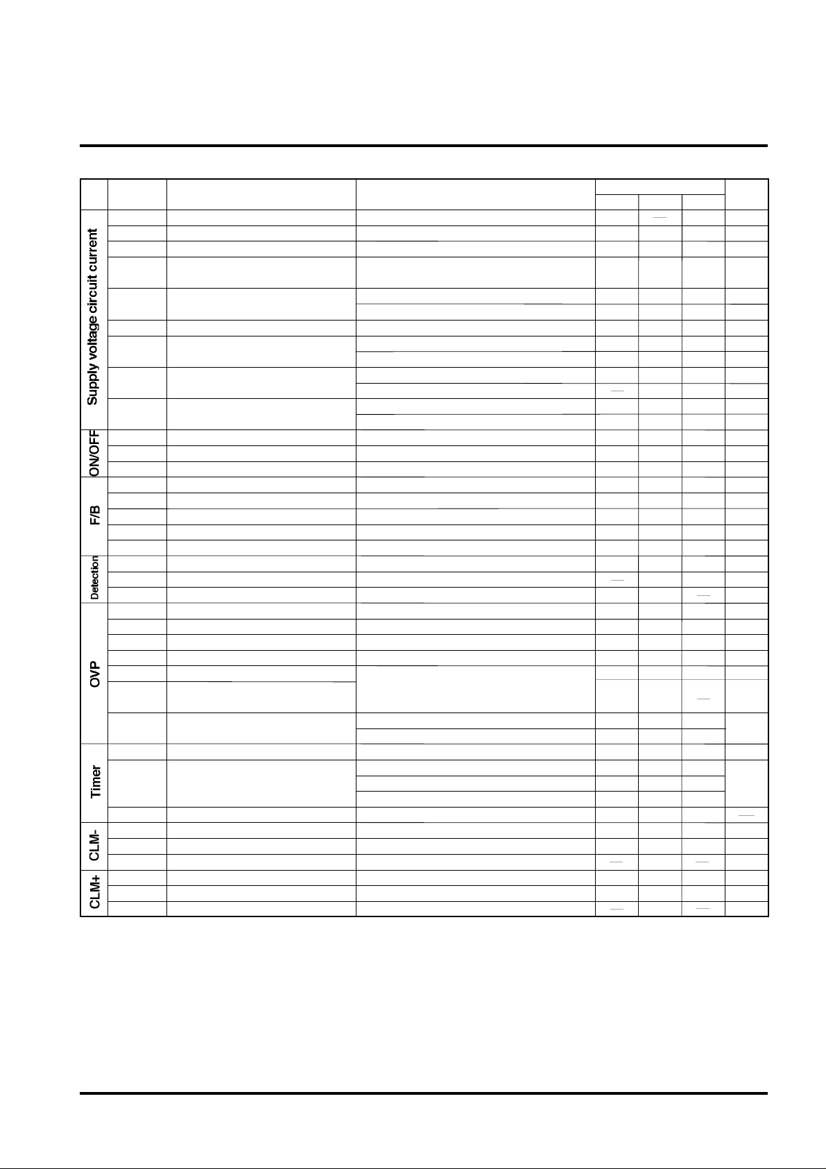
ELECTRICAL CHARACTERISTICS (VCC=18V, Ta=25°C, unless otherwise noted)
Block
Symbol Test conditions UnitParameter
VCC
VCC(START)
VCC(STOP)
∆Vcc
IccL
IccO
Icc OFF
Icc CT
Icc OVP
VTHH ON/OFF
VTHL ON/OFF
∆VTHON/OFF
IFBMIND
IFBMAXD
∆IFB
VFB
RFB
VDET
IINDET
GAVDET
VTHOVPH
∆VTHOVP
ITHOVP
IINOVP
VCCOVPC
VCC(STOP)
-VCCOVPC
ITHOVPC
fTIMER
ITIMECH
TIMEOFF/ON
VTHCLM-
IINCLM-
TPDCLM-
VTHCLM+
IINCLM+
TPDCLM+
Operating supply voltage range
Operation start up voltage
Operation stop voltage
Difference voltage between
operation start and stop
Stand-by current
Operating circuit current
Circuit current in OFF state
Circuit current in timer OFF state
Circuit current in OVP state
ON/OFF terminal high threshold voltage
ON/OFF terminal low threshold voltage
ON/OFF terminal hysteresis voltage
Current at 0% duty
Current at maximum duty
Current difference between max and 0% duty
Terminal voltage
Terminal resistance
Detection voltage
Input current of detection amp
Voltage gain of detection amp
OVP terminal H threshold voltage
OVP terminal hysteresis voltage
OVP terminal threshold current
OVP terminal input current
OVP reset supply voltage
Difference supply voltage between
operation stop and OVP reset
Current from OVP terminal for
OVP reset
Timer frequency
Timer charge current
OFF time/ON time ratio
CLM- terminal threshold voltage
CLM- terminal current
Delay time from CLM- to VOUT
CLM+ terminal threshold voltage
CLM+ terminal current
Delay time from CLM+ to VOUT
∆Vcc=Vcc(START) -Vcc(STOP)
Vcc=14.5V,Ta=25°C
Vcc=14.5V,-30≤Ta≤85°C
Vcc=30V
Vcc=25V
Vcc=14V
Vcc=25V
Vcc=14V
Vcc=25V
Vcc=9.5V
F/B terminal input current
F/B terminal input current
∆IFB=IFBMIND-IFBMAXD
F/B terminal input current=0.95mA
VDET=2.5V
∆VTHOVP=VTHOVPH-VTHOVPL
VOVP=400mV
OVP terminal is open.
(high impedance)
Vcc=30V
Vcc=18V
CT=4.7µF
VCT=3.3V,Ta=-5°C
Ta=25°C
Ta=85°C
-5≤Ta≤85°C
VCLM-=-0.1V
-5≤Ta≤85°C
VCLM+=0V
M51995AP/FP
Limits
Min. Typ. Max.
Vcc(STOP)
15.2
0.95
0.95
-0.90
-1.35 -0.99 -0.70
-480
-210
0.27
-193
-178
-147
-220
-170
180
-270
16.2 17.2
5.0
50
40
10
50
1.3
125
2.1
1.9
0.1
-2.1
4.9
420
2.4 2.5 2.6
30
540
80
80 150
7.5
0.55
7.0
6.3 7.6
90
90
15
1.31
90
1.35
160
2.0
200
2.6
2.4
0.2
-1.54
-0.55
5.9
600
1.0
40
750
150 250
9.0 10.0
1.20
-320 -213
-140 -93
0.40 0.60
-138
-127
-105
8.7
-200
-125
100
200
-205
100
35
140
190
21
5.0
140
2.0
240
3.0
310
3.1
2.9
3.0
-1.0
-0.40
7.1
780
3.0
960
30
250
-102
-94
-78
11.0
-180
-90
220
-140
V
V
V9.0 9.9 10.9
V
µA
µA
mA
mA
µA
mA
µA
mA
µA
V
V
V
mA
mA
mA
V
Ω
V
µA
dB
mV
mV
µA
µA
V
V
µA
Hz
µA
mV
µA
ns
mV
µA
ns
( / 27 )
3
SWITCHING REGULATOR CONTROL
MITSUBISHI (Dig./Ana. INTERFACE)
Block
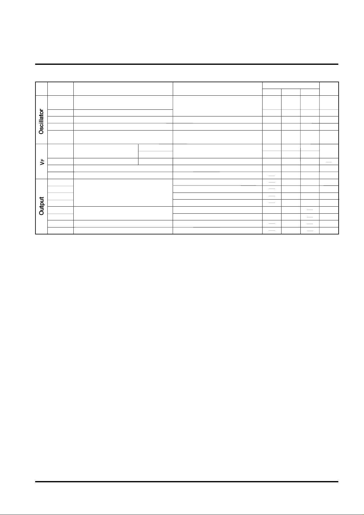
ELECTRICAL CHARACTERISTICS (VCC=18V,Ta=25˚C, unless otherwise noted)(CONTINUE)
Symbol
fOSC
TDUTY
VOSCH
VOSCL
∆VOSC
fOSCVF
TVFDUTY
VTHTIME
IVF
VOL1
VOL2
VOL3
VOL4
VOH1
VOH2
TRISE
TFALL
Oscillating frequency
Maximum ON duty
Upper limit voltage of oscillation waveform
Lower limit voltage of oscillation waveform
Voltage difference between upper limit and
lower limit of OSC waveform
OSC frequency in CLM
operating state
Duty in CLM operating state
VF voltage at timer operating start
VF terminal input current
Output low voltage
Output high voltage
Output voltage rise time
Output voltage fall time
VF=5V
VF=2V
VF=0.2V
RON=20kΩ,ROFF=17kΩ
CF=220pF,-5≤Ta≤85°C
fOSC=188kHz
fOSC=188kHz
fOSC=188kHz
RON=20kΩ,ROFF=17kΩ
CF=220pF
Min off duty/Max on duty
Source current
Vcc=18V,Io=10mA
Vcc=18V,Io=100mA
Vcc=5V,Io=1mA
Vcc=5V,Io=100mA
Vcc=18V,Io=-10mA
Vcc=18V,Io=-100mA
No load
No load
Test conditions
M51995AP/FP
Limits
Min. Typ. Max.
170 188 207
47.0 50.0 53.0
3.97 4.37 4.77
1.76 1.96 2.16
2.11
170
108
11.0 13.7
2.7
16.0
15.5
2.41 2.71
188 207
124 143
22.0
3.0
0.05
0.7
0.69
1.3
16.5
16.0
50
35
3.3
2
0.4
1.4
1.0
2.0
UnitParameter
kHz
kHz
6
%
V
V
V
V
µA
V
V
V
V
V
V
ns
ns
( / 27 )
4
SWITCHING REGULATOR CONTROL
TYPICAL CHARACTERISTICS
0
threshold voltage
(VTHOVPL)
ROFF=20kΩ
Ta=-30°C
Ta=25°C
Ta=85°C
fOSC=500kHz
fOSC=100kHz
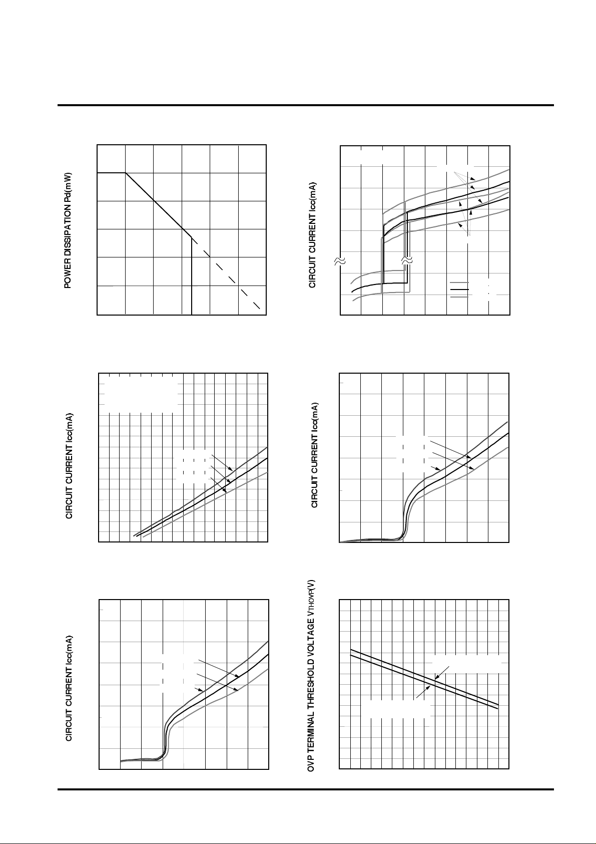
THERMAL DERATING
1800
1500
1200
(MAXIMUM RATING)
MITSUBISHI (Dig./Ana. INTERFACE)
M51995AP/FP
CIRCUIT CURRENT VS.SUPPLY VOLTAGE
22m
18m
16m
14m
(NORMAL OPERATION)
RON=18kΩ
900
600
300
0
0 25 50 75
AMBIENT TEMPERATURE Ta(°C)
CIRCUIT CURRENT VS.SUPPLY VOLTAGE
8.0
OVP RESET POINT
8.87V(-30°C)
7.0
8.94V(25°C)
9.23V(85°C)
6.0
5.0
4.0
3.0
2.0
(OVP OPERATION)
85
Ta=-30°C
Ta=25°C
Ta=85°C
100
125 150
12m
10m
100µ
50µ
0
CIRCUIT CURRENT VS.SUPPLY VOLTAGE
3.0
2.0
1.0
10
SUPPLY VOLTAGE Vcc(V)
20 30
(OFF STATE)
Ta=25°C
Ta=85°C
Ta=-30°C
40
1.0
0
0
CIRCUIT CURRENT VS.SUPPLY VOLTAGE
3.0
2.0
1.0
0
0
10.0 20.0 30.0
SUPPLY VOLTAGE Vcc(V)
(TIMER OFF STATE)
Ta=25°C
Ta=85°C
Ta=-30°C
10 20 30
SUPPLY VOLTAGE Vcc(V)
40.0
40
( / 27 )
5
1.1
1.0
0.9
0.8
0.7
0.6
0.5
0.4
0.3
0
0
10 20 30
SUPPLY VOLTAGE Vcc(V)
OVP TERMINAL THRESHOLD VOLTAGE
VS.AMBIENT TEMPERATURE
H threshold voltage
L
-40 -20
AMBIENT TEMPERATURE Ta(°C)
20 40 60
40
(VTHOVPH)
80 100
SWITCHING REGULATOR CONTROL
MITSUBISHI (Dig./Ana. INTERFACE)
M51995AP/FP
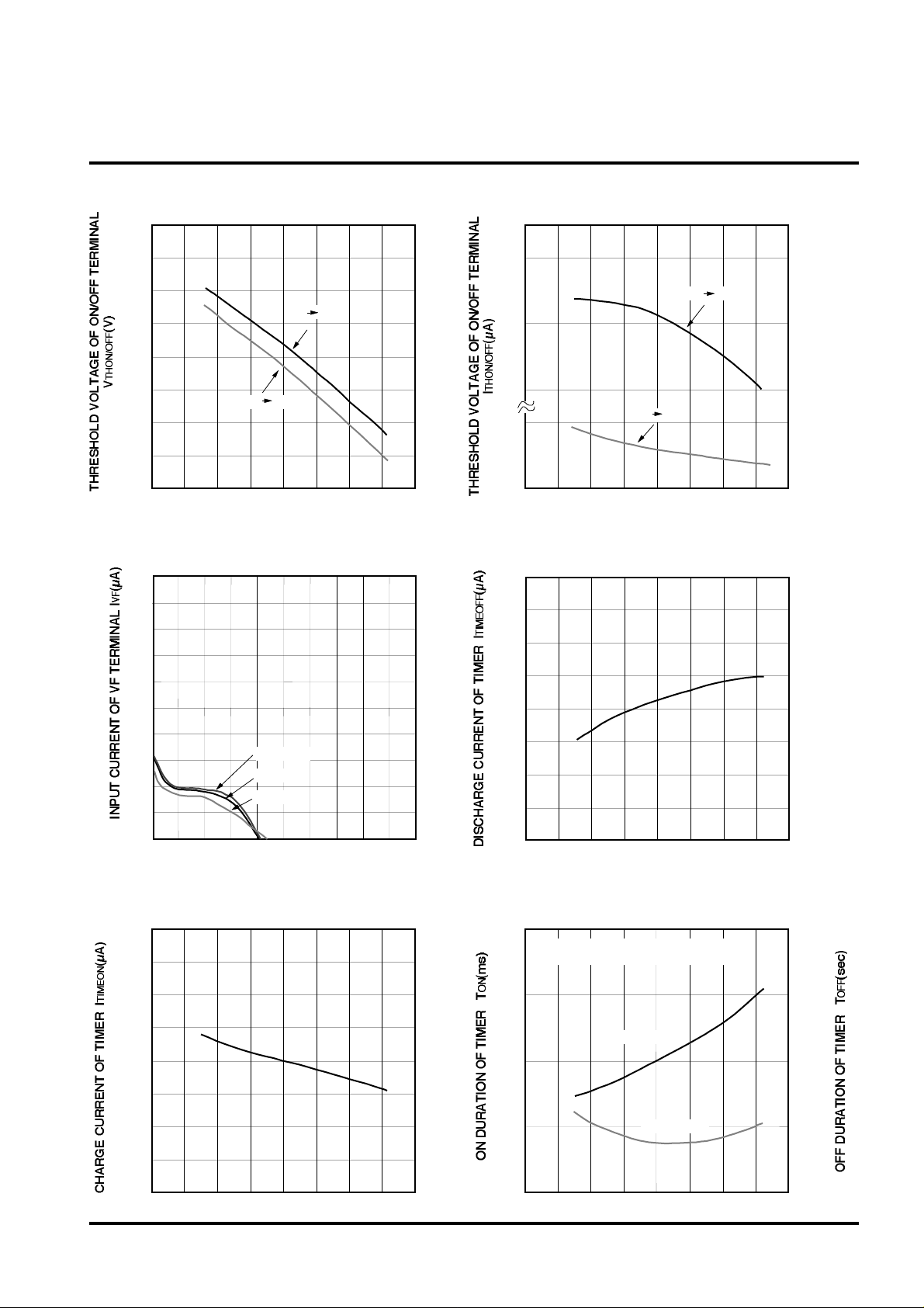
THRESHOLD VOLTAGE OF ON/OFF
TERMINAL VS.AMBIENT TEMPERATURE
3.4
3.2
3.0
ON OFF
2.8
2.6
2.4
OFF ON
2.2
2.0
1.8
-40 -20 0 20 40 60
AMBIENT TEMPERATURE Ta(°C)
INPUT CURRENT OF VF TERMINAL
-10
-9
-8
-7
-6
-5
-4
-3
-2
-1
VS.INPUT VOLTAGE
Ta=-30°C
Ta=25°C
Ta=85°C
80 100
THRESHOLD VOLTAGE OF ON/OFF
TERMINAL VS.AMBIENT TEMPERATURE
25.0
ON OFF
20.0
15.0
-20
OFF ON
20
0
40 60 80 100
5.0
0
-60
-40
AMBIENT TEMPERATURE Ta(°C)
DISCHARGE CURRENT OF TIMER
18
17
16
15
14
13
12
11
VS.AMBIENT TEMPERATURE
0
0 1 2 3 4 5 6 7 8 9 10
VF TERMINAL VOLTAGE VVF(V)
CHARGE CURRENT OF TIMER
-200
-180
-160
-140
-120
-100
-80
-60
-40
-60
VS.AMBIENT TEMPERATURE
-40 -20
0 20 40
60
AMBIENT TEMPERATURE Ta(°C)
80 100
( / 27 )
6
10
-60 -40
-20 0 20 40 60
AMBIENT TEMPERATURE Ta(°C)
ON AND OFF DURATION OF TIMER
VS.AMBIENT TEMPERATURE
175
150
(INTERMITTENT OPERATION)
TIMER ON•••CIRCUIT OPERATION ON
TIMER OFF••CIRCUIT OPERATION OFF
TIMER ON
125
100
75
-40 -20
-60
TIMER OFF
0 20 40
AMBIENT TEMPERATURE Ta(°C)
60
80
100
80 100
1.4
1.3
1.2
1.1
1.0
SWITCHING REGULATOR CONTROL
MITSUBISHI (Dig./Ana. INTERFACE)
M51995AP/FP
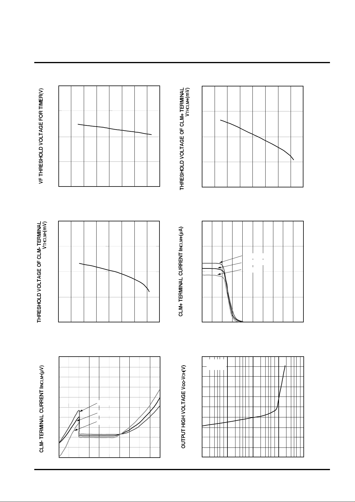
VF THRESHOLD VOLTAGE FOR TIMER
VS. AMBIENT TEMPERATURE
3.5
3.0
2.5
-40 -20 0 20 40 60 80
-60
AMBIENT TEMPERATURE Ta(°C)
THRESHOLD VOLTAGE OF CLM- TERMINAL
VS. AMBIENT TEMPERATURE
205
200
100
THRESHOLD VOLTAGE OF CLM+ TERMINAL
VS. AMBIENT TEMPERATURE
205
200
195
-40 -20 0 20 40 60 80
-60
AMBIENT TEMPERATURE Ta(°C)
CLM+ TERMINAL CURRENT
-400
-300
-200
VS. CLM+ TERMINAL VOLTAGE
Ta=-30°C
Ta=25°C
Ta=85°C
100
195
-40 -20 0 20 40 60 80
-60
AMBIENT TEMPERATURE Ta(°C)
CLM- TERMINAL CURRENT
-500
-400
-300
-200
-100
0
VS. CLM- TERMINAL VOLTAGE
Ta=-30°C
Ta=25°C
Ta=85°C
0 -0.2 -0.4 -0.6 -0.8
CLM- TERMINAL VOLTAGE VCLM-(V) OUTPUT SOURCE CURRENT IOH(A)
100
-1.0
( / 27 )7
-100
0
0
0.1 0.2
2.6
Vcc=18V
2.4
Ta=25°C
2.2
2.0
1.8
1.6
1.4
1.2
1.0
0.8
0.6
1m 10m
0.3
0.4 0.5 0.6 0.7 0.8 0.9
CLM+ TERMINAL VOLTAGE VCLM+(V)
OUTPUT HIGH VOLTAGE VS.
OUTPUT SOURCE CURRENT
100m
1 10
1.0

SWITCHING REGULATOR CONTROL
MITSUBISHI (Dig./Ana. INTERFACE)
M51995AP/FP
OUTPUT LOW VOLTAGE
5.0
4.0
3.0
2.0
1.0
0
1m
1.6
1.5
1.4
VS. OUTPUT SINK CURRENT
Ta=25°C
Vcc=18V
Vcc=5V
10m 100m 1
OUTPUT SINK CURRENT IOL(A)
INPUT CURRENT OF DETECTION AMP
VS. AMBIENT TEMPERATURE
10
2.55
2.50
2.45
2.40
50.0
40.0
DETECTION VOLTAGE
VS. AMBIENT TEMPERATURE
-40 -20 0 20 40 60 80
-60
AMBIENT TEMPERATURE Ta(°C)
DETECTION AMP VOLTAGE GAIN
VS. FREQUENCY
100
1.3
1.2
1.1
1.0
0.9
0.8
-40 -20 0 20 40 60 80
-60
AMBIENT TEMPERATURE Ta(°C)
VS. F/B TERMINAL INPUT CURRENT
50
40
30
20
ON duty
(fOSC=100kHz)
RON=18kΩ
ROFF=20kΩ
Ta=-30°C
Ta=25°C
Ta=85°C
100
30.0
20.0
10.0
0
20
100
50
40
30
1k 10k 100k 1M 10M
FREQUENCY f(Hz)
ON duty
VS. F/B TERMINAL INPUT CURRENT
(fOSC=200kHz)
RON=18kΩ
ROFF=20kΩ
Ta=-30°C
Ta=25°C
Ta=85°C
10
0
0 0.5
F/B TERMINAL INPUT CURRENT IF/B (mA)
1.0
1.5 2.0
2.5
10
( / 27 )
8
0
0 0.5
F/B TERMINAL INPUT CURRENT IF/B (mA)
1.0
1.5 2.0
2.5
SWITCHING REGULATOR CONTROL
MITSUBISHI (Dig./Ana. INTERFACE)
333333557
7
M51995AP/FP
50
40
30
20
10
0
10000
1000
100
10
1
120
110
F/B TERMINAL INPUT CURRENT
0 0.5 1.0 1.5 2.0 2.5
F/B TERMINAL INPUT CURRENT IF/B(mA)
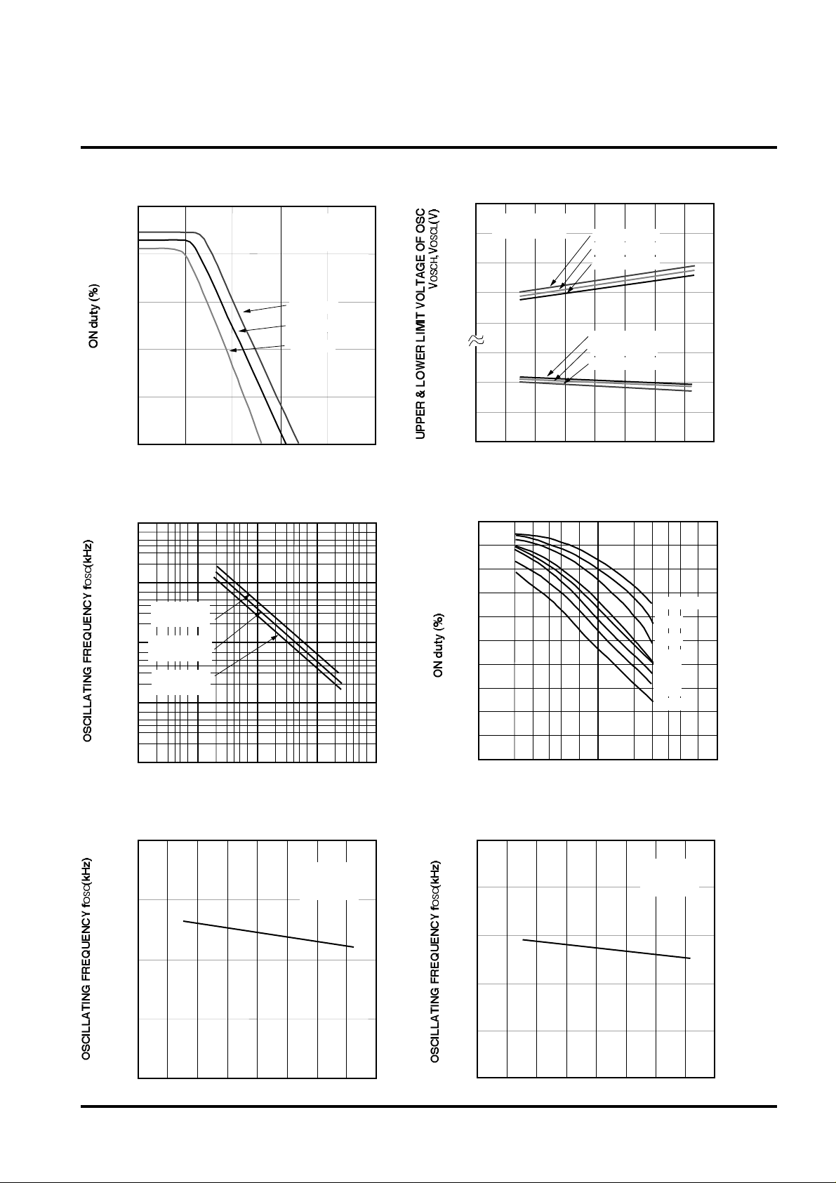
OSCILLATING FREQUENCY VS. CF
RON=22kΩ
ROFF=12kΩ
RON=36kΩ
ROFF=6.2kΩ
RON=24kΩ
ROFF=20kΩ
1 10 100 1000 10000
CF TERMINAL CAPACITY(pF)
OSCILLATING FREQUENCY VS.
ON duty VS.
(fOSC=500kHz)
RON=18kΩ
ROFF=20kΩ
Ta=-30°C
Ta=25°C
Ta=85°C
TERMINAL CAPACITY
AMBIENT TEMPERATURE
RON=24kΩ
ROFF=20kΩ
CF=330pF
UPPER & LOWER LIMIT VOLTAGE OF OSC
VS. AMBIENT TEMPERATURE
RON=18kΩ
5.2
ROFF=20kΩ
4.8
4.4
4.0
2.2
2.0
1.8
-40 -20 0 20 40 60 80
-60
AMBIENT TEMPERATURE Ta(°C)
100
90
80
70
60
50
40
30
20
10
0
1 10 100
OSCILLATING FREQUENCY VS.
700
600
AMBIENT TEMPERATURE
fOSC=500kHz
fOSC=200kHz
fOSC=100kHz
fOSC=100kHz
fOSC=200kHz
fOSC=500kHz
ON duty VS. ROFF
ROFF(kΩ)
RON=75kΩ
51kΩ
36kΩ
24kΩ
22kΩ
18kΩ
15kΩ
10kΩ
RON=24kΩ
ROFF=20kΩ
CF=47pF
100
500
100
400
90
80
-40 -20 0 20 40 60 80
-60
AMBIENT TEMPERATURE Ta(°C)
100
( / 27 )
9
300
200
-40 -20 0 20 40 60 80
-60
AMBIENT TEMPERATURE Ta(°C)
100
 Loading...