Mitsubishi M51660L Datasheet

MITSUBISHI <CONTROL / DRIVER IC>
)
(
)
t
(1)
(2)
M51660L
SERVO MOTOR CONTROL FOR RADIO CONTROL
DESCRIPTION
The M51660L is a semiconductor integrated circuit for use in servo
motor control in radio control applications.
Housed in a 14-pin molded plastic zig-zag inline package (ZIP), the
M51660L contributes to the miniaturization of the set.
The built-in voltage regulating circuit, and the differential
comparator used in the comparator circuit provide the M51660L
with extremely stable power supply voltage fluctuation
characteristics and temperature change characteristics.
FEATURES
●Small circuit current • • • • • • • • • • • • • • • • • • • • • • • • • • • • • • • • • • • • • 3.5mA typ.
(When output is off)
●Excellent power supply and temperature stability
●Simple setting of dead band
●Includes protection circuit for continuous “H” level input
APPLICATION
Digital proportional system for radio control, and servo motor
control circuit, etc.
RECOMMENDED OPERATING CONDITIONS
Supply voltage range •••••••••••••••••••••••••••••••••••••••3.5–7V
Rated supply voltage •••••••••••••••••••••••••••••••••••••••••• 4.8V
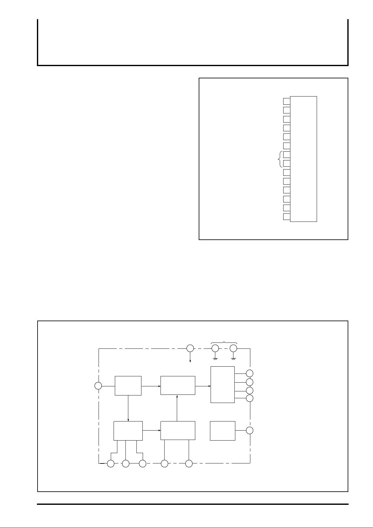
PIN CONFIGURATION(TOP VIEW
Servo position voltage
Timing capacitor
Timing resistor
External PNP transistor drive (1)
Output (1)
Error pulse output
Output (2)
Stretcher input
External PNP transistor drive (2)
Regulated voltage output
Input
GND
Supply
1
2
3
4
5
6
7
8
9
10
11
12
13
14
Outline 14P5A
M51660L
BLOCK DIAGRAM
Inpu
5
Servo position
voltage input
Control
logic
circuit
One-shot
multivibrator
Timing
capacitance
Timing
resistor
Flip-flop
Pulse
stretcher
91 2 3
Error pulse
output
Supply
4.8V
VCC
11
Stretcher
input
GND
Output
drive
circuit
Voltage
regulating
circuit
8714
External PNP transistor drive
4
Output (1)
6
10
Output (2)
External PNP transistor drive
12
Regulated voltage output
13

MITSUBISHI <CONTROL / DRIVER IC>
)
)
)
SERVO MOTOR CONTROL FOR RADIO CONTROL
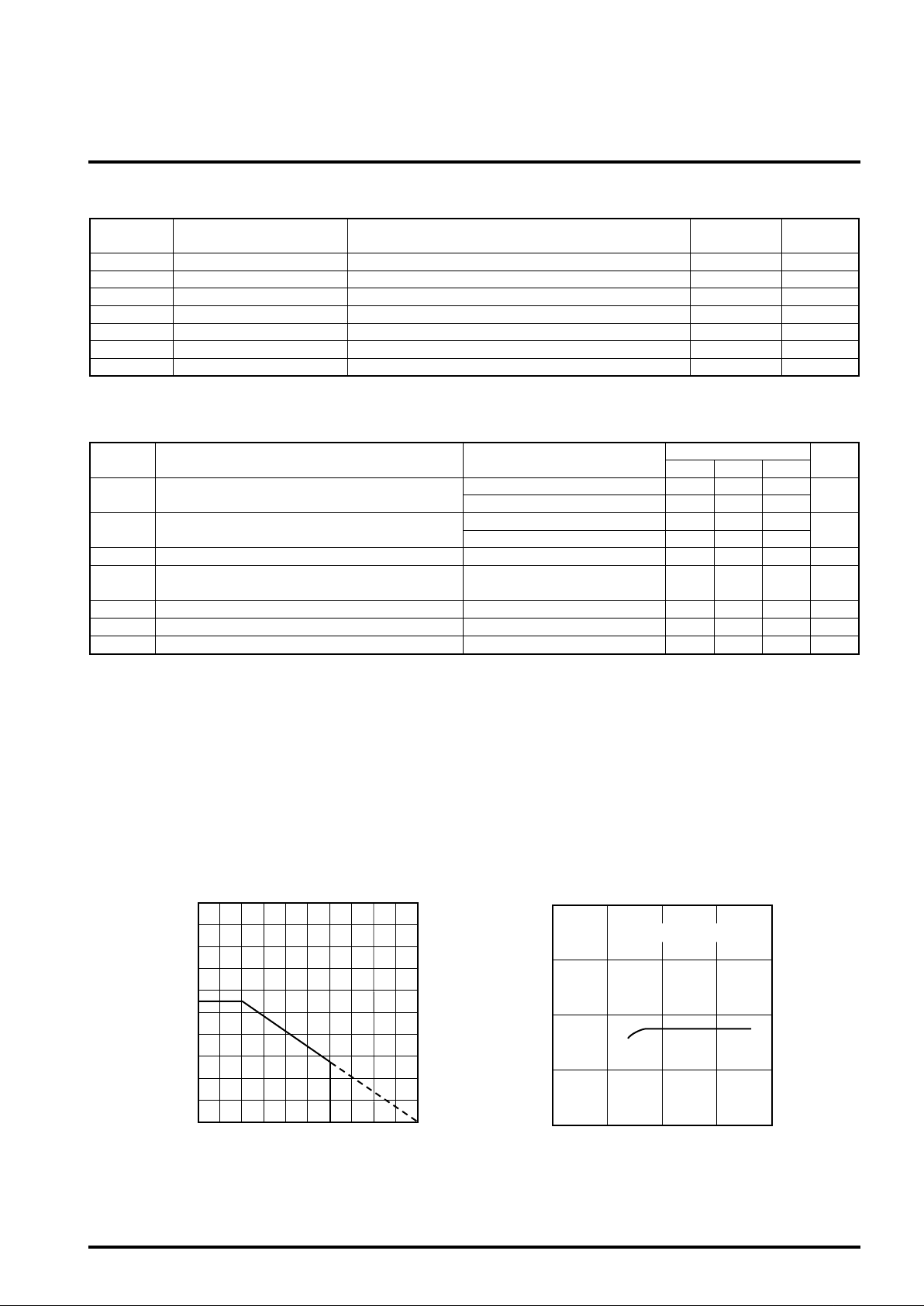
ABSOLUTE MAXIMUM RATINGS(Ta = 25°C, unless otherwise noted
M51660L
Symbol
IO SINK
IO SOURSE
Pd
Kθ
Topr
Tstg
Supply voltageVCC
Output sink current
Output source current
Power dissipation
Thermal derating range
Operating temperature
Storage temperature range
Parameter Conditions
Ta ≥ 25°C
Ratings
7.5 V
500
200
550
5.5
-20 – +75
-40 – +125
ELECTRICAL CHARACTERISTICS(Ta = 25°C and VCC = 4.8V, unless otherwise noted
Symbol Test conditions UnitParameter
CC Circuit current
I
OL Output voltage “L”
OH IO SOURCE = 100mA 3.8
Output voltage “H”
When output is OFF 3.5 5
When output is ON
I
O SINK = 100mA 0.1 0.2
I
O SINK = 400mA 0.4 0.7
External PNP transistor
Drive current
Reg Internal regulated supply voltage 2.45 2.6
Reg Internal regulated supply output current 3.0
DB Minimum dead band width
RDB = 510Ω, CS = 0.1µF 1.5
Limits
Min. Typ. Max.
20
3.4
30
2.3
Unit
mA
mA
mW
mW/°C
°C
°C
mA
VV
VV
mAIPNP
VV
mAI
µsT
TYPICAL CHARACTERIS TICS(Ta = 25°C, unless otherwise noted
Thermal derating (maximum rating)
1000
800
600
400
200
Internal power dissipation Pd (mW)
0
0 25 50 75 100 125
Ambient temperature Ta (°C)
Circuit current ICC (mA)
8
6
4
2
0
Circuit current vs. supply voltage
When output is OFF
02468
Supply voltage VCC (V)
 Loading...