

Mitsubishi M38C37MCMXXXFS, M38C37MCMXXXFP, M38C37MCAXXXFS, M38C37MBMXXXFS, M38C37MBMXXXFP Datasheet
...
MITSUBISHI MICROCOMPUTERS
38C3 Group
SINGLE-CHIP 8-BIT CMOS MICROCOMPUTER
DESCRIPTION
The 38C3 group is the 8-bit microcomputer based on the 740 family
core technology.
The 38C3 group has a LCD drive control circuit, a 10-channel A-D
converter, and a Serial I/O as additional functions.
The various microcomputers in the 38C3 group include variations of
internal memory size and packaging. For details, refer to the section
on part numbering.
For details on availability of microcomputers in the 38C3 group, refer
to the section on group expansion.
FEATURES
●Basic machine-language instructions ....................................... 71
●The minimum instruction execution time............................. 0.5 µs
(at 8MHz oscillation frequency)
●Memory size
ROM ..................................................................4 K to 48 K bytes
RAM ................................................................. 192 to 1024 bytes
●Programmable input/output ports ............................................. 57
●Software pull-up/pull-down resistors
..................................................... (Ports P0–P8 except Port P5
●Interrupts................................................... 16 sources, 16 vectors
(includes key input interrupt)
●Timers ............................................................8-bit ✕ 6, 16-bit ✕ 1
●A-D converter.................................................10-bit ✕ 8 channels
●Serial I/O ....................................... 8-bit ✕ 1 (Clock-synchronized)
●LCD drive control circuit
Bias ............................................................................ 1/1, 1/2, 1/3
Duty .................................................................... 1/1, 1/2, 1/3, 1/4
Common output .......................................................................... 4
Segment output ........................................................................ 32
●2 Clock generating circuit
(connect to external ceramic resonator or quartz-crystal oscillator)
●Power source voltage
In high-speed mode ....................................................4.0 to 5.5 V
In middle-speed mode ................................................2.5 to 5.5 V
In low-speed mode...................................................... 2.5 to 5.5 V
●Power dissipation
In high-speed mode ...........................................................32 mW
(at 8 MHz oscillation frequency)
In low-speed mode..............................................................45 µW
(at 32 kHz oscillation frequency , at 3 V power source voltage)
●Operating temperature range.................................... – 20 to 85°C
APPLICATIONS
Camera, household appliances, consumer electronics, etc.
1)
PIN CONFIGURATION (TOP VIEW)
P20/SEG0
P21/SEG1
64
63
P47/SRDY
P46/SCLK1
P45/SOUT
P44/SIN
P43/φ
P42/T3OUT
P41/T1OUT
P40/SCLK2
AV
VREF
P67/AN7
P66/AN6
P65/AN5
P64/AN4
P63/AN3
P62/AN2
SS
65
66
67
68
69
70
71
72
73
74
75
76
77
78
79
80
2
1
P60/AN0
P61/AN1
P22/SEG2
P23/SEG3
62
61
P27/SEG7
P25/SEG5
58
60
57
59
P03/SEG11
P00/SEG8
P02/SEG10
54
53
56
55
P07/SEG15
P10/SEG16
P06/SEG14
50
49
52
51
48
47
P05/SEG13
P04/SEG12
P01/SEG9
P26/SEG6
P24/SEG4
M38C34M6AXXXFP
4
3
P56/INT1
P57/INT2
8
5
P55/INT0
9
6
7
P52/PWM1
P54/CNTR1
P53/CNTR0
P51
10
11
RESET
P71/XcOUT
12
P70/XcIN
16
15
XOUT
18
17
VCC
13
14
XIN
VSS
P50/TAOUT
Package type : 80P6N-A
80-pin plastic-molded QFP
P11/SEG17
P12/SEG18
46
19
P87
P86
P16/SEG22
P13/SEG19
P15/SEG21
P17/SEG23
P14/SEG20
45
44
43
42
41
40
39
38
37
36
35
34
33
32
31
30
29
28
27
26
25
22
24
21
23
20
P85
P82
P84
P83
P81
P30/SEG24
P31/SEG25
P32/SEG26
P33/SEG27
P34/SEG28
P35/SEG29
P36/SEG30
P37/SEG31
COM0
COM1
COM2
COM3
VL1
VL2
VL3
P80
Fig. 1 M38C34M6AXXXFP pin configuration
Key-on wake-up
INT0–INT
2
CNTR
0
,CNTR
1
T1
OUT,
T3
OUT
φ
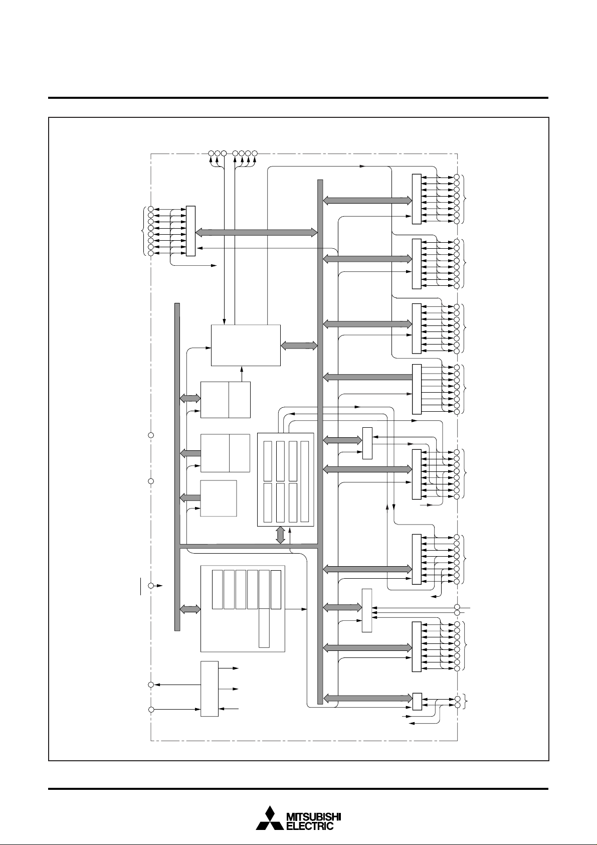
Data bus
C P U
AXY
S
PC
H
PCLPS
RESET
V
CC
V
SS
Reset input ( 5 V ) ( 0 V )
R O M
R A M
LCD display
RAM
(16 bytes)
10 16
13
I/O port P5
P4(8)
I/O port P4
I/O port P2
P2(8)
I/O port P1
P1(8)
P6(8)
Output port P3
I/O port P6
P5(8)
I/O port P7
P7(2)
2827263231
30
29
I/O port P0
P0(8)
49
50 51
52 53 54
55
5641 42 43 44 45
46 47
48
57
58
59
60
61
62 63
6467 68 69 70 71 7265
66
12
11
1
2
75 76
77
78
79
80 7374
456789
17
3
Clock generating
circuit
Main
clock
input
X
IN
Main
clock
output
X
OUT
X
COUT
Sub-
clock
output
X
CIN
Sub-
clock
input
SI/O(8)
V
REF
AV
SS
( 0 V )
A-D converter(10)
Timer 1(8) Timer 2(8)
LCD
drive control
circuit
VL1VL2V
L3
COM0COM1COM
2
COM
3
φ
X
CIN
X
COUT
14
15
Timer 3(8) Timer 4(8)
Timer 5(8) Timer 6(8)
P3(8)
33 34
35
36
37
38 39
40
R O M
corrective
circuit
ROM corrective
RAM
(8 bytes)
I/O port P8
P8(8)
18 19 20 21 22 23 24 25
PWM
0,
PWM
1
Timer A(16)
MITSUBISHI MICROCOMPUTERS
38C3 Group
SINGLE-CHIP 8-BIT CMOS MICROCOMPUTER
FUNCTIONAL BLOCK DIAGRAM
Fig. 2 Functional block diagram
2
PIN DESCRIPTION
Table 1 Pin description (1)
MITSUBISHI MICROCOMPUTERS
38C3 Group
SINGLE-CHIP 8-BIT CMOS MICROCOMPUTER
Pin
CC, VSS
V
VREF
AVSS
RESET
XIN
XOUT
VL1 – VL3
COM0 –
COM3
P00/SEG9 –
P07/SEG15
P10/SEG16 –
P17/SEG23
P20/SEG0 –
P27/SEG7
P30/SEG24 –
P37/SEG31
P40/SCLK2
P41/T1OUT
P42/T3OUT
P43/φ
P44/SIN,
P45/SOUT,
P46/SCLK1,
P47/SRDY
Name
Power source
Analog reference
voltage
Analog power
source
Reset input
Clock input
Clock output
LCD power
source
Common output
I/O port P0
I/O port P1
I/O port P2
Output port P3
I/O port P4
Function
• Apply voltage of 2.5 V to 5.5 V to VCC, and 0 V to VSS.
• Reference voltage input pin for A-D converter .
• GND input pin for A-D converter.
• Connect to VSS.
• Reset input pin for active “L.”
• Input and output pins for the main clock generating circuit.
• Feedback resistor is built in between XIN pin and XOUT pin.
• Connect a ceramic resonator or a quartz-crystal oscillator between the XIN and XOUT pins to set the
oscillation frequency.
• If an external clock is used, connect the clock source to the XIN pin and leave the XOUT pin open.
• Input 0 ≤ VL1 ≤ VL2 ≤ VL3 ≤ VCC voltage.
• Input 0 – VL3 voltage to LCD.
• LCD common output pins.
• COM1, COM2, and COM3 are not used at 1/1 duty ratio.
• COM2 and COM3 are not used at 1/2 duty ratio.
• COM3 is not used at 1/3 duty ratio.
• 8-bit I/O port.
• CMOS compatible input level.
• CMOS 3-state output structure.
• I/O direction register allows each port to be individually
programmed as either input or output.
• Pull-down control is enabled.
• 8-bit output port.
• CMOS state output.
• Pull-down control is enabled.
• 8-bit I/O port.
• CMOS compatible input level.
• CMOS 3-state output structure.
• I/O direction register allows each pin to be individually
programmed as either input or output.
• Pull-up control is enabled.
Function except a port function
• LCD segment pins
• Serial I/O function pin
• Timer output pin
• Timer output pin
• φ output pin
• Serial I/O function pins
3
Table 2 Pin description (2)
MITSUBISHI MICROCOMPUTERS
38C3 Group
SINGLE-CHIP 8-BIT CMOS MICROCOMPUTER
Pin
P51
P50/TAOUT
P52/PWM1
P53/CNTR0,
P54/CNTR1
P55/INT0,
P56/INT1,
P57/INT2
P60/AN0 –
P67/AN7
P70/XCOUT,
P71/XCIN
P80 – P87
Name
Input port P5
I/O port P5
I/O port P6
I/O port P7
I/O port P8
Function
• 1-bit input pin.
• CMOS compatible input level.
• 7-bit I/O port.
• CMOS compatible input level.
• CMOS 3-state output structure.
• I/O direction register allows each pin to be individually
programmed as either input or output.
• Pull-up control is enabled.
• 8-bit I/O port.
• CMOS compatible input level.
• CMOS 3-state output structure.
• I/O direction register allows each pin to be individually
programmed as either input or output.
• Pull-up control is enabled.
• 2-bit I/O port.
• CMOS compatible input level.
• CMOS 3-state output structure.
• I/O direction register allows each pin to be individually
programmed as either input or output.
• Pull-up control is enabled.
• 8-bit I/O port.
• TTL input level.
• CMOS 3-state output structure.
• I/O direction register allows each pin to be individually
programmed as either input or output.
• Pull-up control is enabled.
Function except a port function
• Timer A output pin
• PWM1 output (timer output) pin
• External count I/O pins
• External interrupt input pins
• A-D conversion input pins
• Sub-clock generating circuit I/O pins
• Key input (Key-on wake-up) interrupt
input pins
4
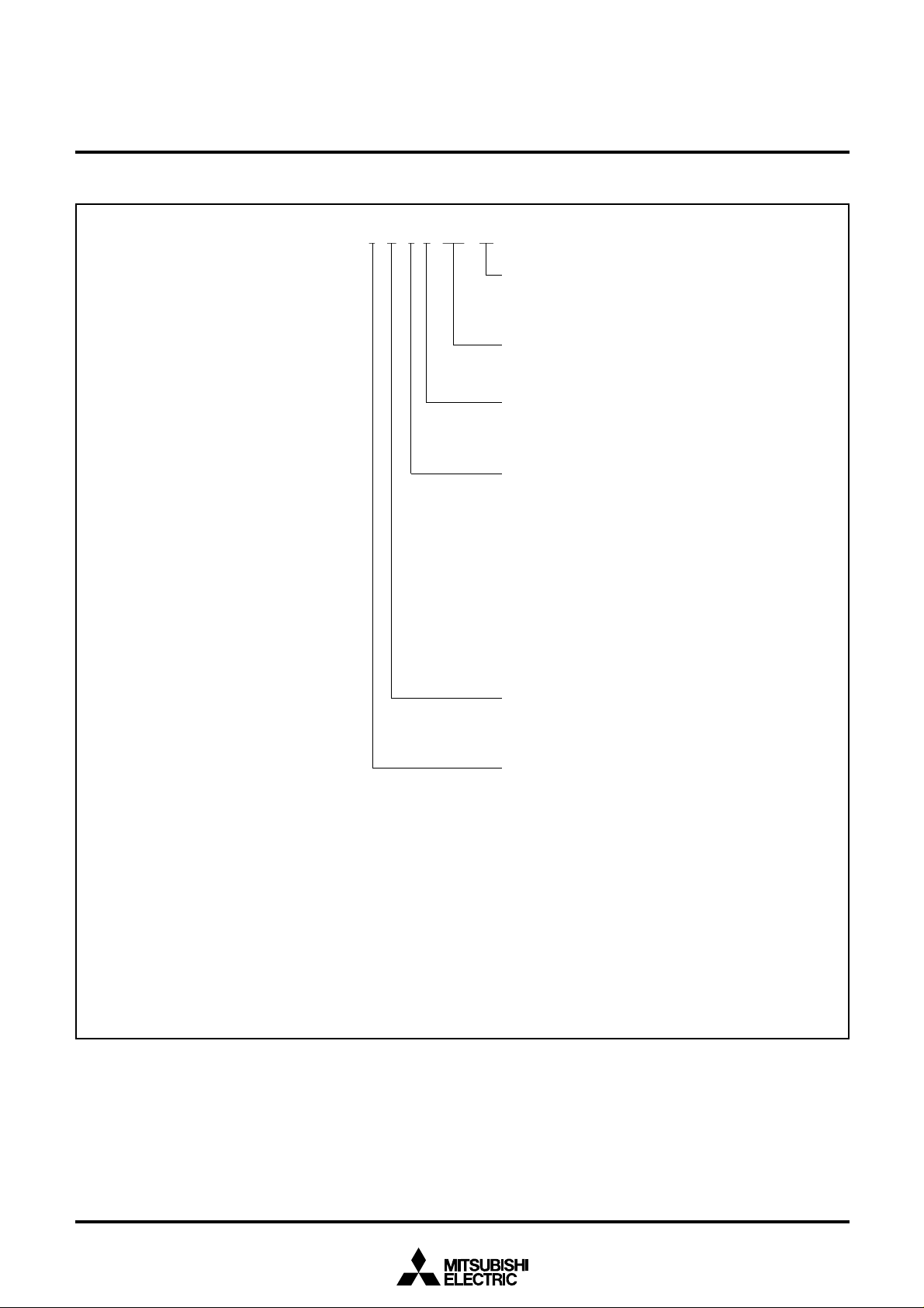
P ART NUMBERING
MITSUBISHI MICROCOMPUTERS
38C3 Group
SINGLE-CHIP 8-BIT CMOS MICROCOMPUTER
M38C3 4 M 6 A XXX FPProduct
Package type
: 80P6N-A package
FP
: 80D0 package
FS
ROM number
Omitted in some types.
A : Standard(Note)
M : M version
ROM/PROM size
1
: 4096 bytes
2
: 8192 bytes
3
: 12288 bytes
4
: 16384 bytes
5
: 20480 bytes
6
: 24576 bytes
7
: 28672 bytes
8
: 32768 bytes
The first 128 bytes and the last 2 bytes of ROM
are reserved areas ; they cannot be used.
Memory type
ME : Mask ROM version
: EPROM or One Time PROM version
RAM size
0
: 192 bytes
1
: 256 bytes
2
: 384 bytes
3
: 512 bytes
4
: 640 bytes
5
: 768 bytes
6
: 896 bytes
7
: 1024 bytes
9
: 36864 bytes
A
: 40960 bytes
B
: 45056 bytes
C
: 49152 bytes
Fig. 3 Part numbering
Note : Difference between standard and M version
• Standard :
• M version :
Port P50/TA
register is set to the output mode during reset and after
reset.
Port P5
the direction register is set to the input mode during reset
and after reset.
OUT
pin remains set to the input mode until the direction
0
/TA
OUT
pin remains set to the output mode (“L” output) until
5
MITSUBISHI MICROCOMPUTERS
38C3 Group
SINGLE-CHIP 8-BIT CMOS MICROCOMPUTER
GROUP EXPANSION
Mitsubishi plans to expand the 38C3 group as follows.
Memory T ype
Support for mask ROM, One Time PROM, and EPROM versions
Memory Size
ROM/PROM size ................................................ 16 K to 48 K bytes
RAM size............................................................. 512 to 1024 bytes
Memory Expansion Plan
ROM size (bytes)
48K
44K
40K
36K
32K
28K
24K
20K
16K
12K
8K
4K
Planning
Packages
80P6N-A ..................................... 0.8 mm-pitch plastic molded QFP
80D0 ........................ 0.8 mm-pitch ceramic LCC (EPROM version)
Under development
M38C37ECA/ECM
Under development
M38C34M6A/M6M
M38C33M4
192
Products under development or planning : the development schedule and specification may be revised without notice.
Planning products may be stopped the development.
Fig. 4 Memory expansion plan
Currently planning products are listed below.
Table 3 Support products
Product name
M38C34M6AXXXFP
M38C37ECAXXXFP
M38C37ECAFP
M38C37ECAFS
M38C34M6MXXXFP
M38C37ECMXXXFP
M38C37ECMFP
M38C37ECMFS
(P) ROM size (bytes)
ROM size for User in ( )
24576 (24446)
49152 (49022)
24576 (24446)
49152 (49022)
256 384 512 640 768 896
RAM size (bytes)
RAM size
(bytes)
640
1024
640
1024
Package
80P6N-A
80D0
80P6N-A
80D0
Mask ROM version
One Time PROM version
One Time PROM version (blank)
EPROM version
Mask ROM version
One Time PROM version
One Time PROM version (blank)
EPROM version
1024
As of April 1998
Remarks
6
FUNCTIONAL DESCRIPTION
CENTRAL PROCESSING UNIT (CPU)
The 38C3 group uses the standard 740 family instruction set. Refer
to the table of 740 family addressing modes and machine instructions or the 740 Family Software Manual for details on the instruction
set.
Machine-resident 740 family instructions are as follows:
The FST and SLW instruction cannot be used.
The STP, WIT, MUL, and DIV instruction can be used.
[CPU Mode Register (CPUM)] 003B16
The CPU mode register contains the stack page selection bit and the
internal system clock selection bit.
The CPU mode register is allocated at address 003B
16.
MITSUBISHI MICROCOMPUTERS
38C3 Group
SINGLE-CHIP 8-BIT CMOS MICROCOMPUTER
b7 b0
Fig. 5 Structure of CPU mode register
CPU mode register
(CPUM (CM) : address 003B
Processor mode bits
b1 b0
0 0 : Single-chip mode
0 1 :
1 0 :
1 1 :
Stack page selection bit
0 : RAM in the zero page is used as stack area
1 : RAM in page 1 is used as stack area
Not used (returns “1” when read)
(Do not write “0” to this bit.)
Port X
0 : I/O port
1 : X
Main clock ( X
0 : Operating
1 : Stopped
Main clock division ratio selection bit
0 : f(X
1 : f(X
Internal system clock selection bit
0 : X
1 : X
Not available
C
switch bit
CIN
, X
COUT
IN–XOUT
IN
)/2 (high-speed mode)
IN
)/8 (middle-speed mode)
IN-XOUT
selected (middle-/high-speed mode)
CIN-XCOUT
16
)
) stop bit
selected (low-speed mode)
7
MITSUBISHI MICROCOMPUTERS
38C3 Group
SINGLE-CHIP 8-BIT CMOS MICROCOMPUTER
MEMORY
Special Function Register (SFR) Area
The Special Function Register area in the zero page contains control
registers such as I/O ports and timers.
RAM
RAM is used for data storage and for stack area of subroutine calls
and interrupts.
ROM
The first 128 bytes and the last 2 bytes of ROM are reserved for
device testing and the rest is user area for storing programs.
Interrupt Vector Area
The interrupt vector area contains reset and interrupt vectors.
RAM area
RAM size
(bytes)
192
256
384
512
640
768
896
1024
Address
XXXX
00FF
013F
01BF
023F
02BF
033F
03BF
043F
16
16
16
16
16
16
16
16
16
Zero Page
Access to this area with only 2 bytes is possible in the zero page
addressing mode.
Special Page
Access to this area with only 2 bytes is possible in the special page
addressing mode.
0000
16
SFR area 1
0040
16
RAM
0050
0058
0100
XXXX
LCD display RAM area
16
ROM corrective RAM area
16
16
16
(Note 1)
Reserved area
Zero page
ROM area
ROM size
(bytes)
Address
YYYY
4096
8192
12288
16384
20480
24576
28672
32768
36864
40960
45056
49152
Note 1 : This is valid only in mask ROM version.
Fig. 6 Memory map diagram
F000
E000
D000
C000
B000
A000
9000
8000
7000
6000
5000
4000
0440
16
16
0F00
0FFF
16
16
16
16
16
16
16
16
16
16
16
16
16
Address
ZZZZ
F080
E080
D080
C080
B080
A080
9080
8080
7080
6080
5080
4080
16
16
16
16
16
16
16
16
16
16
16
16
16
ROM
YYYY
ZZZZ
FF00
FFDC
FFFE
FFFF
16
16
16
16
16
16
16
Not used
SFR area 2 (Note 1)
Reserved ROM area
(128 bytes)
Interrupt vector area
Reserved ROM area
Special page
8

MITSUBISHI MICROCOMPUTERS
38C3 Group
SINGLE-CHIP 8-BIT CMOS MICROCOMPUTER
Port P0 (P0)
0000
16
Port P0 direction register (P0D)
0001
16
Port P1 (P1)
0002
16
Port P1 direction register (P1D)
0003
16
Port P2 (P2)
0004
16
Port P2 direction register (P2D)
0005
16
Port P3 (P3)
0006
16
0007
16
Port P4 (P4)
0008
16
Port P4 direction register (P4D)
0009
16
Port P5 (P5)
000A
16
Port P5 direction register (P5D)
000B
16
Port P6 (P6)
000C
16
Port P6 direction register (P6D)
000D
16
Port P7 (P7)
000E
16
Port P7 direction register (P7D)
000F
16
0010
16
Port P8 (P8)
Port P8 direction register (P8D)
0011
16
0012
16
0013
16
0014
16
0015
16
PULL register A (PULLA)
0016
16
PULL register B (PULLB)
0017
16
Port P8 output selection register (P8SEL)
0018
16
Serial I/O control register 1 (SIOCON1)
0019
16
Serial I/O control register 2 (SIOCON2)
001A
16
Serial I/O register (SIO)
001B
16
001C
16
001D
16
001E
16
001F
16
16
0020
Timer 1 (T1)
Timer 2 (T2)
0021
16
Timer 3 (T3)
0022
16
Timer 4 (T4)
0023
16
0024
16
Timer 5 (T5)
Timer 6 (T6)
0025
16
0026
16
Timer 6 PWM register (T6PWM)
0027
16
Timer 12 mode register (T12M)
0028
16
Timer 34 mode register (T34M)
0029
16
Timer 56 mode register (T56M)
002A
16
φ output control register (CKOUT)
002B
16
Timer A register (low) (TAL)
002C
16
Timer A register (high) (TAH)
002D
16
Compare register (low) (CONAL)
002E
16
Compare register (high) (CONAH)
002F
16
Timer A mode register (TAM)
0030
16
Timer A control register (TACON)
0031
16
A-D control register (ADCON)
0032
16
0033
16
A-D conversion register (low) (ADL)
A-D conversion register (high) (ADH)
0034
16
0035
16
0036
16
0037
16
Segment output enable register (SEG)
0038
16
LCD mode register (LM)
0039
16
Interrupt edge selection register (INTEDGE)
003A
16
CPU mode register (CPUM)
003B
16
Interrupt request register 1 (IREQ1)
003C
16
Interrupt request register 2 (IREQ2)
003D
16
Interrupt control register 1 (ICON1)
003E
16
Interrupt control register 2 (ICON2)
003F
16
ROM correct enable register 1 (Note)
0F01
16
ROM correct high-order address register 1 (Note)
0F02
16
ROM correct low-order address register 1 (Note)
0F03
16
ROM correct high-order address register 2 (Note)
0F04
16
0F05
16
ROM correct low-order address register 2 (Note)
ROM correct high-order address register 3 (Note)
0F06
16
ROM correct low-order address register 3 (Note)
0F07
16
ROM correct high-order address register 4 (Note)
0F08
16
ROM correct low-order address register 4 (Note)
0F09
16
Note: This register is valid only in mask ROM version.
Fig. 7 Memory map of special function register (SFR)
0F0A
16
ROM correct high-order address register 5 (Note)
0F0B
16
ROM correct low-order address register 5 (Note)
0F0C
16
ROM correct high-order address register 6 (Note)
0F0D
16
ROM correct low-order address register 6 (Note)
0F0E
16
ROM correct high-order address register 7 (Note)
ROM correct low-order address register 7 (Note)
0F0F
16
0F10
16
ROM correct high-order address register 8 (Note)
ROM correct low-order address register 8 (Note)
0F11
16
9
I/O PORTS
[Direction Registers (ports P2, P4, P5
0, P52–P57,
and P6–P8)]
The I/O ports P2, P4, P50, P52–P57, and P6–P8 have direction registers which determine the input/output direction of each individual
pin. Each bit in a direction register corresponds to one pin, each pin
can be set to be input port or output port.
When “0” is written to the bit corresponding to a pin, that pin becomes an input pin. When “1” is written to that bit, that pin becomes
an output pin.
If data is read from a pin set to output, the value of the port output
latch is read, not the value of the pin itself. Pins set to input are floating. If a pin set to input is written to, only the port output latch is
written to and the pin remains floating.
[Direction Registers (ports P0 and P1)]
Ports P0 and P1 have direction registers which determine the input/
output direction of each individual port.
Each port in a direction register corresponds to one port, each port
can be set to be input or output.
When “0” is written to the bit 0 of a direction register, that port becomes an input port. When “1” is written to that port, that port becomes an output port. Bits 1 to 7 of ports P0 and P1 direction registers are not used.
Pull-up/Pull-down Control
By setting the PULL register A (address 001616) or the PULL register
B (address 0017
16), ports except for ports P3 and P51 can control
either pull-down or pull-up (pins that are shared with the segment
output pins for LCD are pull-down; all other pins are pull-up) with a
program.
However, the contents of PULL register A and PULL register B do
not affect ports programmed as the output ports.
Port P8 Output Selection
Ports P80 to P87 can be switched to N-channel open-drain output by
setting “1” to the port P8 output selection register.
MITSUBISHI MICROCOMPUTERS
38C3 Group
SINGLE-CHIP 8-BIT CMOS MICROCOMPUTER
b7 b0
b7 b0
Note : The contents of PULL register A and PULL register B
do not affect ports programmed as the output ports.
Fig. 8 Structure of PULL register A and PULL register B
b7 b0
Fig. 9 Structure of port P8 output selection register
PULL register A
(PULLA : address 0016
P00–P07 pull-down
P1
0
–P17 pull-down
0
–P27 pull-down
P2
Not used
P7
0
, P71 pull-up
P8
0
–P87 pull-up
Not used (return “0” when read)
PULL register B
(PULLB : address 0017
P40–P43 pull-up
P4
4
–P47 pull-up
P5
0
, P52, P53 pull-up
4
–P57 pull-up
P5
P6
0
, P63 pull-up
P6
4
–P67 pull-up
Not used (return “0” when read)
0 : Disable
1 : Enable
Port P8 output selection register
(P8SEL : address 0018
0 : CMOS output (in output mode)
1 : N-channel open-drain output
(in output mode)
16
)
16
)
16)
Table 4 List of I/O port function (1)
Pin
P00/SEG8 –
Name
Port P0
Input/Output
Input/Output,
P07/SEG15
P10/SEG16 –
Port P1
Input/Output,
P17/SEG23
P20/SEG0 –
P27/SEG7
P30/SEG24 –
P37/SEG31
Port P2
Port P3
Input/Output,
individual bits
individual bits
10
port unit
port unit
Output,
I/O format
CMOS compatible input
level
CMOS 3-state output
CMOS compatible input
level
CMOS 3-state output
CMOS compatible input
CMOS 3-state output
CMOS 3-state output
Non-port function
LCD segment output
LCD segment output
LCD segment output
LCD segment output
Related SFRs
PULL register A
Segment output enable register
PULL register A
Segment output enable register
PULL register A
Segment output enable register
Segment output enable register
Ref. No.
(1)
(2)
MITSUBISHI MICROCOMPUTERS
38C3 Group
SINGLE-CHIP 8-BIT CMOS MICROCOMPUTER
Table 5 List of I/O port function (2)
Pin
P40/SCLK2
P41/T1OUT
P42/T3OUT
P43/φ
P44/SIN
P45/SOUT
P46/SCLK1
P47/SRDY
P50/TAOUT
P51
P52/PWM1
P53/CNTR0
P54/CNTR1
P55/INT0
P56/INT1
P57/INT2
P60/AN0
–
P67/AN7
P70/XCIN
P71/XCOUT
P80 – P87
COM0 – COM
Notes 1: Make sure that the input level at each pin is either 0 V or VCC during execution of the STP instruction.
When an input level is at an intermediate potential, a current will flow from V
2: For details of the functions of ports P0 to P3 in modes other than single-chip mode, and how to use double function ports as function I/O ports, refer to the
applicable sections.
3
Name
Port P4
Port P5
Port P6
Port P7
Port P8
Common
Input/Output
Input/Output,
individual bits
Input/Output,
individual bits
Input
Input/Output,
individual bits
Input/Output,
individual bits
Input/Output,
individual bits
Input/Output,
individual bits
Output
I/O format
CMOS compatible input
level
CMOS 3-state output
CMOS compatible input
level
CMOS 3-state output
CMOS compatible input
level
CMOS compatible input
level
CMOS 3-state output
CMOS compatible input
level
CMOS 3-state output
CMOS compatible input
level
CMOS 3-state output
CMOS compatible input
level
CMOS 3-state output
LCD common output
Non-port function
Serial I/O function I/O
Timer output
Timer output
φ clock output
Serial I/O function I/O
Timer A output
PWM output
External count I/O
External interrupt input
A-D converter input
Sub-clock generating
circuit I/O
Key input (key-on
wake-up) interrupt input
CC to VSS through the input-stage gate.
Serial I/O control registers
1, 2
PULL register B
Timer 12 mode register
PULL register B
Timer 34 mode register
PULL register B
φ output control register
PULL register B
Serial I/O control registers
1, 2
PULL register B
Timer A mode register
Timer A control reigster
PULL register B
Timer 56 mode register
PULL register B
Interrupt edge selection register
PULL register B
Interrupt edge selection register
PULL register B
A-D control register
PULL register B
CPU mode register
PULL register A
Interrupt control register 2
PULL register A
LCD mode register
Related SFRs
Ref. No.
(3)
(4)
(4)
(5)
(6)
(7)
(8)
(9)
(10)
(11)
(4)
(12)
(12)
(13)
(14)
(15)
(17)
(16)
11
MITSUBISHI MICROCOMPUTERS
38C3 Group
SINGLE-CHIP 8-BIT CMOS MICROCOMPUTER
(1)Ports P0, P1, P2
VL2/V
Segment output enable bit
Direction register
Data bus
Note : Port P0, P1 direction registers are only bit 0.
(3)Port P4
P-channel output disable bit
Serial I/O mode selection bit
Port latch
0
Direction register
VL1/V
(Note)
Segment output enable bit
L3
SS
Pull-down control
Pull-up control
(2)Port P3
Segment output enable bit
Data bus Port latch
(4)Ports P41, P42, P5
Timer 1 output selection bit
Timer 3 output selection bit
Timer 6 output selection bit
Direction register
VL2/V
L3
VL1/V
SS
Pull-down control
Segment output enable bit
2
Pull-up control
Data bus
(5)Port P4
Data bus
Port latch
Serial I/O clock output
3
Direction register
Port latch
φ output control bit
Fig. 10 Port block diagram (1)
Data bus
(6)Port P4
Pull-up control
Data bus
φ
Port latch
Timer 1 output
Timer 3 output
Timer 6 output
4
Direction register
Port latch
Pull-up control
Serial I/O input
12
MITSUBISHI MICROCOMPUTERS
38C3 Group
SINGLE-CHIP 8-BIT CMOS MICROCOMPUTER
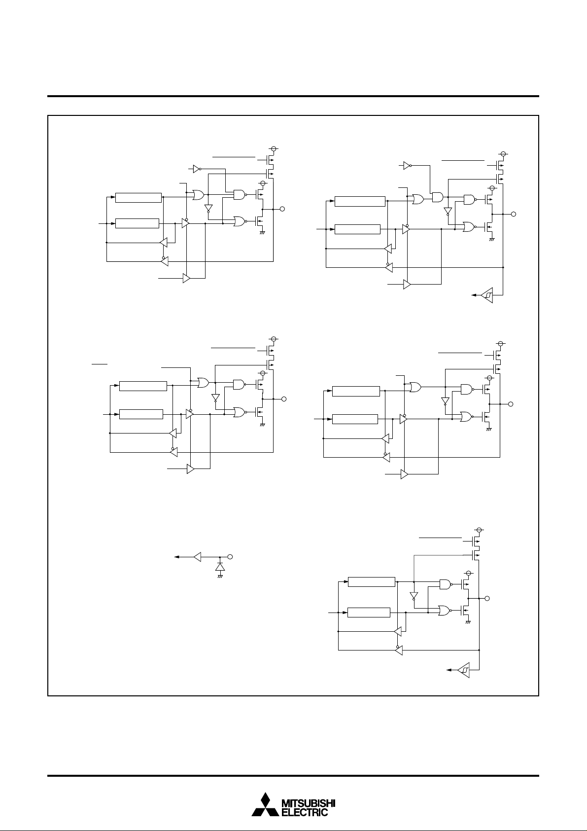
(7)Port P4
Data bus
(9)Port P4
Data bus
5
P-channel output disable bit
Serial I/O port selection bit
Serial I/O output
7
S
RDY
output enable bit
Direction register
Port latch
Direction register
Port latch
Pull-up control
Pull-up control
(8)Port P4
Data bus
(10)Port P5
Data bus
6
P-channel output disable bit
Serial I/O mode selection bit
Direction register
Serial I/O clock output
0
Timer A output enable bit
Direction register
Pull-up control
Port latch
Serial I/O clock input
Pull-up control
(Note)
Port latch
Serial I/O ready output
(11)Port P5
1
Data bus
Note: The initihal value of M version becomes “1” (output).
Fig. 11 Port block diagram (2)
Timer A output
(12)Ports P53–P5
Data bus
7
Direction register
Port latch
INT0–INT2 interrupt input
0
,CNTR1 interrupt input
CNTR
Pull-up control
13
MITSUBISHI MICROCOMPUTERS
38C3 Group
SINGLE-CHIP 8-BIT CMOS MICROCOMPUTER
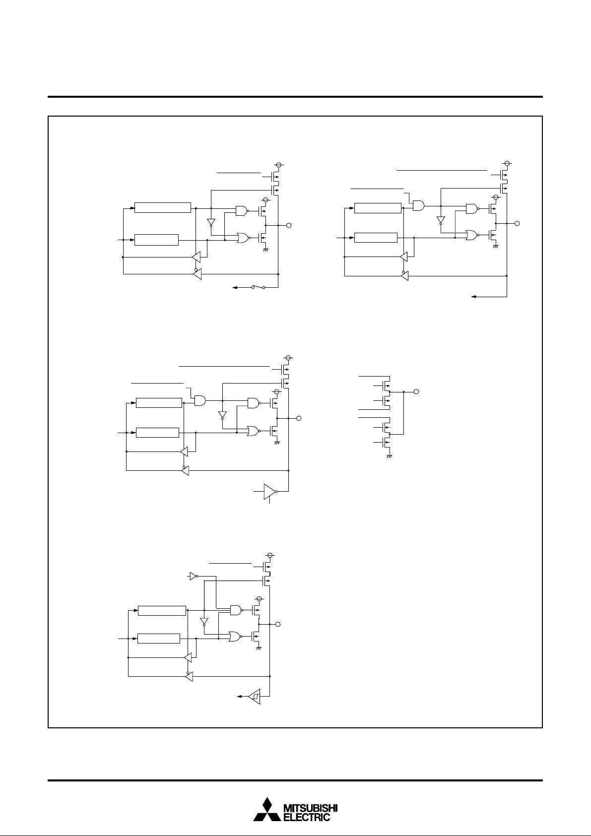
(13)Port P6
Data bus
(15)Port P7
Data bus
Direction register
Port latch
1
Port Xc switch bit
Direction register
Port latch
Pull-up control
A-D conversion input
Analog input pin selection bit
Port selection • pull-up control
(14)Port P7
Data bus
(16)COM0–COM
0
Port selection • pull-up control
Port Xc switch bit
Direction register
Port latch
Sub-clock generating circuit input
3
V
L3
V
L2
V
L1
The gate input signal of each
transistor is controlled by the
LCD duty ratio and the bias
value.
(17)Port P8
P-channel output disable bit
Direction register
Data bus
Key input (key-on wake-up) interrupt input
Port latch
Fig. 12 Port block diagram (3)
Port P7
Port Xc switch bit
Pull-up control
Oscillator
0
14

INTERRUPTS
Interrupts occur by sixteen sources: six external, nine internal, and
one software.
Interrupt Control
Each interrupt except the BRK instruction interrupt have both an interrupt request bit and an interrupt enable bit, and is controlled by the
interrupt disable flag. An interrupt occurs if the corresponding interrupt request and enable bits are “1” and the interrupt disable flag is
“0”.
Interrupt enable bits can be set or cleared by software. Interrupt request bits can be cleared by software, but cannot be set by software.
The BRK instruction interrupt and reset cannot be disabled with any
flag or bit. The I flag disables all interrupts except the BRK instruction
interrupt and reset. If several interrupts requests occurs at the same
time the interrupt with highest priority is accepted first.
MITSUBISHI MICROCOMPUTERS
38C3 Group
SINGLE-CHIP 8-BIT CMOS MICROCOMPUTER
Interrupt Operation
By acceptance of an interrupt, the following operations are automatically performed:
1.The processing being executed is stopped.
2.The contents of the program counter and processor status register are automatically pushed onto the stack.
3.The interrupt disable flag is set and the corresponding interrupt
request bit is cleared.
4.The interrupt jump destination address is read from the vector
table into the program counter.
■Notes on Interrupts
When the active edge of an external interrupt (INT
or CNTR1) is set or an vector interrupt source where several interrupt
source is assigned to the same vector address is switched, the corresponding interrupt request bit may also be set. Therefore, take following sequence:
(1) Disable the interrupt.
(2) Change the active edge in interrupt edge selection register.
(3) Clear the set interrupt request bit to “0.”
(4) Enable the interrupt.
0 – INT2, CNTR0
15
Table 6 Interrupt vector addresses and priority
Interrupt Source
Reset (Note 2)
INT0
INT1
INT2
Serial I/O
Timer A
Timer 1
Timer 2
Timer 3
Timer 4
Timer 5
Timer 6
CNTR0
CNTR1
Key input (Keyon wake-up)
A-D conversion
BRK instruction
Notes 1: Vector addresses contain interrupt jump destination addresses.
2: Reset function in the same way as an interrupt with the highest priority.
Priority
Vector Addresses (Note 1)
High
1
FFFD16
2
FFFB16
3
FFF916
4
FFF716
5
FFF516
6
FFF316
7
FFF116
8
FFEF16
9
FFED16
10
11
12
13
14
15
16
17
FFEB16
FFE916
FFE716
FFE516
FFE316
FFE116
FFDF16
FFDD16
Low
FFFC16
FFFA16
FFF816
FFF616
FFF416
FFF216
FFF016
FFEE16
FFEC16
FFEA16
FFE816
FFE616
FFE416
FFE216
FFE016
FFDE16
FFDC16
At reset
At detection of either rising or falling edge of
INT
0 intput
At detection of either rising or falling edge of
INT1 input
At detection of either rising or falling edge of
INT2 input
At completion of serial I/O data transmit/receive
At timer A underflow
At timer 1 underflow
At timer 2 underflow
At timer 3 underflow
At timer 4 underflow
At timer 5 underflow
At timer 6 underflow
At detection of either rising or falling edge of
CNTR0 input
At detection of either rising or falling edge of
CNTR1 input
At falling of port P8 (at input) input logical level
AND
At completion of A-D conversion
At BRK instruction execution
SINGLE-CHIP 8-BIT CMOS MICROCOMPUTER
Interrupt Request
Generating Conditions
MITSUBISHI MICROCOMPUTERS
38C3 Group
Remarks
Non-maskable
External interrupt
(active edge selectable)
External interrupt
(active edge selectable)
External interrupt
(active edge selectable)
Valid when serial I/O is selected
STP release timer underflow
External interrupt
(active edge selectable)
External interrupt
(active edge selectable)
External interrupt
(falling valid)
Valid when A-D conversion interrupt
is selected
Non-maskable software interrupt
16

Interrupt request bit
Interrupt enable bit
Interrupt disable flag (I)
MITSUBISHI MICROCOMPUTERS
38C3 Group
SINGLE-CHIP 8-BIT CMOS MICROCOMPUTER
Fig. 13 Interrupt control
b7 b0
b7 b0
Interrupt edge selection register
16
(INTEDGE : address 003A
)
INT0 interrupt edge selection bit
INT
1
interrupt edge selection bit
2
interrupt edge selection bit
INT
Not used (return “0” when read)
CNTR
0
active edge switch bit
CNTR
1
active edge switch bit
Interrupt request register 1
16
(IREQ1 : address 003C
)
INT0 interrupt request bit
INT
1
interrupt request bit
2
interrupt request bit
INT
Serial I/O interrupt request bit
Timer A interrupt request bit
Timer 1 interrupt request bit
Timer 2 interrupt request bit
Timer 3 interrupt request bit
BRK instruction
Reset
0 : Falling edge active
1 : Rising edge active
0 : Falling edge active, rising edge count
1 : Rising edge active, falling edge count
b7 b0
0 : No interrupt request issued
1 : Interrupt request issued
Interrupt request
Interrupt request register 2
(IREQ2 : address 003D
16
)
Timer 4 interrupt request bit
Timer 5 interrupt request bit
Timer 6 interrupt request bit
CNTR
0
interrupt request bit
1
interrupt request bit
CNTR
Key input interrupt request bit
AD conversion interrupt request bit
Not used (returns “0” when read)
b7 b0
Interrupt control register 1
(ICON1 : address 003E
INT0 interrupt enable bit
1
interrupt enable bit
INT
INT
2
interrupt enable bit
Serial I/O interrupt enable bit
Timer A interrupt enable bit
Timer 1 interrupt enable bit
Timer 2 interrupt enable bit
Timer 3 interrupt enable bit
Fig. 14 Structure of interrupt-related registers
b7 b0
16
)
Interrupt control register 2
(ICON2 : address 003F
16
)
Timer 4 interrupt enable bit
Timer 5 interrupt enable bit
Timer 6 interrupt enable bit
CNTR
0
interrupt enable bit
1
interrupt enable bit
CNTR
Key input interrupt enable bit
AD conversion interrupt enable bit
Not used (returns “0” when read)
(Do not write “1” to this bit)
0 : Interrupts disabled
1 : Interrupts enabled
17
MITSUBISHI MICROCOMPUTERS
38C3 Group
SINGLE-CHIP 8-BIT CMOS MICROCOMPUTER
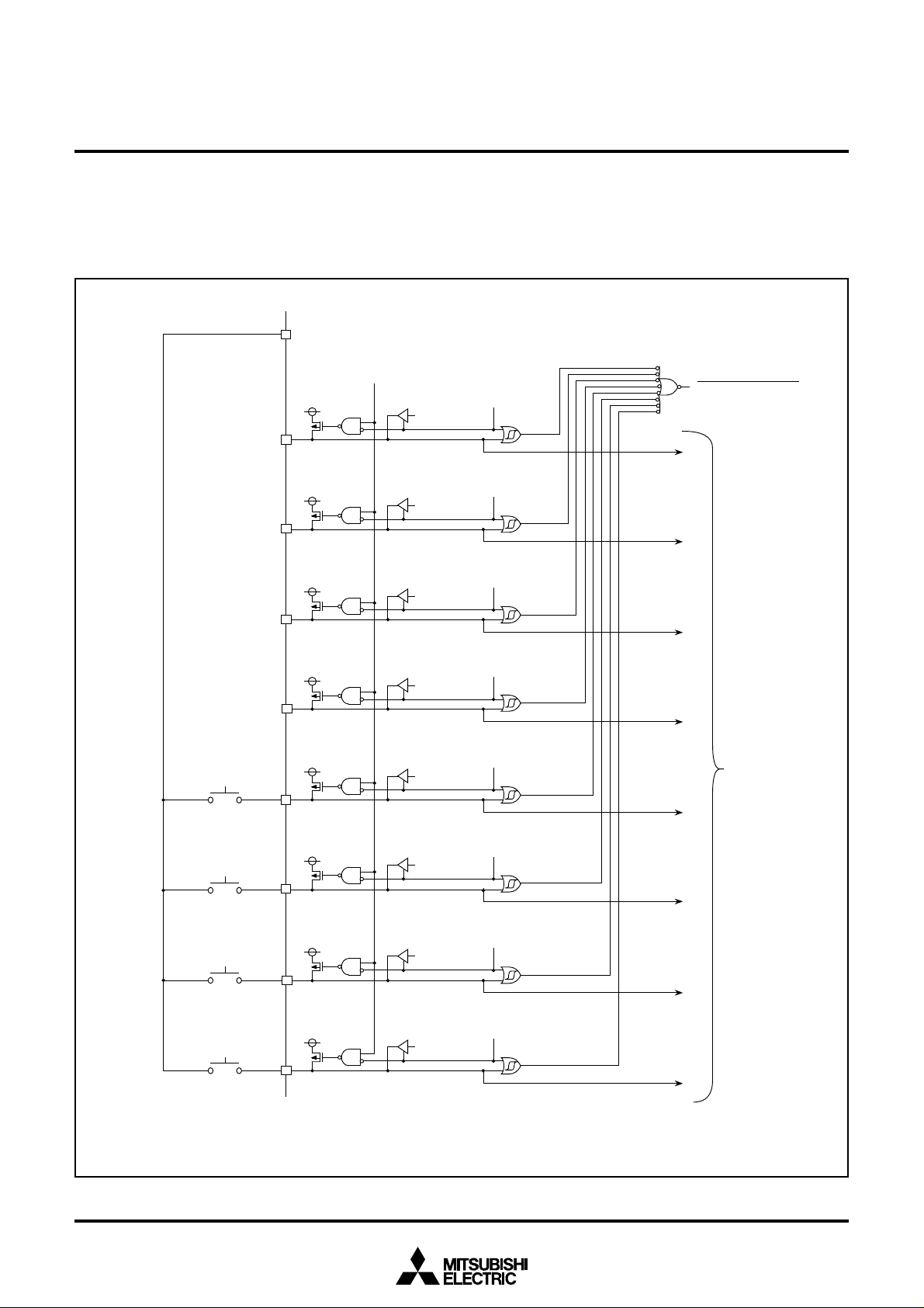
Key Input Interrupt (Key-on Wake-Up)
A key input interrupt request is generated by applying “L” level to any
pin of port P8 that have been set to input mode. In other words, it is
generated when AND of input level goes from “1” to “0”. An example
Port PXx
“L” level output
PULL register A
Bit 5 = “1”
P8
P8
P8
7
output
6
output
5
output
✽
✽
✽ ✽
✽ ✽
✽ ✽✽
Port P8
latch
Port P8
latch
Port P8
latch
of using a key input interrupt is shown in Figure 15, where an interrupt request is generated by pressing one of the keys consisted as
an active-low key matrix which inputs to ports P8
Port P8
direction register = “1”
7
6
5
7
Port P8
direction register = “1”
6
5
Port P8
direction register = “1”
0–P83.
Key input interrupt request
P8
4
output
P8
P8
P8
P8
3
input
2
input
1
input
0
input
4
Port P8
✽ ✽✽
Port P8
latch
✽ ✽✽
Port P8
latch
✽ ✽✽
Port P8
latch
✽ ✽✽
Port P8
latch
✽
✽ ✽
Port P8
latch
direction register = “1”
4
Port P8
3
direction register = “0”
3
Port P8
2
direction register = “0”
2
Port P8
1
direction register = “0”
1
0
Port P8
direction register = “0”
0
Port P8
Input reading circuit
Fig. 15 Connection example when using key input interrupt and port P8 block diagram
18
✽ P-channel transistor for pull-up
✽ ✽ CMOS output buffer
TIMERS
8-Bit Timer
The 38C3 group has six built-in timers : Timer 1, Timer 2, Timer 3,
Timer 4, Timer 5, and Timer 6.
Each timer has the 8-bit timer latch. All timers are down-counters.
When the timer reaches “00
count pulse. Then the contents of the timer latch is reloaded into the
timer and the timer continues down-counting. When a timer
underflows, the interrupt request bit corresponding to that timer is
set to “1.”
The count can be stopped by setting the stop bit of each timer to “1.”
The system clock φ can be set to either the high-speed mode or lowspeed mode with the CPU mode register. At the same time, timer
internal count source is switched to either f(X
●Timer 1, Timer 2
The count sources of timer 1 and timer 2 can be selected by setting
the timer 12 mode register. A rectangular waveform of timer 1 underflow signal divided by 2 is output from the P4
form polarity changes each time timer 1 overflows. The active edge
of the external clock CNTR
interrupt edge selection register.
At reset or when executing the STP instruction, all bits of the timer 12
mode register are cleared to “0,” timer 1 is set to “FF
set to “01
16.”
●Timer 3, Timer 4
The count sources of timer 3 and timer 4 can be selected by setting
the timer 34 mode register. A rectangular waveform of timer 3 underflow signal divided by 2 is output from the P4
form polarity changes each time timer 3 overflows. The active edge
of the external clock CNTR
interrupt edge selection register.
●Timer 5, Timer 6
The count sources of timer 5 and timer 6 can be selected by setting
the timer 56 mode register. A rectangular waveform of timer 6 underflow signal divided by 2 can be output from the P5
●Timer 6 PWM1 Mode
Timer 6 can output a rectangular waveform with “H” duty cycle n/
(n+m) from the P5
2/PWM1 pin by setting the timer 56 mode register
(refer to Figure 17). The n is the value set in timer 6 latch (address
16) and m is the value in the timer 6 PWM register (address
0025
0027
16). If n is “0,” the PWM output is “L,” if m is “0,” the PWM output
is “H” (n = 0 is prior than m = 0). In the PWM mode, interrupts occur
at the rising edge of the PWM output.
16,” an underflow occurs with the next
IN) or f(XCIN).
1/T1OUT pin. The wave-
0 can be switched with the bit 6 of the
16,” and timer 2 is
2/T3OUT pin. The wave-
1 can be switched with the bit 7 of the
2/PWM1 pin.
MITSUBISHI MICROCOMPUTERS
38C3 Group
SINGLE-CHIP 8-BIT CMOS MICROCOMPUTER
b7
b7
b7
b0
Timer 12 mode register
(T12M: address 0028
Timer 1 count stop bit
0 : Count operation
1 : Count stop
Timer 2 count stop bit
0 : Count operation
1 : Count stop
Timer 1 count source selection bits
00 : f(X
IN
01 : f(X
CIN
10 : f(X
IN
11 : f(X
IN
Timer 2 count source selection bits
00 : Underflow of Timer 1
01 : f(X
CIN
10 : External count input CNTR
11 : Not available
Timer 1 output selection bit (P4
0 : I/O port
1 : Timer 1 output
Not used (returns “0” when read)
(Do not write “1” to this bit.)
b0
Timer 34 mode register
(T34M: address 0029
Timer 3 count stop bit
0 : Count operation
1 : Count stop
Timer 4 count stop bit
0 : Count operation
1 : Count stop
Timer 3 count source selection bits
00 : f(X
01 : Underflow of Timer 2
10 : f(X
11 : f(X
Timer 4 count source selection bits
00 : f(X
01 : Underflow of Timer 3
10 : External count input CNTR
11 : Not available
Timer 3 output selection bit (P4
0 : I/O port
1 : Timer 3 output
Not used (returns “0” when read)
(Do not write “1” to this bit.)
b0
Timer 56 mode register
(T56M: address 002A
Timer 5 count stop bit
0 : Count operation
1 : Count stop
Timer 6 count stop bit
0 : Count operation
1 : Count stop
Timer 5 count source selection bit
0 : f(X
IN
1 : Underflow of Timer 4
Timer 6 operation mode selection bit
0 : Timer mode
1 : PWM mode
Timer 6 count source selection bits
00 : f(X
01 : Underflow of Timer 5
10 : Underflow of Timer 4
11 : Not available
Timer 6 (PWM) output selection bit (P5
0 : I/O port
1 : Timer 6 output
Not used (returns “0” when read)
(Do not write “1” to this bit.)
)/16 or f(X
)
)/32 or f(X
)/128 or f(X
)
IN
)/16 or f(X
IN
)/32 or f(X
IN
)/128 or f(X
IN
)/16 or f(X
)/16 or f(X
IN
)/16 or f(X
16
)
CIN
)/16
CIN
)/32
CIN
)/128
16
)
CIN
)/16
CIN
)/32
CIN
)/128
CIN
)/16
16
)
CIN
)/16
CIN
)/16
0
1
)
1
2
)
2
)
Fig. 16 Structure of Timer Related Register
19

X
P41/T1
OUT
P53/CNTR
MITSUBISHI MICROCOMPUTERS
38C3 Group
SINGLE-CHIP 8-BIT CMOS MICROCOMPUTER
Data bus
CIN
1/2
Internal system clock
“1”
X
IN
selection bit
“0”
1/16
1/32
1/128
1
latch
P4
Timer 1 count source
“01”
selection bit
“00”
“10”
“11”
Timer 1 count
stop bit
Timer 1 latch (8)
Timer 1 (8)
FF
16
1/2
Timer 1 output selection bit
Timer 2 count source
“00”
1
direction register
P4
selection bit
“01”
“10”
0
Rising/Falling
active edge switch
Timer 2 count
stop bit
Timer 2 latch (8)
Timer 2 (8)
01
16
RESET
STP instruction
Timer 1 interrupt request
Timer 2 interrupt request
P42/T3
P54/CNTR
OUT
Timer 3 count
stop bit
Timer 4 count
stop bit
Timer 5 count
stop bit
Timer 6 count
stop bit
Timer 3 latch (8)
Timer 3 (8)
Timer 4 latch (8)
Timer 4 (8)
Timer 5 latch (8)
Timer 5 (8)
Timer 6 latch (8)
Timer 6 (8)
Timer 3 interrupt request
Timer 4 interrupt request
CNTR1 interrupt request
Timer 5 interrupt request
Timer 6 interrupt request
Timer 3 count source
selection bit
“01”
“00”
2
latch
P4
1/2
Timer 3 output selection bit
2
direction register
P4
“10”
“11”
Timer 4 count source
“01”
selection bit
“00”
“10”
1
Rising/Falling
active edge switch
Timer 5 count source
selection bit
“1”
“0”
Timer 6 count source
“01”
selection bit
“00”
“10”
P52/PWM
Fig. 17 Block diagram of timer
20
Timer 6 PWM register (8)
2
latch
1
P5
Timer 6 output selection bit
2
direction register
P5
“1”
“0”
Timer 6 operation
mode selection bit
PWM
1/2

Timer 6
count source
Timer 6
PWM mode
t
s
n ✕ ts m ✕ ts
(n+m) ✕ ts
MITSUBISHI MICROCOMPUTERS
38C3 Group
SINGLE-CHIP 8-BIT CMOS MICROCOMPUTER
Timer 6 interrupt request Timer 6 interrupt request
Note: PWM waveform (duty : n/(n+m) and period : (n+m) ✕ ts) is output.
n: setting value of Timer 6
m: setting value of Timer 6 PWM register
ts: period of Timer 6 count source
Fig. 18 Timing chart of timer 6 PWM1 mode
16-bit Timer
Timer A is a 16-bit timer that can be selected in one of four modes by
the timer A mode register and the timer A control register.
●Timer A
The timer A operates as down-count. When the timer contents reach
“0000
16”, an underflow occurs at the next count pulse and the timer
latch contents are reloaded. After that, the timer continues countdown. When the timer underflows, the interrupt request bit corresponding to the timer A is set to “1”.
(1) Timer mode
The count source can be selected by setting the timer A mode register.
(2) Pulse output mode
Pulses of which polarity is inverted each time the timer underflows
are output from the TA
just as in the timer mode.
When using this mode, set port P5
mode.
OUT pin. Except for that, this mode operates
0 sharing the TAOUT pin to output
types of delay time by a delay circuit.
When using this mode, set port P5
mode and set port P5
It is possible to force the timer A output to be “L” using pins INT
INT
2 by the timer A control register.
0 sharing the TAOUT pin to output mode.
5 sharing the INT0 pin to input
1 and
(4) PWM mode
IGBT dummy output, an external trigger with the INT0 pin and output
control with pins INT
mode operates just as in the IGBT output mode.
The period of PWM waveform is specified by the timer A set value.
The “H” term is specified by the compare register set value.
When using this mode, set port P5
mode.
1 and INT2 are not used. Except for those, this
0 sharing the TAOUT pin to output
(3) IGBT output mode
After dummy output from the TAOUT pin, count starts with the INT0
pin input as a trigger. When the trigger is detected or the timer A
underflows, “H” is output from the the T A
When the count value corresponds with the compare register value,
the TA
OUT output becomes “L”. When the INT0 signal becomes “H”,
the T A
OUT output is forced to become “L”.
After noise is cleared by noise filters, judging continuous 4-time same
levels with sampling clocks to be signals, the INT
OUT pin.
0 signal can use 4
21

P50/TA
INT
0
Noise filter sampling
clock selection bit
X
IN
INT
1
INT
2
OUT
(Note)
Note: The initial value of M version becomes “1” (output).
Noise filter
(4-time same levels judgement)
1/2
1/4
Divider
1/1
1/2
1/4
Divider
1/8
“1”
“0”
“1”
“0”
P50
direction
register
Output selection bit
Timer A count
source selection bit
TA
OUT
output
control bit 1
OUT
output
TA
control bit 2
P5
0
latch
0µs
4/f(XIN)
8/f(XIN)
16/f(X
IN
Delay circuit
Timer A
operating
mode bits
Timer A operating
mode bits
“10”
“10”
“00”, “01”, “11”
Timer A (high-order) latch (8)
Timer A (high-order) (8)
Compare register (high-order) (8)
“00”, “01”, “11”
IGBT output mode
PWM mode
TA
edge switch bit
External trigger delay
time selection bit
“00”
01
”
“
“
10
”
)
11
”
“
Internal trigger start
Timer A (low-order) latch (8)
Compare register (low-order) (8)
TA
OUT
active
edge switch bit
“0”
R
S
Q
“1”
“0”
“1”
OUT
active
D
Q
Pulse output mode
S
S
Q
T
Q
MITSUBISHI MICROCOMPUTERS
38C3 Group
SINGLE-CHIP 8-BIT CMOS MICROCOMPUTER
Data bus
Timer A write control bit
Timer A (low-order) (8)
Timer A start
signal
Match
Timer A underflow
interrupt request
Fig. 19 Block diagram of timer A
b7 b0
Timer A mode register
(TAM : address 0030
Timer A operating mode bits
00 : Timer mode
01 : Pulse output mode
10 : IGBT output mode
11 : PWM mode
Timer A write control bit
0 : Write data to both timer latch and timer
1 : Write data to timer latch onl
Timer A count source selection bits
0 0 : f(X
0 1 : f(X
1 0 : f(X
1 1 : f(X
IN)
IN)/2
IN)/4
IN)/8
Timer A output active edge switch bit
0 : Output starts with “L” level
1 : Output starts with “H” level
Timer A count stop bit
0 : Count operating
1 : Count stop
Timer A output selection bit (P5
0 : I/O port
1 : Timer A output
Fig. 20 Structure of timer A related registers
16)
b7 b0
Timer A control register
(TACON : address 0031
16)
Noise filter sampling clock selection bit
IN)/2
0 : f(X
1 : f(X
IN)/4
External trigger delay time selection bits
0 0 : No delay
0 1 : ( 4/f(X
1 0 : ( 8/f(X
y
1 1 : (16/f(X
Timer A output control bit 1 (P5
IN))µs
IN))µs
IN))µs
6)
0 : Not used
1 : INT1 interrupt used
Timer A output control bit 2 (P5
7)
0 : Not used
1 : INT2 interrupt used
Not used (returns “0” when read)
0)
22

Timer A count
source
Timer A
PWM mode
IGBT output mode
Note: PWM waveform (duty : (n-m+1)/(n+1) and period : (n+1) ✕ ts) is output.
n : setting value of Timer A
m : setting value of compare register
ts : period of Timer A count source
t
s
(n-m+1) ✕ ts m ✕ ts
(n+1) ✕ ts
MITSUBISHI MICROCOMPUTERS
38C3 Group
SINGLE-CHIP 8-BIT CMOS MICROCOMPUTER
Fig. 21 Timing chart of timer A PWM, IGBT output modes
■Notes on Timer A
(1) Write order to timer A
• In the timer and pulse output modes, write to the timer A register
(low-order) first and to the timer A register (high-order) next. Do not
write to only one side.
• In the IGBT and PWM modes, write to the registers as follows:
the compare register (high- and low-order)
the timer A register (low-order)
the timer A register (high-order).
It is possible to use whichever order to write to the compare register
(high- and low-order). However, write both the compare register and
the timer A register at the same time.
(2) Read order to timer A
• In all modes, read to the timer A register (high-order) first and to the
timer A register (low-order) next. Read order to the compare register is not specified.
• If reading to the timer A register during write operation or writing to
it during read operation, normal operation will not be performed.
(3) Write to timer A
• When writing a value to the timer A address to write to the latch
only, the value is set into the reload latch and the timer is updated
at the next underflow. Normally, when writing a value to the timer A
address, the value is set into the timer and the timer latch at the
same time, because they are written at the same time.
When writing to the latch only, if the write timing to the high-order
reload latch and the underflow timing are almost the same, an expected value may be set in the high-order counter.
• Do not switch the timer count source during timer count operation.
Stop the timer count before switching it. Additionally, when performing write to the latch and the timer at the same time, the timer count
value may change large.
(4) Set of timer A mode register
Set the write control bit to “1” (write to the latch only) when setting the
IGBT and PWM modes.
Output waveform simultaneously reflects the contents of both registers at the next underflow after writing to the timer A register (highorder).
(5) Output control function of timer A
When using the output control function (INT
mode, set the levels of INT
or to “L” in the rising edge active before switching to the IGBT mode.
1 and INT2 to “H” in the falling edge active
1 and INT2) in the IGBT
23

MITSUBISHI MICROCOMPUTERS
38C3 Group
SINGLE-CHIP 8-BIT CMOS MICROCOMPUTER
SERIAL I/O
The 38C3 group has a built-in 8-bit clock synchronous serial I/O. The
XCIN
XIN
P47/SRDY
P46/SCLK1
P45/SOUT
P44/SIN
P40/SCLK2
Internal
system clock
“1”
selection bit
“0”
Serial I/O port selection bit
Serial I/O port selection bit
P47 latch
“0”
“1”
SRDY output selection bit
6 latch
P4
“0”
“1”
5 latch
P4
“0”
“1”
P40 latch
“0”
Serial I/O port selection bit
“1”
SRDY
Synchronous clock
selection bit
Synchronous
circuit
SCLK
External clock
I/O pins of serial I/O also operate as I/O port P4, and their function is
selected by the serial I/O control register 1 (address 001916).
Internal synchronous
clock selection bits
1/8
1/16
1/32
1/64
Divider
1/128
1/256
“1”
“0”
Serial I/O counter (3)
Serial I/O shift register (8)
Data bus
Serial I/O
interrupt request
Fig. 22 Block diagram of serial I/O
24

MITSUBISHI MICROCOMPUTERS
Serial I/O control register 1
(SIOCON1 : address 0019
16
)
Internal synchronous clock selection bits
b2 b1 b0
0 0 0 : f(X
IN
)/8 or f(X
CIN
)/8
0 0 1 : f(X
IN
)/16 or f(X
CIN
)/16
0 1 0 : f(X
IN
)32 or f(X
CIN
)/32
0 1 1 : f(X
IN
)/64 or f(X
CIN
)/64
1 1 0 : f(X
IN
)/128 or f(X
CIN
)/128
1 1 1 : f(X
IN
)/256 or f(X
CIN
)/256
Serial I/O port selection bit (P4
0
, P45, P46)
0 : I/O port
1 : S
OUT
, S
CLK1
, S
CLK2
signal pin
S
RDY
output selection bit (P47)
0 : I/O port
1 : S
RDY
signal pin
Transfer direction selection bit
0 : LSB first
1 : MSB first
Synchronous clock selection bit
0 : External clock
1 : Internal clock
P-channel output disable bit (P4
0
, P45, P46)
0 : CMOS output (in output mode)
1 : N-channel open-drain (in output mode)
b7 b0
Serial I/O control register 2
(SIOCON2: address 001A
16
)
Synchronous clock output pin selection bit
0 : S
CLK1
1 : S
CLK2
Not used (returns “0” when read)
b7 b0
38C3 Group
SINGLE-CHIP 8-BIT CMOS MICROCOMPUTER
[Serial I/O Control Registers 1, 2 (SIOCON1,
SIOCON2)] 0019
Each of the serial I/O control registers 1, 2 contains 8 bits that select
various control parameters of serial I/O.
●Operation in serial I/O mode
Either an internal clock or an external clock can be selected as the
synchronous clock for serial I/O transfer. A dedicated divider is builtin as the internal clock, giving a choice of six clocks.
16, 001A16
When internal clock is selected, serial I/O starts to transfer by a write
signal to the serial I/O register (address 001B
been transferred, the S
OUT pin goes to high impedance.
16). After 8 bits have
When external clock is selected, the clock must be controlled externally because the contents of the serial I/O register continue to shift
while the transfer clock is input. In this case, the S
OUT pin does not
go to high impedance at the completion of data transfer.
The interrupt request bit is set at the end of the transfer of 8 bits,
regardless of whether the internal or external clock is selected.
Fig. 23 Structure of serial I/O control register
Synchronous clock
Serial I/O register
write signal
Serial I/O output
S
Receive enable signal
S
Note: When internal clock is selected, the S
transfer ends.
Fig. 24 Serial I/O timing (for LSB first)
Transfer clock
OUT
Serial I/O input
S
IN
RDY
D
0
D1D
OUT
pin goes to high impedance after
2
D
3
D
4
(Note)
D
5
D
6
D
7
Interrupt request bit set
25

MITSUBISHI MICROCOMPUTERS
38C3 Group
SINGLE-CHIP 8-BIT CMOS MICROCOMPUTER
A-D CONVERTER
The 38C3 group has a 10-bit A-D converter. The A-D converter performs successive approximation conversion.
[A-D Conversion Register (AD)] 003316, 003416
One of these registers is a high-order register, and the other is a loworder register. The high-order 8 bits of a conversion result is stored in
the A-D conversion register (high-order) (address 0034
16), and the
low-order 2 bits of the same result are stored in bit 7 and bit 6 of the
A-D conversion register (low-order) (address 0033
16).
During A-D conversion, do not read these registers.
[A-D Control Register (ADCON)] 003216
This register controls A-D converter. Bits 2 to 0 are analog input pin
selection bits. Bit 4 is an AD conversion completion bit and “0” during
A-D conversion. This bit is set to “1” upon completion of A-D conversion.
A-D conversion is started by setting “0” in this bit.
[Comparison V oltage Generator]
The comparison voltage generator divides the voltage between A V SS
and VREF, and outputs the divided voltages.
[Channel Selector]
The channel selector selects one of the input ports P67/AN7–P60/
AN0 and inputs it to the comparator.
Note that the comparator is constructed linked to a capacitor, so set
f(XIN) to at least 500 kHz during A-D conversion. Use a CPU system
clock dividing the main clock X
b7 b0
b7
IN as the internal system clock.
A-D control register
(ADCON: address 0032
Analog input pin selection bits
000: P6
0
/AN
001: P61/AN
010: P62/AN
011: P63/AN
100: P64/AN
101: P65/AN
110: P66/AN
111: P67/AN
Not used (returns “0” when read)
AD conversion completion bit
0: Conversion in progress
1: Conversion completed
Not used (returns “0” when read)
b0
A-D conversion register (high-order)
(ADH: address 0034
AD conversion result stored bits
16
)
0
1
2
3
4
5
6
7
16
)
[Comparator and Control Circuit]
The comparator and control circuit compares an analog input voltage with the comparison voltage and stores the result in the A-D
conversion register. When an A-D conversion is completed, the control circuit sets the AD conversion completion bit and the AD conversion interrupt request bit to “1.”
Data bus
A-D control register
P6
0
/AN
0
P61/AN
1
P62/AN
2
P63/AN
3
P64/AN
4
P65/AN
5
P66/AN
6
P67/AN
7
b7 b0
3
A-D control circuit
Comparator
Channel selector
b7
Fig. 25 Structure of A-D control register
A-D conversion register (H)
(Address 003416)
A-D conversion register (L)
(Address 0033
Resistor ladder
b0
A-D conversion register (low-order)
(ADL: address 0033
Not used (returns “0” when read)
AD conversion result stored bits
A-D interrupt request
16
)
16
)
Fig. 26 Block diagram of A-D converter
26
AV
SS
V
REF

MITSUBISHI MICROCOMPUTERS
38C3 Group
SINGLE-CHIP 8-BIT CMOS MICROCOMPUTER
LCD DRIVE CONTROL CIRCUIT
The 38C3 group has the built-in Liquid Crystal Display (LCD) drive
control circuit consisting of the following.
• LCD display RAM
• Segment output enable register
• LCD mode register
• Selector
• Timing controller
• Common driver
• Segment driver
• Bias control circuit
A maximum of 32 segment output pins and 4 common output pins
can be used.
Up to 128 pixels can be controlled for a LCD display. When the LCD
enable bit is set to “1” after data is set in the LCD mode register, the
b7 b0
b7 b0
Note : LCDCK is a clock for a LCD timing controller.
Segment output enable register
(SEG : address 0038
LCD mode register
(LM : address 0039
segment output enable register, and the LCD display RAM, the LCD
drive control circuit starts reading the display data automatically , performs the bias control and the duty ratio control, and displays the
data on the LCD panel.
Table 7 Maximum number of display pixels at each duty ratio
Duty ratio
1
2
3
4
16
)
Segment output enable bit 0
0 : I/O ports P2
1 : Segment output SEG0–SEG
Segment output enable bit 1
0 : I/O ports P2
1 : Segment output SEG4–SEG
Segment output enable bit 2
0 : I/O ports P0
1 : Segment output SEG8–SEG
Segment output enable bit 3
0 : I/O ports P0
1 : Segment output SEG12–SEG
Segment output enable bit 4
0 : I/O ports P1
1 : Segment output SEG16–SEG
Segment output enable bit 5
0 : I/O ports P1
1 : Segment output SEG20–SEG
Segment output enable bit 6
0 : Output ports P3
1 : Segment output SEG24–SEG
Segment output enable bit 7
0 : Output ports P3
1 : Segment output SEG28–SEG
Duty ratio selection bits
0 0 : 1 (use COM
0 1 : 2 (use COM
1 0 : 3 (use COM
1 1 : 4 (use COM
Bias control bit
0 : 1/3 bias
1 : 1/2 bias
LCD enable bit
0 : LCD OFF
1 : LCD ON
Not used (returns “0” when read)
(Do not write “1” to this bit.)
LCD circuit divider division ratio selection bits
0 0 : Clock input
0 1 : 2 division of clock input
1 0 : 4 division of clock input
1 1 : 8 division of clock input
LCDCK count source selection bit (Note)
0 : f(X
1 : f(X
CIN
)/32
IN
)/8192 (f(X
0
–P2
3
4
–P2
7
0
–P0
3
4
–P0
7
0
–P1
3
4
–P1
7
0
–P3
3
4
–P3
7
16
)
0
)
0
,COM1)
0
–COM2)
0
–COM3)
CIN
)/8192 in low-speed mode)
Maximum number of display pixels
32 dots
or 8 segment LCD 4 digits
64 dots
or 8 segment LCD 8 digits
96 dots
or 8 segment LCD 12 digits
128 dots
or 8 segment LCD 16 digits
3
7
11
15
19
23
27
31
Fig. 27 Structure of LCD related registers
27

Data bus
Timing controller
LCD
divider
f(X
CIN
)/32
f(X
IN
)/8192
(f(X
CIN
)/8192 in low-speed mode)
Common
driver
Bias control
COM
0
COM
1
COM
2
COM
3
V
SS
V
L1
V
L2
V
L3
P2
3
/SEG
3
P2
2
/SEG
2
P2
1
/SEG
1
P2
0
/SEG
0
Address 0040
16
Address 0041
16
“1”
“0”
LCDCK
LCDCK count source
selection bit
LCD circuit
divider division
ratio selection bits
Bias control bit
LCD enable bit
Duty ratio selection bits
2
2
Selector Selector Selector Selector
Selector
Selector
LCD display RAM
Address 004F
16
P3
6
/SEG
30
P0
4
/SEG
12
P3
7
/SEG
31
Segment
driver
Segment
driver
Segment
driver
Segment
driver
Segment
driver
Segment
driver
Common
driver
Common
driver
Common
driver
MITSUBISHI MICROCOMPUTERS
38C3 Group
SINGLE-CHIP 8-BIT CMOS MICROCOMPUTER
Fig. 28 Block diagram of LCD controller/driver
28

MITSUBISHI MICROCOMPUTERS
38C3 Group
SINGLE-CHIP 8-BIT CMOS MICROCOMPUTER
Bias Control and Applied Voltage to LCD Power Input Pins
T o the LCD power input pins (VL1–VL3), apply the voltage value shown
in Table 8 according to the bias value.
Select a bias value by the bias control bit (bit 2 of the LCD mode
register).
Common Pin and Duty Ratio Control
The common pins (COM0–COM3) to be used are determined by duty
ratio.
Select duty ratio by the duty ratio selection bits (bits 0 and 1 of the
LCD mode register).
When selecting 1-duty ratio, 1/1 bias can be used.
Table 8 Bias control and applied voltage to VL1–VL3
Bias value
Voltage value
VL3=VLCD
1/3 bias
VL2=2/3 VLCD
VL1=1/3 VLCD
1/2 bias
1/1 bias
(1-duty ratio)
Note 1: VLCD is the maximum value of supplied voltage for the LCD panel.
VL3=VLCD
VL2=VL1=1/2 VLCD
VL3=VLCD
VL2=VL1=VSS
Table 9 Duty ratio control and common pins used
Duty ratio selection bit
Duty
ratio
Notes 1:COM1, COM2, and COM3 are open.
1
2
3
4
Bit 1
0
0
1
1
2 and COM3 are open.
2:COM
3 is open.
3:COM
Bit 0
0
1
0
1
Common pins used
COM0 (Note 1)
COM0, COM1 (Note 2)
COM0–COM2 (Note 3)
COM0–COM3
Contrast control
V
L3
V
L2
V
L1
1/3 bias
R1 = R2 = R3
Fig. 29 Example of circuit at each bias
R1
R2
R3
1/2 bias
Contrast control
V
L3
V
L2
V
L1
R4 = R5
R4
R5
1/1 bias
Contrast control
V
L3
V
L2
V
L1
R6
29

MITSUBISHI MICROCOMPUTERS
38C3 Group
SINGLE-CHIP 8-BIT CMOS MICROCOMPUTER
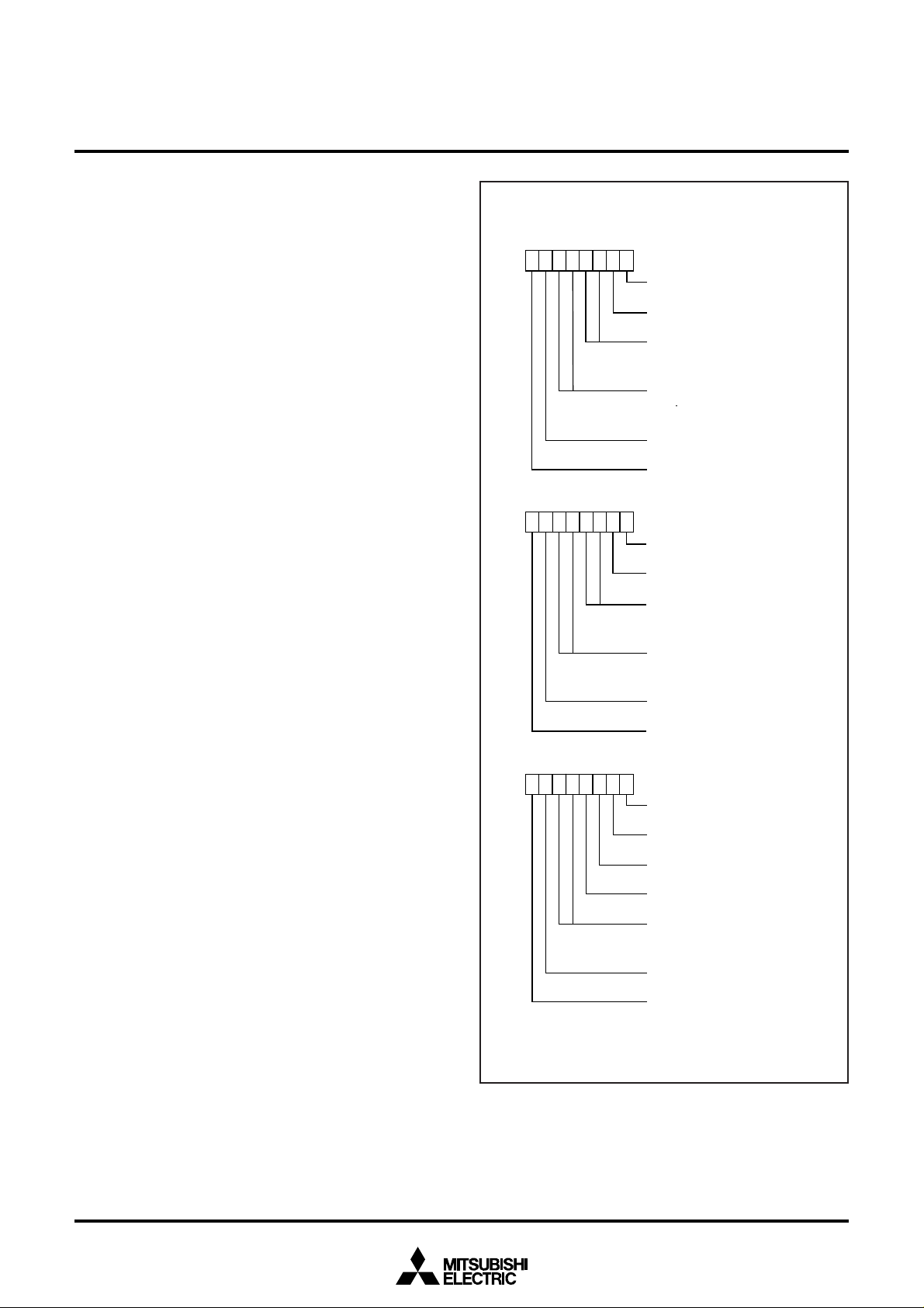
LCD Display RAM
Address 004016 to 004F16 is the designated RAM for the LCD display . When “1” are written to these addresses, the corresponding segments of the LCD display panel are turned on.
Bit
Address
004016
004116
004216
004316
004416
004516
004616
004716
004816
004916
004A16
004B16
004C16
004D16
004E16
004F16
76543210
SEG1
SEG3
SEG5
SEG7
SEG9
SEG11
SEG13
SEG15
SEG17
SEG19
SEG21
SEG23
SEG25
SEG27
SEG29
SEG31
COM3 COM0COM2 COM1 COM0 COM3 COM2 COM1
LCD Drive Timing
The LCDCK timing frequency (LCD drive timing) is generated internally and the frame frequency can be determined with the following
equation;
(frequency of count source for LCDCK)
f(LCDCK)=
(divider division ratio for LCD)
f(LCDCK)
Frame frequency=
duty ratio
SEG0
SEG2
SEG4
SEG6
SEG8
SEG10
SEG12
SEG14
SEG16
SEG18
SEG20
SEG22
SEG24
SEG26
SEG28
SEG30
Fig. 30 LCD display RAM map
30

MITSUBISHI MICROCOMPUTERS
SINGLE-CHIP 8-BIT CMOS MICROCOMPUTER
Internal
signal
LCDCK
timing
1/4 duty Voltage level
V
L3
COM
COM
COM
COM
SEG
1/3 duty
COM
COM
0
1
2
3
0
OFF ON OFF ON
COM
3
COM2COM1COM
0
1
COM
0
3
COM2COM1COM
0
VL2=V
V
SS
V
L3
V
SS
V
L3
VL2=V
V
SS
38C3 Group
L1
L1
COM
2
SEG
0
COM0COM2COM
1/2 duty
COM
0
COM
1
SEG
0
COM1COM0COM
1/1 duty (1/1 bias)
0
COM
SEG
0
OFFON ON OFF ON OFF
COM
1
0
COM2COM1COM0COM
OFFON OFFON OFFON OFFON
COM
1
0
COM1COM0COM1COM
ONOFF
V
L3
V
SS
2
V
L3
VL2=V
L1
V
SS
V
L3
V
SS
0
V
L3
VL2=VL1=V
V
V
SS
L3
SS
Fig. 31 LCD drive waveform (1/2 bias)
31

Internal signal
LCDCK timing
MITSUBISHI MICROCOMPUTERS
38C3 Group
SINGLE-CHIP 8-BIT CMOS MICROCOMPUTER
1/4 duty
COM
COM
COM
COM
SEG
1/3 duty
COM
COM
COM
Voltage level
V
L3
V
0
1
2
3
0
L2
V
L1
V
SS
V
L3
V
SS
OFF ON OFF ON
COM
3
COM2COM
0
1
2
1
COM
COM
0
3
COM
2
COM
1
COM
0
V
L3
V
L2
V
L1
V
SS
SEG
0
COM
0
1/2 duty
COM
0
COM
1
SEG
0
COM1COM
Fig. 32 LCD drive waveform (1/3 bias)
OFFON ON OFF ON OFF
COM2COM
1
COM
COM2COM
0
1
COM
0
COM
OFFON OFFON OFFON OFFON
0
COM
1
COM
COM1COM
0
0
COM
1
COM
V
L3
V
SS
2
V
L3
V
L2
V
L1
V
SS
V
L3
V
SS
0
32

φ CLOCK OUTPUT FUNCTION
The internal system clock φ can be output from port P43 by setting
the φ output control register. Set “1” to bit 3 of the port P4 direction
register when outputting φ clock.
b7 b0
SINGLE-CHIP 8-BIT CMOS MICROCOMPUTER
φ output control register
(CKOUT : address 002B
φ output control bit
0 : Port function
1 : φ clock output
Not used (return “0” when read)
16)
MITSUBISHI MICROCOMPUTERS
38C3 Group
Fig. 33 Structure of φ output control register
33

ROM CORRECTION FUNCTION
The 38C3 group has the ROM correction function correcting data at
the arbitrary addresses in the ROM area.
[ROM correct address register] 0F0216 – 0F1116
This is the register to store the address performing ROM correction.
There are two types of registers to correct up to 8 addresses: one is
the register to store the high-order address and the other is to store
the low-order address.
[ROM correct enable register (RC1)] 0F0116
This is the register to enable the ROM correction function. When setting the bit corresponding to the ROM correction address to “1”, the
ROM correction function is enabled.
It becomes invalid to the addresses of which corresponding bit is “0”.
All bits are “0” at the initial state.
MITSUBISHI MICROCOMPUTERS
38C3 Group
SINGLE-CHIP 8-BIT CMOS MICROCOMPUTER
ROM correct high-order address register 1
0F02
16
ROM correct low-order address register 1
0F03
16
ROM correct high-order address register 2
0F04
16
ROM correct low-order address register 2
0F05
16
ROM correct high-order address register 3
0F06
16
ROM correct low-order address register 3
0F07
16
ROM correct high-order address register 4
0F08
16
ROM correct low-order address register 4
0F09
16
ROM correct high-order address register 5
0F0A
16
ROM correct low-order address register 5
0F0B
16
ROM correct high-order address register 6
0F0C
16
ROM correct low-order address register 6
0F0D
16
ROM correct high-order address register 7
0F0E
16
ROM correct low-order address register 7
0F0F
16
ROM correct high-order address register 8
0F10
16
0F11
16
ROM correct low-order address register 8
[ROM correct data]
This is the register to store a correct data for the address specified by
the ROM correct address register.
■Notes on ROM correction function
1.To use the ROM correction function, transfer data to each ROM
correct data register in the initial setting.
2. Do not specify the same addresses in the ROM correct address
register.
b7 b0
Fig. 36 Structure of ROM correct enable register 1
Fig. 34 Structure of ROM correct address register
0050
0051
0052
0053
0054
0055
0056
0057
16
16
16
16
16
16
16
16
ROM correct data 1
ROM correct data 2
ROM correct data 3
ROM correct data 4
ROM correct data 5
ROM correct data 6
ROM correct data 7
ROM correct data 8
Fig. 35 Structure of ROM correct data
ROM correct enable register 1(address 0F0116)
RC1
ROM correct address 1 enable bit
0 : Disabled
1 : Enabled
ROM correct address 2 enable bit
0 : Disabled
1 : Enabled
ROM correct address 3 enable bit
0 : Disabled
1 : Enabled
ROM correct address 4 enable bit
0 : Disabled
1 : Enabled
ROM correct address 5 enable bit
0 : Disabled
1 : Enabled
ROM correct address 6 enable bit
0 : Disabled
1 : Enabled
ROM correct address 7 enable bit
0 : Disabled
1 : Enabled
ROM correct address 8 enable bit
0 : Disabled
1 : Enabled
34

MITSUBISHI MICROCOMPUTERS
38C3 Group
SINGLE-CHIP 8-BIT CMOS MICROCOMPUTER
RESET CIRCUIT
T o reset the microcomputer, RESET pin should be held at an “L” level
for 2 µs or more. Then the RESET pin is returned to an “H” level (the
power source voltage should be between 2.5 V and 5.5 V, and the
oscillation should be stable), reset is released. After the reset is completed, the program starts from the address contained in address
FFFD
16 (high-order byte) and address FFFC16 (low-order byte). Make
sure that the reset input voltage is less than 0.5 V for V
(switching to the high-speed mode, a power source voltage must be
between 4.0 V and 5.5 V).
CC of 2.5 V
Power source
voltage
V
RESET
RESET
CC
V
CC
Reset input
voltage
Fig. 37 Reset circuit example
Poweron
(Note)
0V
CC
0V
Note : Reset release voltage ; Vcc=2.5 V
0.2V
Power source
voltage detection
circuit
X
IN
φ
RESET
Internal
reset
Address
Data
SYNC
????
XIN : about 8000 cycles
Note
1: The frequency relation of f(XIN) and f(φ) is f(XIN) = 8 • f(φ).
2: The question marks (?) indicate an undefined state that depends on the previous state.
FFFC FFFD
ADL
Reset address from
vector table
AD
H, ADL
ADH
Fig. 38 Reset sequence
35

MITSUBISHI MICROCOMPUTERS
38C3 Group
SINGLE-CHIP 8-BIT CMOS MICROCOMPUTER
Address Register contents
(1)
Port P0
(2)
Port P0 direction register
(3)
Port P1
(4)
Port P1 direction register
Port P2
(5)
Port P2 direction register
(6)
Port P3
(7)
(8)
Port P4
(9)
Port P4 direction register
(10)
Port P5
(11)
Port P5 direction register
(12)
Port P6
(13)
Port P6 direction register
(14)
Port P7
(15)
Port P7 direction register
(16)
Port P8
(17)
Port P8 direction register
(18)
PULL register A
(19)
PULL register B
(20)
Port P8 output selection register
(21)
Serial I/O control register 1
(22)
Serial I/O control register 2
(23)
Timer 1
(24)
Timer 2
(25)
Timer 3
(26)
Timer 4
(27)
Timer 5
(28)
Timer 6
(29)
Timer 12 mode register
(30)
Timer 34 mode register
(31)
Timer 56 mode register
(32)
φ output control register
(33)
Timer A (low-order)
X: Not fixed
Since the initial values for other than above mentioned registers and RAM contents are indefinite at reset, they must be set.
In the M version, bit 0 of the port P5 direction register becomes “1.”
000016
000116
000216
000316
000416
000516
000616
000816
000916
000A16
000B16
000C16
000D16
000E16
000F16
001016
001116
001616
001716
001816
001916
001A16
002016
002116
002216
002316
002416
002516
002816
002916
002A16
002B16
002C16
0016
0016
0016
0016
0016
0016
0016
0016
0016
0016
0016
0016
0016
0016
0016
0016
0016
0F16
0016
0016
0016
0016
FF16
0116
FF16
FF16
FF16
FF16
0016
0016
0016
0016
FF16
(34)
Timer A (high-order)
(35)
Compare register (low-order)
(36)
Compare register (high-order)
Timer A mode register
(37)
(38)
Timer A control register
(39)
A-D control register
(40)
Segment output enable register
LCD mode register
(41)
(42)
Interrupt edge selection register
(43)
CPU mode register
(44)
Interrupt request register 1
(45)
Interrupt request register 2
(46)
Interrupt control register 1
(47)
Interrupt control register 2
(48)
ROM correct enable register 1
(49)
ROM correct high-order address
register 1
(50)
ROM correct low-order address
register 1
(51)
ROM correct high-order address
register 2
(52)
ROM correct low-order address
register 2
(53)
ROM correct high-order address
register 3
(54)
ROM correct low-order address
register 3
(55)
ROM correct high-order address
register 4
(56)
ROM correct low-order address
register 4
(57)
ROM correct high-order address
register 5
(58)
ROM correct low-order address
register 5
(59)
ROM correct high-order address
register 6
(60)
ROM correct low-order address
register 6
(61)
ROM correct high-order address
register 7
(62)
ROM correct low-order address
register 7
(63)
ROM correct high-order address
register 8
(64)
ROM correct low-order address
register 8
(65)
Processor status register
(66)
Program counter
Address Register contents
002D16
002E16
002F16
003016
003116
003216
003816
003916
003A
003B16
003C16
003D16
003E16
003F16
0F0116
0F0216
0F0316
0F0416
0F0516
0F0616
0F0716
0F0816
0F0916
0F0A16
0F0B16
0F0C16
0F0D16
0F0E16
0F0F16
0F1016
0F1116
(PCH)
(PCL)
16
010010 00
(PS)
FFFD16 contents
FFFC16 contents
FF16
0016
0016
0016
0016
1016
0016
0016
0016
0016
0016
0016
0016
0016
FF16
FF16
FF16
FF16
FF16
FF16
FF16
FF16
FF16
FF16
FF16
FF16
FF16
FF16
FF16
FF16
✕
✕✕✕✕✕✕
1
Fig. 39 Internal status at reset
36

MITSUBISHI MICROCOMPUTERS
38C3 Group
SINGLE-CHIP 8-BIT CMOS MICROCOMPUTER
CLOCK GENERATING CIRCUIT
The 38C3 group has two built-in oscillation circuits. An oscillation
circuit can be formed by connecting a resonator between X
X
OUT (XCIN and XCOUT). Use the circuit constants in accordance with
the resonator manufacturer's recommended values. No external resistor is needed between X
exists on-chip. However, an external feedback resistor is needed between X
CIN and XCOUT.
Immediately after power on, only the X
cillating, and X
CIN and XCOUT pins function as I/O ports.
IN and XOUT since a feedback resistor
IN oscillation circuit starts os-
IN and
Frequency control
(1) Middle-speed mode
The internal system clock is the frequency of XIN divided by 8. After
reset, this mode is selected.
(2) High-speed mode
The internal system clock is the frequency of XIN divided by 2.
(3) Low-speed mode
The internal system clock is the frequency of XCIN divided by 2.
■Notes on clock generating circuit
If you switch the mode between middle/high-speed and low-speed,
stabilize both X
for the sub clock to stabilize, especially immediately after power on
and at returning from stop mode. When switching the mode between
middle/high-speed and low-speed, set the frequency on condition
that f(X
IN and XCIN oscillations. The sufficient time is required
IN) > 3f(XCIN).
Oscillation control
(1) Stop mode
If the STP instruction is executed, the internal system clock stops at
an “H” level, and X
and timer 2 is set to “01
Either X
IN divided by 16 or XCIN divided by 16 is input to timer 1 as
count source, and the output of timer 1 is connected to timer 2. The
bits of the timer 12 mode register are cleared to “0.” Set the interrupt
enable bits of the timer 1 and timer 2 to disabled (“0”) before executing the STP instruction. Oscillator restarts when an external interrupt
is received, but the internal system clock is not supplied to the CPU
until timer 2 underflows. This allows time for the clock circuit oscillation to stabilize.
IN and XCIN oscillators stop. Timer 1 is set to “FF16”
16.”
(2) Wait mode
If the WIT instruction is executed, the internal system clock stops at
an “H” level. The states of X
before executing the WIT instruction. The internal system clock restarts at reset or when an interrupt is received. Since the oscillator
does not stop, normal operation can be started immediately after the
clock is restarted.
X
CIN
X
IN and XCIN are the same as the state
COUT XIN XOUT
Rf
Rd
C
C
CIN
Fig. 40 Ceramic resonator circuit
X
CIN XCOUT
Rf
Rd
C
C
CIN
COUT
COUT
X
IN XOUT
External oscillation circuit
CC
V
V
SS
open
C
C
IN
OUT
Fig. 41 External clock input circuit
37

XCIN
X
COUT
“1” “0”
Port XC switch bit
MITSUBISHI MICROCOMPUTERS
38C3 Group
SINGLE-CHIP 8-BIT CMOS MICROCOMPUTER
XIN
Interrupt disable flag I
Interrupt request
XOUT
Middle-/High-speed mode
SRQ
Reset
Internal system clock selection bit
Low-speed mode
“1”
Main clock stop bit
STP instruction
“0”
(Note)
1/2
1/4
High-speed mode
or Low-speed mode
WIT
instruction
Timer 1 count
source selection
bit
“1”
1/2
Main clock division ratio selection bit
Middle-speed mode
“1”
“0”
SRQ
“0”
Timer 1
SRQ
STP instruction
Timer 2 count
source selection
bit
“0”
“1”
Timing φ
(Internal system clock)
Timer 2
Note : When using the low-speed mode, set the port X
Fig. 42 Clock generating circuit block diagram
38
C switch bit to “1” .

Reset
MITSUBISHI MICROCOMPUTERS
38C3 Group
SINGLE-CHIP 8-BIT CMOS MICROCOMPUTER
Middle-speed mode
(f(φ)=1 MHz)
CM7=0(8 MHz selected)
6
=1(middle-speed)
CM
CM
5
=0(8 MHz oscillating)
4
=0(32 kHz stopped)
CM
“0”
4
CM
“1”
Middle-speed mode
((f(φ)=1 MHz)
CM
7
=0(8 MHz selected)
CM
6
=1(middle-speed)
5
=0(8 MHz oscillating)
CM
CM
4
=1(32 kHz oscillating)
“0”
7
CM
“1”
Low-speed mode
((f(φ)=16 kHz)
7
=1(32 kHz selected)
CM
CM
6
=1(middle-speed)
5
=0(8 MHz oscillating)
CM
CM
4
=1(32 kHz oscillating)
“1”
CM
“1”
4
CM
“0”
CM
6
“0”“1”
“0”
CM
“1”
6
“0”
CM
6
“0”
CM
6
“0”“1”
High-speed mode
CM
7
6
CM
CM
5
4
CM
4
“1”
High-speed mode
7
=0(8 MHz selected)
CM
CM
6
=0(high-speed)
5
=0(8 MHz oscillating)
CM
CM
4
=1(32 kHz oscillating)
φ
) =4 MHz)
(f(
=0(8 MHz selected)
=0(high-speed)
=0(8 MHz oscillating)
=0(32 kHz stopped)
“0”
4
CM
“1”
(f(
φ
) =4 MHz)
“0”
7
CM
“1”
Low-speed mode
(f(
φ
CM
6
“0”“1”
) =16 kHz)
7
=1(32 kHz selected)
CM
CM
6
=0(high-speed)
5
=0(8 MHz oscillating)
CM
CM
4
=1(32 kHz oscillating)
b7 b4
CPU mode register
(CPUM : address 003B
16
)
“0”
5
CM
“1”
Low-speed mode
((f(φ)=16 kHz)
7
=1(32 kHz selected)
CM
6
=1(middle-speed)
CM
CM
5
=1(8 MHz stopped)
4
=1(32 kHz oscillating)
CM
1: Switch the mode by the allows shown between the mode blocks. (Do not switch between the mode directly without an allow.)
Notes
2: The all modes can be switched to the stop mode or the wait mode and return to the source mode when the stop mode or the wait mode is ended.
3: Timer,LCD operate in the wait mode.
4: When the stop mode is ended, a delay of approximately 1 ms occurs by connecting Timer 1 and Timer 2 in middle-/high-speed mode.
“1”
CM
“1”
5
CM
“0”
6
“0”
CM
“0”
CM
CM
5
“1”
6
“1”
“0”
6
“0”“1”
“0”
5
CM
“1”
Low-speed mode
(f(
φ
) =16 kHz)
7
=1(32 kHz selected)
CM
6
=0(high-speed)
CM
CM
5
=1(8 MHz stopped)
4
=1(32 kHz oscillating)
CM
CM4 : Port Xc switch bit
0: I/O port function
1: X
CIN-XCOUT
CM
5
: Main clock (XIN- X
0: Oscillating
1: Stopped
CM
6
: Main clock division ratio selection bit
0: f(X
1: f(X
CM
7
: Internal system clock selection bit
0: X
1: X
oscillating function
OUT
) stop bit
IN
)/2(High-speed mode)
IN
)/8 (Middle-speed mode)
IN–XOUT
selected (Middle-/High-speed mode)
CIN–XCOUT
selected (Low-speed mode)
5: When the stop mode is ended, a delay of approximately 0.25 s occurs in low-speed mode.
IN
6: Wait until oscillation stabilizes after oscillating the main clock X
7: The example assumes that 8 MHz is being applied to the X
before the switching from the low-speed mode to middle/high-speed mode.
IN
pin and 32 kHz to the X
CIN
pin. φ indicates the internal system clock.
Fig. 43 State transitions of system clock
39

MITSUBISHI MICROCOMPUTERS
38C3 Group
SINGLE-CHIP 8-BIT CMOS MICROCOMPUTER
NOTES ON PROGRAMMING
Processor Status Register
The contents of the processor status register (PS) after a reset are
undefined, except for the interrupt disable flag (I) which is “1.” After a
reset, initialize flags which affect program execution. In particular, it
is essential to initialize the index X mode (T) and the decimal mode
(D) flags because of their effect on calculations.
Interrupts
The contents of the interrupt request bits do not change immediately
after they have been written. After writing to an interrupt request register, execute at least one instruction before performing a BBC or
BBS instruction.
Decimal Calculations
• To calculate in decimal notation, set the decimal mode flag (D) to
“1,” then execute an ADC or SBC instruction. After executing an
ADC or SBC instruction, execute at least one instruction before
executing a SEC, CLC, or CLD instruction.
• In decimal mode, the values of the negative (N), overflow (V), and
zero (Z) flags are invalid.
Timers
If a value n (between 0 and 255) is written to a timer latch, the frequency division ratio is 1/(n+1).
Multiplication and Division Instructions
• The index X mode (T) and the decimal mode (D) flags do not affect
the MUL and DIV instruction.
• The execution of these instructions does not change the contents
of the processor status register.
A-D Converter
The comparator uses internal capacitors whose charge will be lost if
the clock frequency is too low.
Therefore, make sure that f(X
conversion.
Do not execute the STP or WIT instruction during an A-D conversion.
IN) is at least on 500 kHz during an A-D
Instruction Execution Time
The instruction execution time is obtained by multiplying the frequency
of the internal system clock by the number of cycles needed to execute an instruction.
The number of cycles required to execute an instruction is shown in
the list of machine instructions.
The frequency of the internal system clock is the same half of the X
frequency in high-speed mode.
At STP Instruction Release
At the STP instruction release, all bits of the timer 12 mode register
are cleared.
NOTES ON USE
Notes on Built-in EPROM Version
The P51 pin of the One Time PROM version or the EPROM version
functions as the power source input pin of the internal EPROM.
Therefore, this pin is set at low input impedance, thereby being affected easily by noise.
T o prevent a malfunction due to noise, insert a resistor (approx. 5 k Ω)
in series with the P5
1 pin.
IN
Ports
The contents of the port direction registers cannot be read. The following cannot be used:
• The data transfer instruction (LDA, etc.)
• The operation instruction when the index X mode flag (T) is “1”
• The addressing mode which uses the value of a direction register
as an index
• The bit-test instruction (BBC or BBS, etc.) to a direction register
• The read-modify-write instructions (ROR, CLB, or SEB, etc.) to a
direction register.
Use instructions such as LDM and STA, etc., to set the port direction
registers.
Serial I/O
• Using an external clock
When using an external clock, input “H” to the external clock input
pin and clear the serial I/O interrupt request bit before executing
serial I/O transfer and serial I/O automatic transfer.
• Using an internal clock
When using an internal clock, set the synchronous clock to the internal clock, then clear the serial I/O interrupt request bit before
executing a serial I/O transfer and serial I/O automatic transfer.
40

MITSUBISHI MICROCOMPUTERS
38C3 Group
SINGLE-CHIP 8-BIT CMOS MICROCOMPUTER
DATA REQUIRED FOR MASK ORDERS
The following are necessary when ordering a mask ROM production:
1. Mask ROM Order Confirmation Form
2. Mark Specification Form
3. Data to be written to ROM, in EPROM form (three identical copies)
DATA REQUIRED FOR ROM WRITING ORDERS
The following are necessary when ordering a ROM writing:
1. ROM Writing Confirmation Form
2. Mark Specification Form
3. Data to be written to ROM, in EPROM form (three identical copies)
ROM PROGRAMMING METHOD
The built-in PROM of the blank One Time PROM version and built-in
EPROM version can be read or programmed with a general-purpose
PROM programmer using a special programming adapter.
Table 10 Programming adapter
Package
80P6N-A
80D0
The PROM of the blank One Time PROM version is not tested or
screened in the assembly process and following processes. To ensure proper operation after programming, the procedure shown in
Figure 44 is recommended to verify programming.
Programming with PROM
Name of Programming Adapter
PCA4738F-80A
PCA4738L-80A
programmer
Screening (Caution)
(150 °C for 40 hours)
Verification with
PROM programmer
Functional check in
target device
Caution :
Fig. 44 Programming and testing of One Time PROM version
The screening temperature is far higher
than the storage temperature. Never
expose to 150 °C exceeding 100 hours.
41

ELECTRICAL CHARACTERISTICS
Table 11 Absolute maximum ratings
Symbol
CC
V
VI
VI
VI
VI
VI
VO
VO
VO
VO
Pd
Topr
Tstg
Power source voltage
Input voltage P00–P07, P10–P17, P20–P27,
Input voltage VL1
Input voltage VL2
Input voltage VL3
Input voltage RESET, XIN
Output voltage P00–P07, P10–P17, P20–P27,
Output voltage COM0–COM3
Output voltage P40–P47, P50, P52–P57, P60–P67,
Output voltage XOUT
Power dissipation
Operating temperature
Storage temperature
Parameter
P40–P47, P50–P57, P60–P67, P70,
P71, P80–P87
P30–P37
P70, P71, P80–P87
MITSUBISHI MICROCOMPUTERS
SINGLE-CHIP 8-BIT CMOS MICROCOMPUTER
Conditions Ratings
All voltages are based on
Vss. Output transistors
are cut off.
At output port
At segment output
Ta = 25°C
38C3 Group
–0.3 to 7.0
–0.3 to VCC+0.3
–0.3 to VL2
VL1 to VL3
VL2 to VCC+0.3
–0.3 to VCC+0.3
–0.3 to VCC+0.3
–0.3 to VL3+0.3
–0.3 to VL3+0.3
–0.3 to VCC+0.3
–0.3 to VCC+0.3
300
–20 to 85
–40 to 125
Unit
V
V
V
V
V
V
V
V
V
V
V
mW
°C
°C
Table 12 Recommended operating conditions (Vcc = 2.5 to 5.5 V, Ta = –20 to 85°C, unless otherwise noted)
Symbol
VCC
VSS
VREF
AVSS
VIA
VIH
VIH
VIH
VIH
VIH
VIL
VIL
VIL
VIL
VIL
Power source voltage High-speed mode f(XIN) = 8 MHz
Power source voltage
A-D converter reference voltage
Analog power source voltage
Analog input voltage AN0–AN7
“H” input voltage P00–P07, P10–P17, P20–P27
“H” input voltage P40–P47, P50–P57, P60–P67, P70, P71 (CM4 = 0)
“H” input voltage P80–P87
“H” input voltage RESET
“H” input voltage XIN
“L” input voltage P00–P07, P10–P17, P20–P27
“L” input voltage P40–P47, P50–P57, P60–P67, P70, P71 (CM4 = 0)
“L” input voltage P80–P87
“L” input voltage RESET
“L” input voltage XIN
Parameter
Middle-speed mode f(XIN) = 8 MHz
Low-speed mode
Min.
4.0
2.5
2.5
2.0
SS
AV
0.7VCC
0.8VCC
0.4VCC
0.8VCC
0.8VCC
0
0
0
0
0
Limits
Typ.
5.0
5.0
5.0
0
0
Max.
5.5
5.5
5.5
VCC
VCC
VCC
VCC
VCC
VCC
VCC
0.3VCC
0.2VCC
0.16VCC
0.2VCC
0.2VCC
Unit
V
V
V
V
V
V
V
V
V
V
V
V
V
V
V
V
V
42

MITSUBISHI MICROCOMPUTERS
38C3 Group
SINGLE-CHIP 8-BIT CMOS MICROCOMPUTER
Table 13 Recommended operating conditions (Vcc = 2.5 to 5.5 V, Ta = –20 to 85°C, unless otherwise noted)
Symbol Unit
ΣIOH(peak)
ΣIOH(peak)
ΣIOL(peak)
ΣIOL(peak)
ΣIOL(peak)
ΣIOH(avg)
ΣIOH(avg)
ΣIOL(avg)
ΣIOL(avg)
ΣIOL(avg)
IOH(peak)
IOH(peak)
IOL(peak)
IOL(peak)
IOL(peak)
IOH(avg)
IOH(avg)
IOL(avg)
IOL(avg)
IOL(avg)
Notes 1: The total output current is the sum of all the currents flowing through all the applicable ports. The total average current is an average value measured over
100 ms. The total peak current is the peak value of all the currents.
2: The peak output current is the peak current flowing in each port.
3: The average output current is average value measured over 100 ms.
“H” total peak output current (Note 1)
P00–P07, P10–P17, P20–P27, P30–P37
P80–P87, P50
“H” total peak output current (Note 1)
P40–P47, P52–P57, P60–P67, P70, P71
“L” total peak output current (Note 1)
P00–P07, P10–P17, P20–P27, P30–P37
“L” total peak output current (Note 1)
P80–P87, P50
“L” total peak output current (Note 1)
P40–P47, P52–P57, P60–P67, P70, P71
“H” total average output current (Note 1)
P00–P07, P10–P17, P20–P27, P30–P37
P80–P87, P50
“H” total average output current (Note 1)
P40–P47, P52–P57, P60–P67, P70, P71
“L” total average output current (Note 1)
P00–P07, P10–P17, P20–P27, P30–P37
“L” total average output current (Note 1)
P80–P87, P50
“L” total average output current (Note 1)
P40–P47, P52–P57, P60–P67, P70, P71
“H” peak output current (Note 2)
P00–P07, P10–P17, P20–P27, P30–P37
“H” peak output current (Note 2)
P40–P47, P50, P52–P57, P60–P67, P70, P71
P80–P87
“L” peak output current (Note 2)
P00–P07, P10–P17, P20–P27, P30–P37
“L” peak output current (Note 2)
P40–P47, P52–P57, P60–P67, P70, P71
“L” peak output current (Note 2)
P80–P87, P50
“H” average output current (Note 3)
P00–P07, P10–P17, P20–P27, P30–P37
“H” average output current (Note 3)
P40–P47, P50, P52–P57, P60–P67, P70, P71
P80–P87
“L” average output current (Note 3)
P00–P07, P10–P17, P20–P27, P30–P37
“L” average output current (Note 3)
P40–P47, P52–P57, P60–P67, P70, P71
“L” average output current (Note 3)
P80–P87, P50
Parameter
Min. Typ. Max.
Limits
–60
–30
40
80
40
–30
–15
20
40
20
–2.0
–10
5.0
10
30
–2.0
–5.0
2.5
5.0
15
mA
mA
mA
mA
mA
mA
mA
mA
mA
mA
mA
mA
mA
mA
mA
mA
mA
mA
mA
mA
43

MITSUBISHI MICROCOMPUTERS
38C3 Group
SINGLE-CHIP 8-BIT CMOS MICROCOMPUTER
Table 14 Recommended operating conditions (Vcc = 2.5 to 5.5 V, Ta = –20 to 85°C, unless otherwise noted)
Symbol Unit
f(CNTR
f(CNTR1)
f(XIN)
f(XCIN)
Notes 4: When the oscillation frequency has a duty cycle of 50%.
5: When using the microcomputer in low-speed mode, set the sub-clock input oscillation frequency on condition that f(X
Input frequency (duty cycle 50%)
0)
Main clock input oscillation frequency (Note 4)
Sub-clock input oscillation frequency (Notes 4, 5)
Parameter
Min. Typ.
(4.0 V ≤ VCC ≤ 5.5 V)
(VCC ≤ 4.0 V)
High-speed mode
(4.0 V ≤ VCC ≤ 5.5 V)
High-speed mode
(VCC ≤ 4.0 V)
Middle-speed mode
Limits
32.768
CIN) < f(XIN)/3.
Max.
4.0
(2✕V
CC)–4
8.0
(4✕VCC)–8
8.0
50
MHz
MHz
MHz
MHz
MHz
kHz
44

MITSUBISHI MICROCOMPUTERS
38C3 Group
SINGLE-CHIP 8-BIT CMOS MICROCOMPUTER
Table 15 Electrical characteristics (Vcc = 4.0 to 5.5 V, Ta = –20 to 85°C, unless otherwise noted)
Symbol UnitTest conditions
VOH
VOH
VOL
VOL
VOL
VT+–VT-
VT+–VT-
VT+–VT-
IIH
IIH
IIH
IIH
IIL
IIL
IIL
IIL
Note: When “1” is set to the port X C switch bit (bit 4 of address 003B16) of the CPU mode register, the drive ability of Port P70 is different from the value above
mentioned.
“H” output voltage
P00–P07, P10–P17, P20–P27,
P30–P37
“H” output voltage
P40–P47, P50, P52–P57,
P60–P67, P70, P71, (Note)
P80–P87
“L” output voltage
P00–P07, P10–P17, P20–P27,
P30–P37
“L” output voltage
P40–P47, P52–P57, P60–P67,
P70, P71 (Note)
“L” output voltage P80–P87, P50
Hysteresis
INT0–INT2, CNTR0, CNTR1, P80–P87
Hysteresis SCLK1, SIN
Hysteresis RESET
“H” input current
P00–P07, P10–P17, P20–P27
“H” input current
P40–P47, P50–P57, P60–P67,
P70, P71, P80–P87
“H” input current RESET
“H” input current XIN
“L” input current
P00–P07, P10–P17, P20–P27, P51
“L” input current
P40–P47, P50, P52–P57,
P60–P67, P70, P71, P80–P87
“L” input current RESET
“L” input current XIN
Parameter
IOH = –2.0 mA
IOH = –0.6 mA
VCC = 2.5 V
IOH = –5 mA
IOH = –1.25 mA
IOH = –1.25 mA
VCC = 2.5 V
IOL = 2.5 mA
IOL = 1.25 mA
IOL = 1.25 mA
VCC = 2.5 V
IOL = 5.0 mA
IOL = 2.5 mA
IOL = 2.5 mA
VCC = 2.5 V
IOL = 15 mA
RESET:
VCC = 2.5 V – 5.5 V
VI = VCC
Pull-down “off”
VCC = 5.0 V , VI = VCC
Pull-down “on”
VCC = 3.0 V, V I = VCC
Pull-down “on”
VI = VCC
VI = VCC
VI = VCC
VI = VSS
Pull-up “off”
VCC = 5.0 V , VI = VSS
Pull-up “on”
VCC = 3.0 V , VI = VSS
Pull-up “on”
VI = VSS
VI = VSS
Min.
VCC–2.0
VCC–1.0
VCC–2.0
VCC–0.5
VCC–1.0
30
6.0
–30
–6
Limits
Typ.
0.5
0.5
0.5
70
25
4.0
–70
–25
–4
Max.
2.0
0.5
1.0
2.0
0.5
1.0
2.0
5.0
140
45
5.0
5.0
–5.0
–5.0
–140
–45
–5
V
V
V
V
V
V
V
V
V
V
V
V
V
V
V
µA
µA
µA
µA
µA
µA
µA
µA
µA
µA
µA
µA
45

SINGLE-CHIP 8-BIT CMOS MICROCOMPUTER
Table 16 Electrical characteristics (Vcc = 2.5 to 5.5 V, Ta = –20 to 85°C, unless otherwise noted)
Symbol
VRAM
ICC
Parameter
RAM hold voltage
Power source current
Test conditions
When clock is stopped
High-speed mode, Vcc = 5 V
f(XIN) = 8 MHz
f(XCIN) = 32.768 kHz
Output transistors “off”,
A-D converter in operating
High-speed mode, Vcc = 5 V
f(XIN) = 8 MHz (in WIT state)
f(XCIN) = 32.768 kHz
Output transistors “off”,
A-D converter stopped
Low-speed mode, VCC = 3 V,
Ta ≤ 55 °C
f(XIN) = stopped
f(XCIN) = 32.768 kHz
Output transistors “off”
Low-speed mode, VCC = 3 V ,
Ta = 25 °C
f(XIN) = stopped
f(XCIN) = 32.768 kHz
(in WIT state)
Output transistors “off”
All oscillation stopped
(in STP state)
Output transistors “off”
Ta = 25 °C
Ta = 85 °C
Min.
2.0
MITSUBISHI MICROCOMPUTERS
38C3 Group
Limits
Typ.
6.4
1.6
15
4.5
0.1
Max.
5.5
13
3.2
22
9.0
1.0
10
Unit
V
mA
mA
µA
µA
µA
µA
46

Table 17 A-D converter characteristics
(Vcc = 4.0 to 5.5 V, Vss = 0 V, Ta = –20 to 85°C, 4 MHz ≤ f(X
Symbol
—
—
Tconv
IVREF
IIA
RLADDER
Resolution
Absolute accuracy (excluding quantization error)
Conversion time
Reference input current
Analog port input current
Ladder resistor
Parameter
MITSUBISHI MICROCOMPUTERS
SINGLE-CHIP 8-BIT CMOS MICROCOMPUTER
IN) ≤ 8 MHz, in middle-speed/high-speed mode)
Test conditions
VCC = VREF = 5.12 V
VREF = 5 V
Min.
61
50
38C3 Group
Limits
Typ.
±1
150
0.5
35
Max.
10
±2.5
62
200
5.0
Unit
Bits
LSB
tc(φ)
µA
µA
kΩ
47

MITSUBISHI MICROCOMPUTERS
38C3 Group
SINGLE-CHIP 8-BIT CMOS MICROCOMPUTER
Table 18 Timing requirements 1 (Vcc = 4.0 to 5.5 V, Vss = 0 V, Ta = –20 to 85°C, unless otherwise noted)
Symbol Unit
tw(RESET)
tc(XIN)
twH(XIN)
twL(XIN)
tc(CNTR)
twH(CNTR)
twL(CNTR)
twH(INT)
twL(INT)
tc(SCLK)
twH(SCLK)
twL(SCLK)
tsu(SIN-SCLK)
th(SCLK-SIN)
Reset input “L” pulse width
Main clock input cycle time (X
Main clock input “H” pulse width
Main clock input “L” pulse width
CNTR0, CNTR1 input cycle time
CNTR0, CNTR1 input “H” pulse width
CNTR0, CNTR1 input “L” pulse width
INT0–INT2 input “H” pulse width
INT0–INT2 input “L” pulse width
Serial I/O clock input cycle time
Serial I/O clock input “H” pulse width
Serial I/O clock input “L” pulse width
Serial I/O input setup time
Serial I/O input hold time
Parameter
IN input)
Min.
2
125
45
40
250
105
105
80
80
800
370
370
220
100
Limits
Typ. Max.
µs
ns
ns
ns
ns
ns
ns
ns
ns
ns
ns
ns
ns
ns
Table 19 Timing requirements 2 (Vcc = 2.5 to 4.0 V, Vss = 0 V, Ta = –20 to 85°C, unless otherwise noted)
Symbol Unit
tw(RESET)
tc(XIN)
twH(XIN)
twL(XIN)
tc(CNTR)
twH(CNTR)
twL(CNTR)
twH(INT)
twL(INT)
tc(SCLK)
twH(SCLK)
twL(SCLK)
tsu(SIN-SCLK)
th(SCLK-SIN)
Reset input “L” pulse width
Main clock input cycle time (XIN input)
Main clock input “H” pulse width
Main clock input “L” pulse width
CNTR0, CNTR1 input cycle time
CNTR0, CNTR1 input “H” pulse width
CNTR0, CNTR1 input “L” pulse width
INT0–INT2 input “H” pulse width
INT0–INT2 input “L” pulse width
Serial I/O clock input cycle time
Serial I/O clock input “H” pulse width
Serial I/O clock input “L” pulse width
Serial I/O input setup time
Serial I/O input hold time
Parameter
Min.
2
125
45
40
500/(VCC–2)
250/(VCC–2)–20
250/(VCC–2)–20
230
230
2000
950
950
400
200
Limits
Typ. Max.
µs
ns
ns
ns
ns
ns
ns
ns
ns
ns
ns
ns
ns
ns
48

MITSUBISHI MICROCOMPUTERS
38C3 Group
SINGLE-CHIP 8-BIT CMOS MICROCOMPUTER
Table 20 Switching characteristics 1 (Vcc = 4.0 to 5.5 V, Vss = 0 V, Ta = –20 to 85°C, unless otherwise noted)
Symbol Unit
twH(SCLK)
twL(SCLK)
td(SCLK-SOUT)
tV(SCLK-SOUT)
tr(SCLK)
tf(SCLK)
tr(CMOS)
tf(CMOS)
Notes 1: When the P-channel output disable bit (bit 7 of address 001916) is “0.”
2:The X
Serial I/O clock output “H” pulse width
Serial I/O clock output “L” pulse width
Serial I/O output delay time (Note 1)
Serial I/O output valid time (Note 1)
Serial I/O clock output rising time
Serial I/O clock output falling time
CMOS output rising time (Note 2)
CMOS output falling time (Note 2)
OUT, XCOUT pins are excluded.
Parameter
Min.
tc(SCLK)/2–30
tc(SCLK)/2–30
–30
Table 21 Switching characteristics 2 (Vcc = 2.5 to 4.0 V, Vss = 0 V, Ta = –20 to 85°C, unless otherwise noted)
Symbol Unit
twH(SCLK)
twL(SCLK)
td(SCLK-SOUT)
tV(SCLK-SOUT)
tr(SCLK)
tf(SCLK)
tr(CMOS)
tf(CMOS)
Notes 1: When the P-channel output disable bit (bit 7 of address 001916) is “0.”
2:The X
Serial I/O clock output “H” pulse width
Serial I/O clock output “L” pulse width
Serial I/O output delay time (Note 1)
Serial I/O output valid time (Note 1)
Serial I/O clock output rising time
Serial I/O clock output falling time
CMOS output rising time (Note 2)
CMOS output falling time (Note 2)
OUT, XCOUT pins are excluded.
Parameter
Min.
tC(SCLK)/2–50
tC(SCLK)/2–50
–30
Limits
Limits
Typ.
10
10
Typ.
20
20
Max.
140
Max.
350
30
30
30
30
50
50
50
50
ns
ns
ns
ns
ns
ns
ns
ns
ns
ns
ns
ns
ns
ns
ns
ns
Measurement output pin
100 pF
CMOS output
Fig. 45 Circuit for measuring output switching characteristics
1 kΩ
Measurement output pin
100 pF
N-channel open-drain output
Note: When bit 7 of the serial I/O control register 1 (address 001916) is “ 1.”
(N-channel open-drain output mode)
49

CNTR0,CNTR1
0.8VCC
tWH(CNTR)
MITSUBISHI MICROCOMPUTERS
38C3 Group
SINGLE-CHIP 8-BIT CMOS MICROCOMPUTER
tC(CNTR)
tWL(CNTR)
0.2VCC
INT0 – INT3
RESET
XIN
0.8VCC
0.2VCC
0.8VCC
twH(INT)
tWH(XIN)
twL(INT)
0.2VCC
tW(RESET)
0.8VCC
tC(XIN)
tWL(XIN)
0.2VCC
SCLK
SIN
SOUT
Fig. 46 Timing diagram
50
tf
0.2VCC
td(SCLK-SOUT)
tC(SCLK)
tWL(SCLK) tWH(SCLK)
tsu(SIN-SCLK)th(SCLK-SIN)
0.8VCC
0.2VCC
tr
0.8VCC
tv(SCLK-SOUT)

MITSUBISHI MICROCOMPUTERS
38C3 Group
SINGLE-CHIP 8-BIT CMOS MICROCOMPUTER
GZZ-SH52-95B<85A0>
740 FAMILY MASK ROM CONFIRMATION FORM
SINGLE-CHIP MICROCOMPUTER M38C34M6AXXXFP
Mask ROM number
Date:
Section head
signature
Supervisor
MITSUBISHI ELECTRIC
Receipt
Note : Please fill in all items marked ❈.
Submitted by
Issuance
signature
Customer
❈
Company
name
Date
issued
TEL
()
Date:
❈ 1. Confirmation
Specify the name of the product being ordered and the type of EPROMs submitted.
Three EPROMs are required for each pattern.
If at least two of the three sets of EPROMs submitted contain identical data, we will produce masks based on this data. We
shall assume the responsibility for errors only if the mask ROM data on the products we produce differs from this data.
Thus, extreme care must be taken to verify the data in the submitted EPROMs.
Supervisor
signature
Checksum code for entire EPROM (hexadecimal notation)
EPROM type (indicate the type used)
27256 27512
EPROM address EPROM address
000016
000F16
001016
207F16
208016
7FFD16
7FFE16
7FFF16
Product name
ASCII code :
‘M38C34M6A’
Data
ROM 24K-130 bytes
(1) Set the data in the unused area (the shaded area of the
diagram) to “FF
16”.
(2) The ASCII codes of the product name “M38C34M6A” must
be entered in addresses 0000
16” in addresses 000916 to 000F16. The ASCII codes
“FF
16 to 000816. And set data
and addresses are listed to the right in hesadecimal
notation.
000016
000F16
001016
A07F16
A08016
FFFD16
FFFE16
FFFF16
Product name
ASCII code :
‘M38C34M6A’
ROM 24K-130 bytes
Data
In the address space of the microcomputer,
the internal ROM area is from address A08016
to FFFD16. The reset vector is stored in
addresses FFFC
Address
0000
16
000116
000216
000316
000416
000516
000616
000716
‘M’ = 4D16
‘3’ = 3316
‘8’ = 3816
‘C’ = 4316
‘3’ = 3316
‘4’ = 3416
‘M’ = 4D16
‘6’ = 3616
16 and FFFD16.
Address
0008
16
000916
000A16
000B16
000C16
000D16
000E16
000F16
‘ A ’ =4116
FF16
FF16
FF16
FF16
FF16
FF16
FF16
(1/2)
51

MITSUBISHI MICROCOMPUTERS
38C3 Group
SINGLE-CHIP 8-BIT CMOS MICROCOMPUTER
GZZ-SH52-95B<85A0>
Mask ROM number
740 FAMILY MASK ROM CONFIRMATION FORM
SINGLE-CHIP MICROCOMPUTER M38C34M6AXXXFP
MITSUBISHI ELECTRIC
We recommend the use of the following pseudo-command to set the start address of the assembier source program because
ASCII codes of the product name are written to addresses 0000
27256 27512EPROM type
The pseudo-command
Note :If the name of the product written to the EPROMs does not match the name of the mask ROM confirmation form, the ROM
will not be processed.
❈ 2. Mark specification
Mark specification must be submitted using the correct form for the package being ordered. Fill out the appropriate mark
specification form (80P6N) and attach it to the mask ROM confirmation form.
❈ 3. Usage conditions
Please answer the following questions about usage for use in our product inspection :
(1) How will you use the X
Ceramic resonator
External clock input
At what frequency? f(XIN) =
(2) Which function will you use the P7
Port P70 and P71 function
IN-XOUT oscillator?
*=∆$8000
.BYTE∆‘M38C34M6A’
Quartz crystal
Other ( )
0/XCIN and P70/XCOUT pins?
X
CIN-XCOUT function (external resonator)
16 to 000816 of EPROM.
*=∆$0000
.BYTE∆‘M38C34M6A’
MHz
❈ 4. Comments
(2/2)
52

MITSUBISHI MICROCOMPUTERS
38C3 Group
SINGLE-CHIP 8-BIT CMOS MICROCOMPUTER
GZZ-SH52-96B<85A0>
740 FAMILY MASK ROM CONFIRMATION FORM
SINGLE-CHIP MICROCOMPUTER M38C34M6MXXXFP
Mask ROM number
Date:
Section head
signature
Supervisor
MITSUBISHI ELECTRIC
Receipt
Note : Please fill in all items marked ❈.
Submitted by
Issuance
signature
Customer
❈
Company
name
Date
issued
TEL
()
Date:
❈ 1. Confirmation
Specify the name of the product being ordered and the type of EPROMs submitted.
Three EPROMs are required for each pattern.
If at least two of the three sets of EPROMs submitted contain identical data, we will produce masks based on this data. We
shall assume the responsibility for errors only if the mask ROM data on the products we produce differs from this data.
Thus, extreme care must be taken to verify the data in the submitted EPROMs.
Supervisor
signature
Checksum code for entire EPROM (hexadecimal notation)
EPROM type (indicate the type used)
27256 27512
EPROM address EPROM address
000016
000F16
001016
207F16
208016
7FFD16
7FFE16
7FFF16
Product name
ASCII code :
‘M38C34M6M’
Data
ROM 24K-130 bytes
(1) Set the data in the unused area (the shaded area of the
diagram) to “FF
16”.
(2) The ASCII codes of the product name “M38C34M6M” must
be entered in addresses 0000
16” in addresses 000916 to 000F16. The ASCII codes
“FF
16 to 000816. And set data
and addresses are listed to the right in hesadecimal
notation.
000016
000F16
001016
A07F16
A08016
FFFD16
FFFE16
FFFF16
Product name
ASCII code :
‘M38C34M6M’
ROM 24K-130 bytes
Data
In the address space of the microcomputer,
the internal ROM area is from address A08016
to FFFD16. The reset vector is stored in
addresses FFFC
Address
0000
16
000116
000216
000316
000416
000516
000616
000716
‘M’ = 4D16
‘3’ = 3316
‘8’ = 3816
‘C’ = 4316
‘3’ = 3316
‘4’ = 3416
‘M’ = 4D16
‘6’ = 3616
16 and FFFD16.
Address
0008
16
000916
000A16
000B16
000C16
000D16
000E16
000F16
‘ M ’ =4D16
FF16
FF16
FF16
FF16
FF16
FF16
FF16
(1/2)
53

MITSUBISHI MICROCOMPUTERS
38C3 Group
SINGLE-CHIP 8-BIT CMOS MICROCOMPUTER
GZZ-SH52-96B<85A0>
Mask ROM number
740 FAMILY MASK ROM CONFIRMATION FORM
SINGLE-CHIP MICROCOMPUTER M38C34M6MXXXFP
MITSUBISHI ELECTRIC
We recommend the use of the following pseudo-command to set the start address of the assembier source program because
ASCII codes of the product name are written to addresses 0000
27256 27512EPROM type
The pseudo-command
Note :If the name of the product written to the EPROMs does not match the name of the mask ROM confirmation form, the ROM
will not be processed.
❈ 2. Mark specification
Mark specification must be submitted using the correct form for the package being ordered. Fill out the appropriate mark
specification form (80P6N) and attach it to the mask ROM confirmation form.
❈ 3. Usage conditions
Please answer the following questions about usage for use in our product inspection :
(1) How will you use the X
Ceramic resonator
External clock input
At what frequency? f(XIN) =
(2) Which function will you use the P7
Port P70 and P71 function
IN-XOUT oscillator?
*=∆$8000
.BYTE∆‘M38C34M6M’
Quartz crystal
Other ( )
0/XCIN and P70/XCOUT pins?
X
CIN-XCOUT function (external resonator)
16 to 000816 of EPROM.
*=∆$0000
.BYTE∆‘M38C34M6M’
MHz
❈ 4. Comments
(2/2)
54

MITSUBISHI MICROCOMPUTERS
38C3 Group
SINGLE-CHIP 8-BIT CMOS MICROCOMPUTER
GZZ-SH52-97B<85A0>
740 FAMILY ROM PROGRAMMING CONFIRMATION FORM
SINGLE-CHIP MICROCOMPUTER M38C37ECAXXXFP
ROM number
Date:
Section head
signature
Supervisor
MITSUBISHI ELECTRIC
Receipt
Note : Please fill in all items marked ❈.
Submitted by
Issuance
signature
Customer
❈
Company
name
Date
issued
TEL
()
Date:
❈ 1. Confirmation
Specify the name of the product being ordered and the type of EPROMs submitted.
Three EPROMs are required for each pattern.
If at least two of the three sets of EPROMs submitted contain identical data, we will produce ROM programming based on
this data. We shall assume the responsibility for errors only if the ROM programming data on the products we produce
differs from this data. Thus, extreme care must be taken to verify the data in the submitted EPROMs.
Supervisor
signature
Checksum code for entire EPROM (hexadecimal notation)
EPROM type (indicate the type used)
27512
EPROM address
000016
000F16
001016
407F16
408016
FFFD16
FFFE16
FFFF16
Product name
ASCII code :
‘M38C37ECA’
Data
ROM 48K-132 bytes
(1) Set the data in the unused area (the shaded area of the
diagram) to “FF
16”.
(2) The ASCII codes of the product name “M38C37ECA” must
be entered in addresses 0000
16” in addresses 000916 to 000F16. The ASCII codes
“FF
16 to 000816. And set data
and addresses are listed to the right in hesadecimal
notation.
In the address space of the microcomputer,
the internal ROM area is from address 408016
to FFFD16. The reset vector is stored in
addresses FFFC
16 and FFFD16.
Address
0000
000116
000216
000316
000416
000516
000616
000716
16
‘M’ = 4D16
‘3’ = 3316
‘8’ = 3816
‘C’ = 4316
‘3’ = 3316
‘7’ = 3716
‘E’ = 4516
‘C’ = 4316
Address
0008
16
000916
000A16
000B16
000C16
000D16
000E16
000F16
‘ A ’ =4116
FF16
FF16
FF16
FF16
FF16
FF16
FF16
(1/2)
55

MITSUBISHI MICROCOMPUTERS
38C3 Group
SINGLE-CHIP 8-BIT CMOS MICROCOMPUTER
GZZ-SH52-97B<85A0>
ROM number
740 FAMILY ROM PROGRAMMING CONFIRMATION FORM
SINGLE-CHIP MICROCOMPUTER M38C37ECAXXXFP
MITSUBISHI ELECTRIC
We recommend the use of the following pseudo-command to set the start address of the assembier source program because
ASCII codes of the product name are written to addresses 0000
27512EPROM type
The pseudo-command
Note :If the name of the product written to the EPROMs does not match the name of the ROM programming confirmation form,
the ROM will not be processed.
❈ 2. Mark specification
Mark specification must be submitted using the correct form for the package being ordered. Fill out the appropriate mark
specification form (80P6N) and attach it to the ROM programming confirmation form.
❈ 3. Usage conditions
Please answer the following questions about usage for use in our product inspection :
(1) How will you use the X
Ceramic resonator
External clock input
At what frequency? f(XIN) =
(2) Which function will you use the P7
Port P70 and P71 function
IN-XOUT oscillator?
*=∆$0000
.BYTE∆‘M38C37ECA’
Quartz crystal
Other ( )
0/XCIN and P70/XCOUT pins?
X
CIN-XCOUT function (external resonator)
16 to 000816 of EPROM.
MHz
❈ 4. Comments
(2/2)
56

MITSUBISHI MICROCOMPUTERS
38C3 Group
SINGLE-CHIP 8-BIT CMOS MICROCOMPUTER
GZZ-SH52-98B<85A0>
740 FAMILY ROM PROGRAMMING CONFIRMATION FORM
SINGLE-CHIP MICROCOMPUTER M38C37ECMXXXFP
ROM number
Date:
Section head
signature
Supervisor
MITSUBISHI ELECTRIC
Receipt
Note : Please fill in all items marked ❈.
Submitted by
Issuance
signature
Customer
❈
Company
name
Date
issued
TEL
()
Date:
❈ 1. Confirmation
Specify the name of the product being ordered and the type of EPROMs submitted.
Three EPROMs are required for each pattern.
If at least two of the three sets of EPROMs submitted contain identical data, we will produce ROM programming based on
this data. We shall assume the responsibility for errors only if the ROM programming data on the products we produce
differs from this data. Thus, extreme care must be taken to verify the data in the submitted EPROMs.
Supervisor
signature
Checksum code for entire EPROM (hexadecimal notation)
EPROM type (indicate the type used)
27512
EPROM address
000016
000F16
001016
407F16
408016
FFFD16
FFFE16
FFFF16
Product name
ASCII code :
‘M38C37ECM’
Data
ROM 48K-132 bytes
(1) Set the data in the unused area (the shaded area of the
diagram) to “FF
16”.
(2) The ASCII codes of the product name “M38C37ECM” must
be entered in addresses 0000
16” in addresses 000916 to 000F16. The ASCII codes
“FF
16 to 000816. And set data
and addresses are listed to the right in hesadecimal
notation.
In the address space of the microcomputer,
the internal ROM area is from address 408016
to FFFD16. The reset vector is stored in
addresses FFFC
16 and FFFD16.
Address
0000
000116
000216
000316
000416
000516
000616
000716
16
‘M’ = 4D16
‘3’ = 3316
‘8’ = 3816
‘C’ = 4316
‘3’ = 3316
‘7’ = 3716
‘E’ = 4516
‘C’ = 4316
Address
0008
16
000916
000A16
000B16
000C16
000D16
000E16
000F16
‘ M ’ =4D16
FF16
FF16
FF16
FF16
FF16
FF16
FF16
(1/2)
57

MITSUBISHI MICROCOMPUTERS
38C3 Group
SINGLE-CHIP 8-BIT CMOS MICROCOMPUTER
GZZ-SH52-98B<85A0>
ROM number
740 FAMILY ROM PROGRAMMING CONFIRMATION FORM
SINGLE-CHIP MICROCOMPUTER M38C37ECMXXXFP
MITSUBISHI ELECTRIC
We recommend the use of the following pseudo-command to set the start address of the assembier source program because
ASCII codes of the product name are written to addresses 0000
27512EPROM type
The pseudo-command
Note :If the name of the product written to the EPROMs does not match the name of the ROM programming confirmation form,
the ROM will not be processed.
❈ 2. Mark specification
Mark specification must be submitted using the correct form for the package being ordered. Fill out the appropriate mark
specification form (80P6N) and attach it to the ROM programming confirmation form.
❈ 3. Usage conditions
Please answer the following questions about usage for use in our product inspection :
(1) How will you use the X
Ceramic resonator
External clock input
At what frequency? f(XIN) =
(2) Which function will you use the P7
Port P70 and P71 function
IN-XOUT oscillator?
*=∆$0000
.BYTE∆‘M38C37ECM’
Quartz crystal
Other ( )
0/XCIN and P70/XCOUT pins?
X
CIN-XCOUT function (external resonator)
16 to 000816 of EPROM.
MHz
❈ 4. Comments
(2/2)
58

MITSUBISHI MICROCOMPUTERS
38C3 Group
SINGLE-CHIP 8-BIT CMOS MICROCOMPUTER
80P6N (80-PIN QFP) MARK SPECIFICATION FORM
Mitsubishi IC catalog name
Please choose one of the marking types below (A, B, C), and enter the Mitsubishi IC catalog name and the special mark (if needed).
A. Standard Mitsubishi Mark
64
65
Mitsubishi product number
(6-digit, or 7-digit)
80
1
41
40
25
24
B. Customer’s Parts Number + Mitsubishi IC Catalog Name
64
65
80
1
41
40
25
24
Mitsubishi IC catalog name
Customer ’s Parts Number
Note : The fonts and size of characters are standard Mitsubishi type.
Mitsubishi IC catalog name
Notes 1 : The mark field should be written right aligned.
2 : The fonts and size of characters are standard Mitsubishi type.
3 : Customer’s parts number can be up to 14 alphanumeric char-
acters for capital letters, hyphens, commas, periods and so on.
4 : If the Mitsubishi logo is not required, check the box below.
Mitsubishi logo is not required
C. Special Mark Required
64
65
80
1
Notes1 :If special mark is to be printed, indicate the desired lay-
41
out of the mark in the left figure. The layout will be
duplicated technically as close as possible.
40
Mitsubishi product number (6-digit, or 7-digit) and Mask
ROM number (3-digit) are always marked for sorting the
products.
2 : If special character fonts (e,g., customer’s trade mark
logo) must be used in Special Mark, check the box below.
25
24
For the new special character fonts, a clean font original
(ideally logo drawing) must be submitted.
Special character fonts required
59

MITSUBISHI MICROCOMPUTERS
Weight(g)
JEDEC Code
EIAJ Package Code
80D0
Glass seal 80pin QFN
––
25
40
80
65
41
64
24
1
1.2TYP
0.6TYP0.8TYP
INDEX
1.78TYP
3.32MAX
0.8TYP
1.2TYP
0.8TYP0.5TYP
12.0±0.15
15.6±0.2
21.0±0.2 18.4±0.15
QFP80-P-1420-0.80 1.58
Weight(g)
–
JEDEC Code
EIAJ Package Code
Lead Material
Alloy 42
80P6N-A
Plastic 80pin 14✕20mm body QFP
–
0.1
–
––
0.2
–
–
––
–
–
––
–
Symbol
Min Nom Max
A
A
2
b
c
D
E
H
E
L
L
1
y
b
2
Dimension in Millimeters
H
D
A
1
0.5
––
I
2
1.3
––
M
D
14.6
––
M
E
20.6
10°0°
0.1
1.4
0.80.60.4
23.122.822.5
17.116.816.5
0.8
20.220.019.8
14.214.013.8
0.20.150.13
0.450.350.3
2.8
0
3.05
e
e
e
E
c
H
E
1
80
65
40
64
41
25
24
H
D
D
M
D
M
E
A
F
b
A
1
A
2
L
1
L
y
b
2
I
2
Recommended Mount Pad
Detail F
38C3 Group
SINGLE-CHIP 8-BIT CMOS MICROCOMPUTER
60

Keep safety first in your circuit designs!
• Mitsubishi Electric Corporation puts the maximum effort into making semiconductor products better and more reliable, but there is always the possibility that trouble may occur with them. Trouble with
semiconductors may lead to personal injury, fire or property damage. Remember to give due consideration to safety when making your circuit designs, with appropriate measures such as (i) placement of
substitutive, auxiliary circuits, (ii) use of non-flammable material or (iii) prevention against any malfunction or mishap.
Notes regarding these materials
• These materials are intended as a reference to assist our customers in the selection of the Mitsubishi semiconductor product b est suited to the customer’s application; they do not convey any license under any
intellectual property rights, or any other rights, belonging to Mitsubishi Electric Corporation or a third party.
• Mitsubishi Electric Corporation assumes no responsibility for any damage, or infringement of any third-party’s rights, originating in the use of any product data, diagrams, charts or circuit application examples
contained in these materials.
• All information contained in these materials, including product data, diagrams and charts, represent information on products at the time of publication of these materials, and are subject to change by Mitsubishi
Electric Corporation without notice due to product improvements or other reasons. It is therefore recommended that customers contact Mitsubishi Electric Corporation or an authorized Mitsubishi Semiconductor
product distributor for the latest product information before purchasing a product listed herein.
• Mitsubishi Electric Corporation semiconductors are not designed or manufactured for use in a device or system that is used und er circumstances in which human life is potentially at stake. Please contact
Mitsubishi Electric Corporation or an authorized Mitsubishi Semiconductor product distributor when considering the use of a product contained herein for any specific purposes, such as apparatus or systems for
transportation, vehicular, medical, aerospace, nuclear, or undersea repeater use.
• The prior written approval of Mitsubishi Electric Corporation is necessary to reprint or reproduce in whole or in part these m aterials.
• If these products or technologies are subject to the Japanese export control restrictions, they must be exported under a licen se from the Japanese government and cannot be imported into a country other than the
approved destination.
Any diversion or reexport contrary to the export control laws and regulations of Japan and/or the country of destination is prohibited.
• Please contact Mitsubishi Electric Corporation or an authorized Mitsubishi Semiconductor product distributor for further details on these materials or the products contained therein.
© 1998 MITSUBISHI ELECTRIC CORP.
New publication, effective Jun. 1998.
Specifications subject to change without notice.

REVISION DESCRIPTION LIST 38C3 GROUP DATA SHEET
Rev. Rev.
No. date
1.0 First Edition 980602
Revision Description
(1/1)
 Loading...