

Mitsubishi M38869MFA-XXXHP, M38869MFA-XXXGP, M38869MCA-XXXHP, M38869MCA-XXXGP, M38869M8A-XXXHP Datasheet
...
MITSUBISHI MICROCOMPUTERS
3886 Group
SINGLE-CHIP 8-BIT CMOS MICROCOMPUTER
DESCRIPTION
The 3886 group is the 8-bit microcomputer based on the 740 family core technology.
The 3886 group is designed for controlling systems that require
analog signal processing and include two serial I/O functions, A-D
converters, D-A converters, system data bus interface function,
watchdog timer, and comparator circuit.
The multi-master I2C bus interface can be added by option.
FEATURES
<Microcomputer mode>
●Basic machine-language instructions ...................................... 71
●Minimum instruction execution time .................................. 0.4 µs
(at 10 MHz oscillation frequency)
●Memory size
ROM ................................................................. 32K to 60K bytes
RAM ...............................................................1024 to 2048 bytes
●Programmable input/output ports ............................................ 72
●Software pull-up resistors ................................................. Built-in
●Interrupts ................................................. 21 sources, 16 vectors
(Included key input interrupt)
●Timers............................................................................. 8-bit ✕ 4
●Serial I/O1 .................... 8-bit ✕ 1(UART or Clock-synchronized)
●Serial I/O2 ................................... 8-bit ✕ 1(Clock-synchronized)
●PWM output circuit ....................................................... 14-bit ✕ 2
●Bus interface .................................................................... 2 bytes
●I2C bus interface (option) ............................................. 1 channel
●A-D converter ............................................... 10-bit ✕ 8 channels
●D-A converter ................................................. 8-bit ✕ 2 channels
●Comparator circuit ...................................................... 8 channels
●Watchdog timer ............................................................ 16-bit ✕ 1
●Clock generating circuit..................................... Built-in 2 circuits
(connect to external ceramic resonator or quartz-crystal oscillator)
●Power source voltage
In high-speed mode .................................................. 4.0 to 5.5 V
(at 10 MHz oscillation frequency)
In middle-speed mode........................................... 2.7 to 5.5 V(*)
(at 10 MHz oscillation frequency)
In low-speed mode ............................................... 2.7 to 5.5 V (*)
(at 32 kHz oscillation frequency)
(*: 4.0 to 5.5 V for Flash memory version)
●Power dissipation
In high-speed mode ..........................................................40 mW
(at 10 MHz oscillation frequency, at 5 V power source voltage)
In low-speed mode ............................................................ 60 µW
(at 32 kHz oscillation frequency, at 3 V power source voltage)
●Memory expansion possible (only for M38867M8A/E8A)
●Operating temperature range....................................–20 to 85°C
<Flash memory mode>
●Supply voltage................................................. VCC = 5 V ± 10 %
●Program/Erase voltage ............................... VPP = 11.7 to 12.6 V
●Programming method...................... Programming in unit of byte
●Erasing method
Batch erasing ........................................ Parallel/Serial I/O mode
Block erasing .................................... CPU reprogramming mode
●Program/Erase control by software command
●Number of times for programming/erasing ............................ 100
●Operating temperature range (at programming/erasing)
..................................................................... Normal temperature
■Notes
1. The flash memory version cannot be used for application em-
bedded in the MCU card.
2. Power source voltage Vcc of the flash memory version is 4.0
to 5.5 V.
APPLICATION
Household product, consumer electronics, communications, note
book PC, etc.
MITSUBISHI MICROCOMPUTERS
0
0
D
0
2
3
4
5
6
7
0
S
T
T
0
T
T
3886 Group
SINGLE-CHIP 8-BIT CMOS MICROCOMPUTER
PIN CONFIGURATION (TOP VIEW)
P 31/ P W M
1
P 30/ P W M
0
P 87/ D Q
P 86/ D Q
P 85/ D Q
P 84/ D Q
P 83/ D Q
P 82/ D Q
P 81/ D Q
1
P 80/ D Q
V
C C
V
R E F
S
S
V
A
P 67/ A N
7
P 66/ A N
6
P 65/ A N
5
P 64/ A N
4
P 63/ A N
3
P 62/ A N
2
P 61/ A N
1
T
O
T
W
/
/
2
3
3
3
U
O N
R E S E
P
P
0
96
6 1
6 2
6 3
6 4
6 5
6 6
6 7
6 8
6 9
7 0
7 1
7 2
7 3
7 4
7 5
7 6
7 7
7 8
7 9
8 0
123
0
L
C
N
S
/
/
7
0
7
6
P
P
A
0
D
/
F
C
R
D
/φ
/
/
/
4
5
6
7
3
3
3
3
P
S Y N
W
R
P
P
P
55
65
75
85
4
5
1
2
3
R
3
D
D
D
D
D
/
/
/
/
/
/
0
4
5
1
2
3
0
0
0
0
0
0
E
A
P
A
A
A
A
A
P
P
P
P
P
P
95
05
15
25
35
45
0
6
7
9
1
8
D
D
D
D
D
/
/
/
/
/
6
7
1
2
0
0
0
1
1
1
A
A
A
A
A
P
P
P
P
P
44
54
64
74
84
M 3 8 8 6 7 M 8 A - X X X H P
M 3 8 8 6 7 E 8 A H P
1
2
3
0
4
1
A
4
D
T
S
/
6
/
7
5
P
7
P
I N
9
7
8
5
6
1
1
3
2
T
T
/
/
4
2
7
P
I N
R
S
/
3
7
P
D Y
I N
1
1
2
2
2
1
1
1
0
I
M
M
S
C
O
/
0
S
S
/
/
7
2
1
/
/
P
N
7
7
2
1
P
L K
P
U T
A
A
/
/
7
6
5
5
P
P
P W
P W
D
D
6
4
7
5
1
1
1
1
1
1
1
R
/
5
5
P
C N T
C N T
0
0
0
R
W
A
S
R
/
/
/
/
0
0
0
0
3
4
2
5
T
T
T
P
/
/
4
/
/
2
3
5
1
5
5
5
P
P
I N
P
I N
P
I N
A
34
D Y
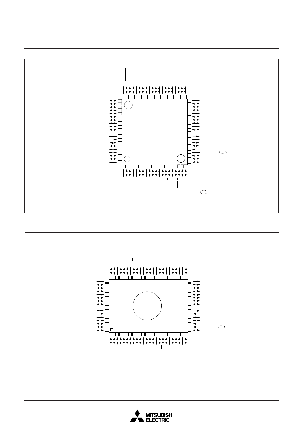
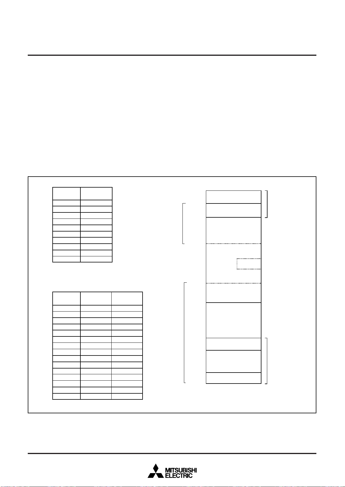
Package type : 80P6Q-A
3
1
2
1
1
1
D
D
D
/
/
/
3
4
5
1
1
1
A
A
P
P
P
1
4
4
24
4 0
P 16/ A D
3 9
3 8
3 7
3 6
3 5
3 4
3 3
3 2
3 1
3 0
2 9
2 8
2 7
2 6
2 5
2 4
2 3
2 2
2 1
0
8
9
2
1
1
1
0
D
1
S
X
/
F
T
1
/
5
4
/
R
1
P
S
/
7
C
4
S
P
/
6
4
P
O B
L K
1 4
P 17/ A D
1 5
P 20/ D B
0
P 21/ D B
1
P 22/ D B
2
P 23/ D B
3
P 24/ D B
4
P 25/ D B
5
P 26/ D B
6
P 27/ D B
7
V
S S
X
O U T
X
I N
P 40/ X
C O U
P 41/ X
C I N
R E S E
C N V
P 42/ I N T0/ O B F
P 43/ I N T1/ O B F
P 44/ R
V
S
P P
0
0 1
X
: PROM version
Note: The pin number and the position of the
function pin may change by the kind of
package.
Fig. 1 M38867M8A-XXXHP, M38867E8AHP pin configuration
PIN CONFIGURATION (TOP VIEW)
P 87/ D Q
P 86/ D Q
P 85/ D Q
P 84/ D Q
P 83/ D Q
P 82/ D Q
P 81/ D Q
P 80/ D Q
V
A
P 67/ A N
P 66/ A N
P 65/ A N
P 64/ A N
P 63/ A N
T
O
0
0
T
0
1
M
M
W
/
/
/
/
2
3
0
1
3
3
3
3
P
O N
P
R E S E
U
P W
P W
P
P
6
46
36
26
6 6
6 7
6 8
6 9
7 0
7 1
7 2
7 3
7 4
7 5
7 6
7 7
7 8
7 9
8 0
1
2
N
/
2
6
P
A
16
2345678
1
0
L
C
N
N
S
/
/
/
7
1
0
7
6
6
P
P
P
A
A
7
6
5
4
3
2
1
0
V
C C
R E F
S
S
V
7
6
5
4
3
05
A
D
S
/
6
7
P
/φ
4
3
P
I N
C
/
5
3
P
S Y N
95
1
4
T
/
5
7
P
W
85
I N
1
3
T
/
4
7
P
R
/
6
3
R
P
75
D Y
I N
1
2
T
/
2
R
S
/
3
7
P
D
/
7
3
P
P
E
A
65
L K
0
D
/
F
R
3
/
0
0
P
9
2
C
S
/
2
7
P
A
55
1
01
2
O
S
/
1
7
P
U T
1
D
/
1
0
P
11
N
2
D
/
2
0
P
A
45
2
I
S
/
0
7
P
A
35
21
D
P W
3
D
/
3
0
P
A
25
31
1
1
M
/
2
A
/
7
5
P
D
P W
4
D
/
4
0
P
1
0
M
/
1
A
/
6
5
P
A
15
41
C N T
5
D
/
5
0
P
1
R
/
5
5
P
A
04
51
C N T
6
D
/
6
0
P
0
R
/
4
5
P
A
94
61
I N
7
D
/
7
0
P
W
/
0
4
T
/
3
5
P
8
D
/
0
1
P
A
84
71
R
/
0
3
T
/
2
5
P
I N
A
74
81
I N
9
D
/
1
1
P
0
S
/
0
2
T
/
1
5
P
0
1
D
/
2
1
P
A
64
92
0
A
/
0
5
P
1
1
D
/
3
1
P
A
54
3 8 8 6 7 E 8 A F
02
1
S
/
1
R
S
/
7
4
P
D Y
A
44
S
M
12
0
1
F
/
1
C
S
/
6
4
P
L K
O B
2
1
D
/
4
1
P
A
34
22
3
1
D
/
5
1
P
D
X
T
/
5
4
P
4
1
D
/
6
1
P
A
24
32
D
X
R
/
4
4
P
5
1
D
/
7
1
P
A
1
4 06 5
P 20/ D B
3 9
3 8
3 7
3 6
3 5
3 4
3 3
3 2
3 1
3 0
2 9
2 8
2 7
2 6
2 5
4
1
0
F
/
1
T
/
3
4
P
I N
O B
0
P 21/ D B
1
P 22/ D B
2
P 23/ D B
3
P 24/ D B
4
P 25/ D B
5
P 26/ D B
6
P 27/ D B
7
V
S S
X
O U T
X
I N
P 40/ X
C O U
P 41/ X
C I N
R E S E
C N V
S S
P 42/ I N T0/ O B F
V
P P
0
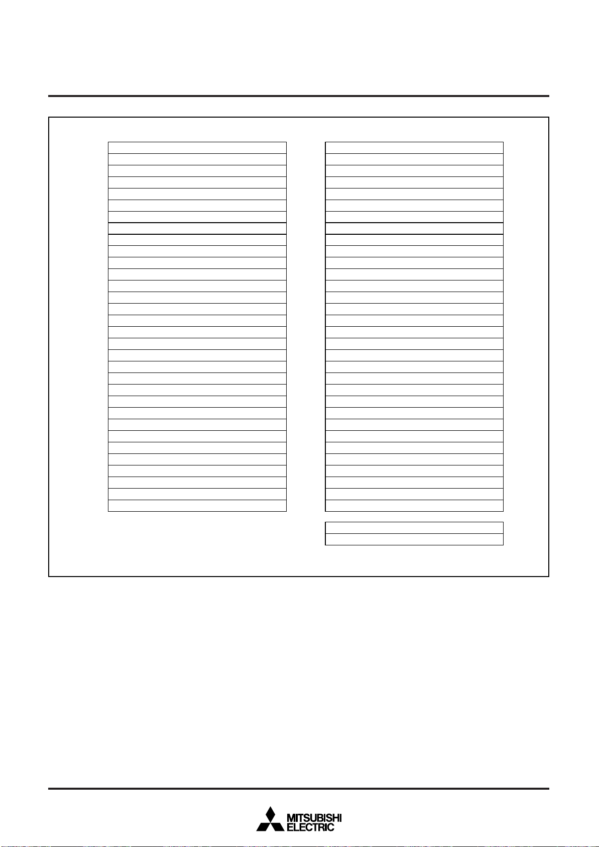
Note: The pin number and the position of
Package type : 80D0
the function pin may change by the
kind of package.
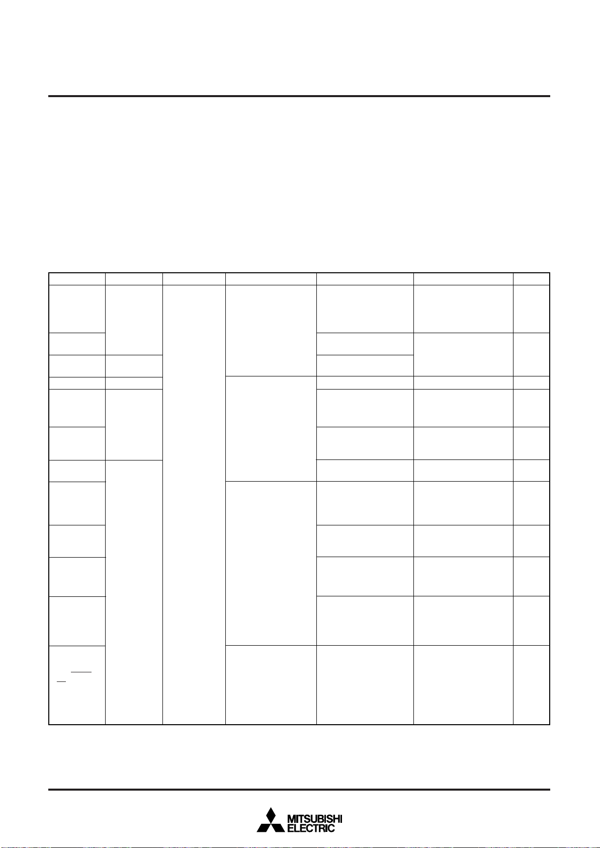
Fig. 2 M38867E8AFS pin configuration
2
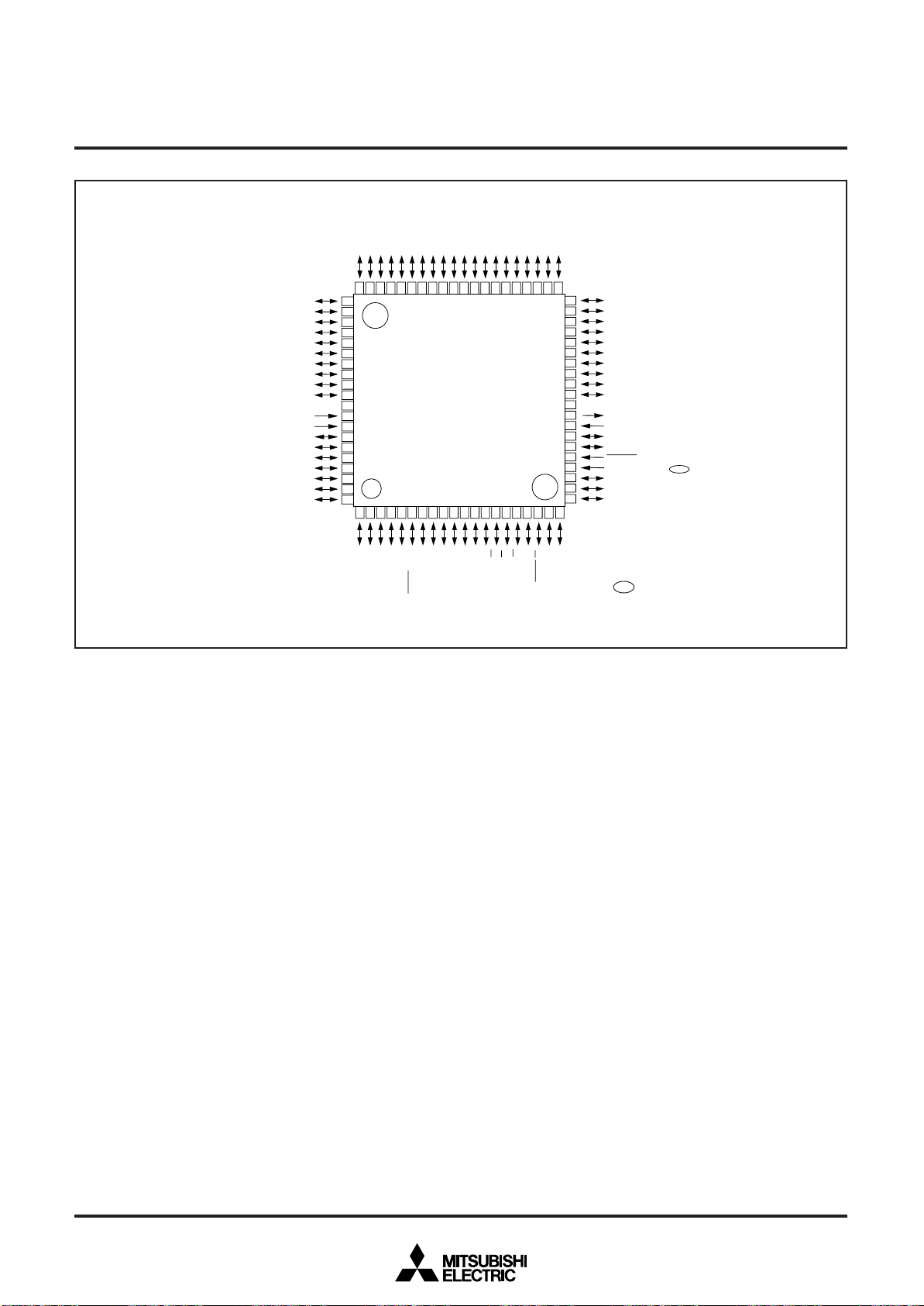
PIN CONFIGURATION (TOP VIEW)
P31/PWM10
P30/PWM00
P87/DQ7
P86/DQ6
P85/DQ5
P84/DQ4
P83/DQ3
P82/DQ2
P81/DQ1
P80/DQ0
VCC
VREF
AV
P67/AN7
P66/AN6
P65/AN5
P64/AN4
P63/AN3
P62/AN2
P61/AN1
61
62
63
64
65
66
67
68
69
70
71
72
73
SS
74
75
76
77
78
79
80
SINGLE-CHIP 8-BIT CMOS MICROCOMPUTER
REF
/P3
6
3
2
P3
P3
60
59
7
P3
P34P35P0
P3
58
57
56
55
0
2
3
P04P05P06P07P11P12P13P14P1
P01P0
P0
51
54
53
52
50
0
P1
46
44
49
48
43
47
45
M38869MFA-XXXGP/HP
M38869FFAGP/HP
2
1
3
7
9
5
4
6
8
12
11
10
17
16
15
14
13
18
MITSUBISHI MICROCOMPUTERS
3886 Group
5
41
42
40
P16
39
P17
38
P20
37
P21
36
P22
35
P23
34
P24
33
P25
32
P26
31
P27
30
VSS
29
XOUT
28
XIN
27
P40/XCOUT
26
P41/XCIN
25
RESET
24
CNVSS
23
P42/INT0/OBF00
22
P4
21
20
19
3/INT1/OBF01
P44/RXD
VPP
0
31
41
21
CL
/AN
0
P6
DA
/S
/S
7
6
/INT
/INT
4
5
P7
P7
P7
P7
/INT
RDY2
/S
3
P7
CLK2
/S
2
P7
OUT2
/S
1
P7
IN2
/S
0
P7
11
/PWM
2
/DA
7
P5
Package type : 80P6S-A/80P6Q-A
Fig. 3 M38869MFA-XXXGP/HP, M38869FFAGP/HP pin configuration
1
01
/CNTR
/PWM
5
1
P5
/DA
6
P5
0
/W
40
/CNTR
4
/INT
3
P5
P5
/R
30
/INT
2
P5
0
/S
20
/INT
1
P5
1
0
D
10
X
/S
/A
0
/T
5
P5
/OBF
RDY1
P4
/S
7
CLK1
P4
/S
6
P4
: Flash memory version
Note: The pin number and the position of the
function pin may change by the kind of
package.
3
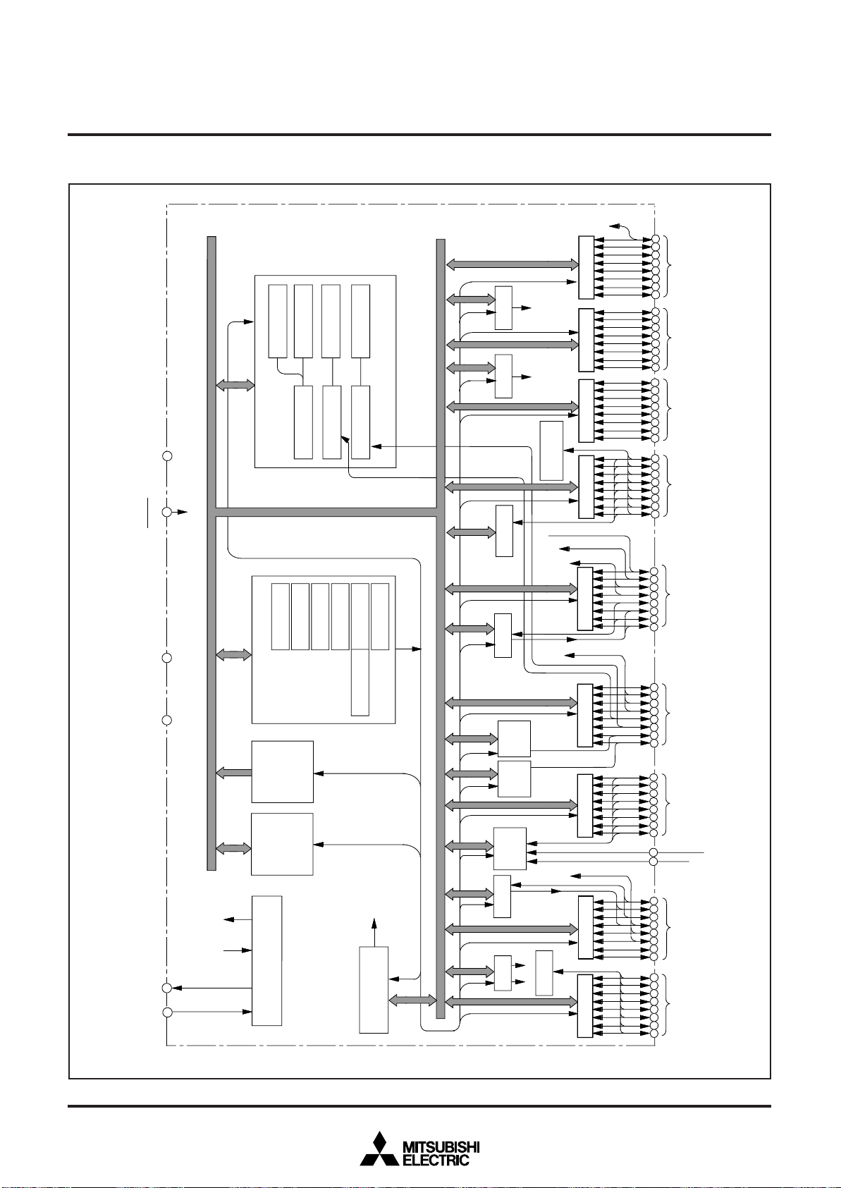
FUNCTIONAL BLOCK
I
N
T
0
,
C
N T
R
0
C
N T
R
1
V
R
E
F
A
V
S
S
R A
M
R O
M
C
P UASP
C
H
P
C
L
P
S
V
S
S
3
0
R
E S E
T
2
5
V
C
C
1
2
4
C
N
V
S
S
P
5 ( 8 )P
7 ( 8
)
24683
579
P
8 ( 8 )P
6 ( 8
)
7
47
6
8
8
0
5
7
77
917 27
3
X
I
N
2
8
9
S
I / O 1 ( 8 )S
I / O 2 ( 8
)
D
-
A
c
o n v e r t e r
2
(
8
)
R
e s e t i n p u
t
C
l o c k g e n e r a t i n g c i r c u i
t
M
a i n - c l o c ki
n p u
t
M
a i n - c l o c ko
u t p u
t
A
- D
c
o n v e r t e
r
(
1 0
)
T
i m e r Y ( 8 )T
i m e r X ( 8
)
P
r e s c a l e r 1 2 ( 8
)
P
r
e
s
c
a
l
e
r
X
(
8
)
P
r
e
s
c
a
l
e
r
Y
(
8
)
T
i m e r 1 ( 8
)
T
i m e r 2 ( 8
)
I
/ O p o r t P 5I
/ O p o r t P 7I
/ O p o r t P 8I
/ O p o r t P
6
S
u b - c l o c
k
i
n p u
t
X
O
U
T
X
C
I
N
X
C
O U
T
S
u b - c l o c
k
o
u t p u
t
W
a t c h d o
g
t
i
m
e
r
R
e s e
t
P
0 ( 8
)
P
1 ( 8 )P
2 ( 8
)
P
3 ( 8
)
I
/ O p o r t P 0I
/ O p o r t P 1I
/ O p o r t P 2I
/ O p o r t P
3
P
3
R
E
F
K
e y - o n
w
a k e - u
p
X
C
I
N
X
C
O
U
T
P
4 ( 8 )I
/ O p o r t P
4
C
o m p a r a t o
r
I
N
T
1
P
W M 0 ( 1 4 )P
W M 1 ( 1 4
)
P
W
M
0
0
,
P
W
M
0
1
P
W
M
1
0
,
P
W
M
1
1
D
Q
0
t
o
D
Q
7
B
u s i n t e r f a c
e
I
C
2
S
C
L
S
D
A
I
N
T
4
1
I
N
T
2
1
,
I
N
T
3
1
,
I
N
T
4
0
N
T
2
0
,
I
N
T
3
0
,
3
6
56
76
96
4
6
6
87
0
D
-
A
c
o n v e r t e
r
1
( 8
)
1
0
2
1
41
61
11
3
5
1
7
8
2
0
2
2
6
1
9
2
12
32
75
5
7
5
9
1
5
65
8
0
6
23
1
3
3
53
7
2
3
4
6
3
8
9
4
14
34
54
0
2
4
4
6
4
74
8
9
5
05
15
2
3
5
4
MITSUBISHI MICROCOMPUTERS
3886 Group
SINGLE-CHIP 8-BIT CMOS MICROCOMPUTER
FUNCTIONAL BLOCK DIAGRAM (Package : 80P6Q-A, 80P6S-A)
Fig. 4 Functional block diagram
4
PIN DESCRIPTION
Table 1 Pin description (1)
MITSUBISHI MICROCOMPUTERS
3886 Group
SINGLE-CHIP 8-BIT CMOS MICROCOMPUTER
VCC, VSS
CNVSS
VREF
AVSS
RESET
XIN
XOUT
P00/P3REF
P01–P07
P10–P17
P20–P27
P30/PWM
P31/PWM
P32–P37
NamePin
Power source
CNVSS input
Reference voltage
Analog power source
Reset input
Clock input
Clock output
I/O port P0
I/O port P1
I/O port P2
00
10
I/O port P3
Functions
•Apply voltage of 2.7 V – 5.5 V to Vcc, and 0 V to Vss.
•In the flash memory version, apply voltage of 4.0 V – 5.5 V to Vcc, and 0 V to Vss
•This pin controls the operation mode of the chip.
•Normally connected to VSS.
•
If this pin is connected to Vcc, the internal ROM is inhibited and an external memory is accessed.
•In the flash memory version, connected to VSS.
•In the EPROM version or the flash memory version, this pin functions as the VPP power source input pin.
•Reference voltage input pin for A-D and D-A converters.
•Analog power source input pin for A-D and D-A converters.
•Connect to VSS.
•Reset input pin for active “L”.
•Input and output pins for the clock generating circuit.
•Connect a ceramic resonator or quartz-crystal oscillator between the XIN and XOUT pins to set
the oscillation frequency.
•When an external clock is used, connect the clock source to the XIN pin and leave the XOUT
pin open.
•8-bit CMOS I/O port.
•I/O direction register allows each pin to be individually
programmed as either input or output.
•When the external memory is used, these pins are used as the address bus.
•CMOS compatible input level.
•CMOS 3-state output structure or N-channel open-drain output structure.
•8-bit CMOS I/O port.
•I/O direction register allows each pin to be individually programmed as either input or output.
•When the external memory is used, these pins are used as the address bus.
•CMOS compatible input level.
•CMOS 3-state output structure or N-channel open-drain output structure.
•8-bit CMOS I/O port.
•I/O direction register allows each pin to be individually programmed as either input or output.
•When the external memory is used, these pins are used as the data bus.
•CMOS compatible input level.
•CMOS 3-state output structure.
•P24 to P27 (4 bits) are enabled to output large current for LED drive (only in single-chip mode).
•8-bit CMOS I/O port.
•I/O direction register allows each pin to be individually
programmed as either input or output.
•When the external memory is used, these pins are
used as the control bus.
•CMOS compatible input level.
•CMOS 3-state output structure.
•These pins function as key-on wake-up and comparator input.
•These pins are enabled to control pull-up.
Function except a port function
•Comparator reference power source
input pin
•Key-on wake-up input pin
•Comparator input pin
•PWM output pin
•Key-on wake-up input pin
•Comparator input pin
5
Table 2 Pin description (2)
MITSUBISHI MICROCOMPUTERS
3886 Group
SINGLE-CHIP 8-BIT CMOS MICROCOMPUTER
P40/XCOUT
P41/XCIN
P42/INT0
/OBF00
P43/INT1
/OBF01
P44/RxD
P45/TxD
P46/SCLK1
/OBF10
P47/SRDY1
/S1
P50/A0
P51/INT20
/S0
P52/INT30
/R
P53/INT40
/W
P54/CNTR0
P55/CNTR1
P56/DA1
/PWM01
P57/DA2
/PWM11
P60/AN0–
P67/AN7
P70/SIN2
P71/SOUT2
P72/SCLK2
P73/SRDY2
/INT21
P74/INT31
P75/INT41
P76/SDA
P77/SCL
P80/DQ0–
P87/DQ7
I/O port P4
I/O port P5
I/O port P6
I/O port P7
I/O port P8
NamePin
•8-bit I/O port with the same function as port P0.
<Input level>
P40, P41 : CMOS input level
P42–P46 : CMOS compatible input level or TTL in-
put level
P47 : CMOS compatible input level or TTL input
level in the bus interface function
<Output structure>
P40, P41, P47 : CMOS 3-state output structure
P42–P46 : CMOS 3-state output structure or N-
channel open-drain output structure
•Regardless of input or output port, P42 to P46 can
be input every pin level.
•When P42 and P43 are used as output port, the
function which makes P42 and P43 clear to “0”
when the host CPU reads the output data bus
buffer 0 can be added.
•8-bit I/O port with the same function as port P0.
•CMOS compatible input level.
•CMOS 3-state output structure.
•P50 to P53 can be switched between CMOS compatible input level or TTL input level in the bus
interface function.
•8-bit I/O port with the same function as port P0.
•CMOS compatible input level.
•CMOS 3-state output structure.
•8-bit I/O port with the same function as port P0.
P70–P75 : CMOS compatible input level or TTL in-
put level
P76, P77 : CMOS compatible input level or
SMBUS input level in the I2C-BUS interface function, N-channel open-drain
output structure
•Regardless of input or output port, P70 to P75 can
be input every pin level.
•8-bit I/O port with the same function as port P0.
•CMOS compatible input level.
•CMOS 3-state output structure.
•CMOS compatible input level or TTL input level in
the bus interface function.
Functions
Function except a port function
•Sub-clock generating circuit I/O
pins
(Connect a resonator.)
•Interrupt input pins
•Bus interface function pins
•Serial I/O1 function pins
•Serial I/O1 function pins
•Bus interface function pins
•Bus interface function pins
•Interrupt input pins
•Bus interface function pins
•Timer X, timer Y function pins
•D-A converter output pin
•PWM output pin
•A-D converter output pin
•Serial I/O2 function pin
•Serial I/O2 function pin
•Interrupt input pin
•Interrupt input pin
•I2C-BUS interface function pin
•Bus interface function pin
6
PART NUMBERING
MITSUBISHI MICROCOMPUTERS
3886 Group
SINGLE-CHIP 8-BIT CMOS MICROCOMPUTER
P r o d u c t n a m e
M 3 8 8 6 7 M 8 A - X X X H P
P a c k a g e t y p e
H P : 8 0 P 6 Q - A
G P : 8 0 P 6 S - A
F S : 8 0 D 0
R O M n u m b e r
O m i t t e d i n t h e o n e t i m e P R O M v e r s i o n s h i p p e d i n b l a n k ,
t h e E P R O M v e r s i o n a n d t h e f l a s h m e m o r y v e r s i o n .
A – : H i g h - s p e e d v e r s i o n
– i s o m i t t e d i n t h e O n e T i m e P R O M v e r s i o n s h i p p e d i n b l a n k ,
t h e E P R O M v e r s i o n a n d t h e f l a s h m e m o r y v e r s i o n .
R O M / P R O M s i z e
1
: 4 0 9 6 b y t e s
2
: 8 1 9 2 b y t e s
3
: 1 2 2 8 8 b y t e s
4
: 1 6 3 8 4 b y t e s
5
: 2 0 4 8 0 b y t e s
6
: 2 4 5 7 6 b y t e s
7
: 2 8 6 7 2 b y t e s
8
: 3 2 7 6 8 b y t e s
T h e f i r s t 1 2 8 b y t e s a n d t h e l a s t 2 b y t e s o f R O M a r e r e s e r v e d
a r e a s ; t h e y c a n n o t b e u s e d .
H o w e v e r , t h e y c a n b e p r o g r a m m e d o r e r a s e d i n t h e E P R O M
v e r s i o n a n d t h e f l a s h m e m o r y v e r s i o n , s o t h a t t h e u s e r s c a n
u s e t h e m .
9
: 3 6 8 6 4 b y t e s
A
: 4 0 9 6 0 b y t e s
B
: 4 5 0 5 6 b y t e s
C
: 4 9 1 5 2 b y t e s
D
: 5 3 2 4 8 b y t e s
E
: 5 7 3 4 4 b y t e s
F
: 6 1 4 4 0 b y t e s
Fig. 5 Part numbering
M e m o r y t y p e
M
: M a s k R O M v e r s i o n
E
: E P R O M o r O n e T i m e P R O M v e r s i o n
F
: F l a s h m e m o r y v e r s i o n
R A M s i z e
0
: 1 9 2 b y t e s
1
: 2 5 6 b y t e s
2
: 3 8 4 b y t e s
3
: 5 1 2 b y t e s
4
: 6 4 0 b y t e s
5
: 7 6 8 b y t e s
6
: 8 9 6 b y t e s
7
: 1 0 2 4 b y t e s
8
: 1 5 3 6 b y t e s
9
: 2 0 4 8 b y t e s
7
MITSUBISHI MICROCOMPUTERS
/
K
O
)
K
K
K
K
K
K
K
8
6
0
6
K
O
(
)
/
C
3886 Group
SINGLE-CHIP 8-BIT CMOS MICROCOMPUTER
GROUP EXPANSION
Mitsubishi plans to expand the 3886 group as follows.
Memory Type
Support for mask ROM, One Time PROM, EPROM and flash
memory version.
Memory Size
ROM size ........................................................... 32 K to 60 K bytes
RAM size ..........................................................1024 to 2048 bytes
Memory Expansion
M s i z e ( b y t e s
R
R
e x t e r n a l
6 0
4 8
3 2
2 8
2 4
2 0
1 6
1 2
M
8
: M a s s p r o d u c t i o n
M 8
M 3 8 8 6 7 E 8 A
Packages
80P6Q-A .................................. 0.5 mm-pitch plastic molded LQFP
80P6S-A ...................................0.65mm pitch plastic molded QFP
80D0 ....................... 0.8 mm-pitch ceramic LCC (EPROM version)
The pin number and the position of the function pin may change
by the kind of package.
M F
M 3 8 8 6 9 F F A
M 3 8 8 6 9 M
A
A
A
M 3 8 8 6 9 M 8 A
Fig. 6 Memory expansion plan
Currently products are listed below.
Table 3 Support products
Product name
(P) ROM size (bytes)
ROM size for User in ( )
M38867M8A-XXXHP
M38867E8A-XXXHP
M38867E8AHP
M38867E8AFS
32768 (32638)
M38869M8A-XXXHP
M38869M8A-XXXGP
M38869MCA-XXXHP
M38869MCA-XXXGP
49152 (19022)
M38869MFA-XXXHP
M38869MFA-XXXGP
M38869FFAHP
61440 (61310)
M38869FFAGP
3 8 45 1 26 4 01
RAM size (bytes)
7 6 88 9
1 0 2 41 1 5 21 2 8
b y t e s
R A M s i z e
Package
4 0
1 5 3
2 0 4 83 0 7 24 0 3 2
Remarks
Mask ROM version
1024
80P6Q-A
One Time PROM version
One Time PROM version (blank)
80D0
EPROM version
80P6Q-A
80P6S-A
80P6Q-A
2048
80P6S-A
Mask ROM version
80P6Q-A
80P6S-A
80P6Q-A
80P6S-A
Flash memory version
As of Jan. 2000
8
FUNCTIONAL DESCRIPTION
CENTRAL PROCESSING UNIT (CPU)
The 3886 group uses the standard 740 Family instruction set. Refer to the table of 740 Family addressing modes and machine
instructions or the 740 Family Software Manual for details on the
instruction set.
Machine-resident 740 Family instructions are as follows:
The FST and SLW instructions cannot be used.
The STP, WIT, MUL, and DIV instructions can be used.
[CPU Mode Register (CPUM)] 003B16
The CPU mode register contains the stack page selection bit, the
processor mode bits specifying the chip operation mode, etc.
The CPU mode register is allocated at address 003B16.
MITSUBISHI MICROCOMPUTERS
3886 Group
SINGLE-CHIP 8-BIT CMOS MICROCOMPUTER
b 7
N o t e : T h i s m o d e i s n o t a v a i l a b l e f o r M 3 8 8 6 9 M 8 A / M C A / M F A a n d t h e f l a s h m e m o r y v e r s i o n .
b 0
C P U m o d e r e g i s t e r
P U M : a d d r e s s
0 3
(C
0
P r o c e s s o r m o d e b i t s
b 1 b 0
0 0 : S i n g l e - c h i p m o d e
0 1 : M e m o r y e x p a n s i o n m o d e (N o t e)
1 0 : M i c r o p r o c e s s o r m o d e (N o t e)
1 1 : N o t a v a i l a b l e
S t a c k p a g e s e l e c t i o n b i t
0 : 0 p a g e
1 : 1 p a g e
I
O U
o s c i l l a t i o n f u n c t i o n .
R e s e r v e d
( D o n o t w r i t e “ 0 ” t o t h i s b i t w h e n u s i n g
XC
N–
XC
T
I
O U
o s c i l l a t i n g f u n c t i o
P o r t XC s w i t c h b i t
0 : I / O p o r t f u n c t i o n ( s t o p o s c i l l a t i n g )
1 : XC
N–
XC
U
s t o p b i t
M a i n c l o c k ( XI
N–
0 : O s c i l l a t i n g
1 : S t o p p e d
/ 2 ( h i g h - s p e e d m o d e
/ 8 ( m i d d l e - s p e e d m o d e
I
/ 2 ( l o w - s p e e d m o d e
M a i n c l o c k d i v i s i o n r a t i o s e l e c t i o n b i t s
b 7 b 6
0 0 : φ = f ( XI
0 1 : φ = f ( XI
1 0 : φ = f ( XC
1 1 : N o t a v a i l a b l e
B1
T
XO
N)
N)
N)
Fig. 7 Structure of CPU mode register
6)
)
n
T)
)
)
)
9
MITSUBISHI MICROCOMPUTERS
a
)
3886 Group
SINGLE-CHIP 8-BIT CMOS MICROCOMPUTER
MEMORY
Special Function Register (SFR) Area
The Special Function Register area in the zero page contains control registers such as I/O ports and timers.
RAM
RAM is used for data storage and for stack area of subroutine
calls and interrupts.
ROM
The first 128 bytes and the last 2 bytes of ROM are reserved for
device testing and the rest is user area for storing programs. Program/Erase of the reserved ROM area is possible in the EPROM
version and the flash memory version
R A M a r e a
R A M s i z e
( b y t e s )
1 9 2
2 5 6
3 8 4
5 1 2
6 4 0
7 6 8
8 9 6
1 0 2 4
1 5 3 6
2 0 4 8
A d d r e s s
X X X X
0 0 F F
0 1 3 F
0 1 B F
0 2 3 F
0 2 B F
0 3 3 F
0 3 B F
0 4 3 F
0 6 3 F
0 8 3 F
1 6
1 6
1 6
1 6
1 6
1 6
1 6
1 6
1 6
1 6
1 6
Interrupt Vector Area
The interrupt vector area contains reset and interrupt vectors.
Zero Page
Access to this area with only 2 bytes is possible in the zero page
addressing mode.
Special Page
Access to this area with only 2 bytes is possible in the special
page addressing mode.
0 0 0 0
R A M
0 0 4 0
0 1 0 0
X X X X
0 F F E
0 F F F
1 6
1 6
1 6
1 6
1 6
1 6
S F R a r e a
N o t u s e d
S F R a r e a
Z e r o p a g e
( N o t e 1
R O M a r e a
R O M s i z e
( b y t e s )
4 0 9 6
8 1 9 2
1 2 2 8 8
1 6 3 8 4
2 0 4 8 0
2 4 5 7 6
2 8 6 7 2
3 2 7 6 8
3 6 8 6 4
4 0 9 6 0
4 5 0 5 6
4 9 1 5 2
5 3 2 4 8
5 7 3 4 4
6 1 4 4 0
Fig. 8 Memory map diagram
A d d r e s s
Y Y Y Y
F 0 0 0
E 0 0 0
D 0 0 0
C 0 0 0
B 0 0 0
A 0 0 0
9 0 0 0
8 0 0 0
7 0 0 0
6 0 0 0
5 0 0 0
4 0 0 0
3 0 0 0
2 0 0 0
1 0 0 0
Y Y Y Y
1 6
R e s e r v e d R O M a r e a
A d d r e s s
1 6
1 6
1 6
1 6
1 6
1 6
1 6
1 6
1 6
1 6
1 6
1 6
1 6
1 6
1 6
1 6
Z Z Z Z
F 0 8 0
E 0 8 0
D 0 8 0
C 0 8 0
B 0 8 0
A 0 8 0
9 0 8 0
8 0 8 0
7 0 8 0
6 0 8 0
5 0 8 0
4 0 8 0
3 0 8 0
2 0 8 0
1 0 8 0
1 6
1 6
1 6
1 6
1 6
1 6
1 6
1 6
1 6
1 6
1 6
1 6
1 6
1 6
1 6
1 6
N o t e s 1 :
Z Z Z Z
R O M
F F 0 0
F F D C
F F F E
F F F F
T h i s a r e a i s S F R i n M 3 8 8 6 9 F F A .
T h i s a r e a i s R e s e r v e d i n M 3 8 8 6 9 M F A / M C A / M 8 A .
T h i s a r e a i s n o t u s e d i n M 3 8 8 6 7 M 8 A / E 8 A .
2 : T h i s a r e a i s u sa b l e i n E P R O M v e r s i o n a n d f l a s h m e m o r y v e r s i o n .
( N o t e 2 )
1 6
1 6
1 6
I n t e r r u p t v e c t o r a r e a
1 6
R e s e r v e d R O M a r e
1 6
( N o t e 2 )
( 1 2 8 b y t e s )
S p e c i a l p a g e
10
MITSUBISHI MICROCOMPUTERS
3886 Group
SINGLE-CHIP 8-BIT CMOS MICROCOMPUTER
P o r t P 0 ( P 0 )
0 0 0 0
1 6
P o r t P 0 d i r e c t i o n r e g i s t e r ( P 0 D )
0 0 0 1
1 6
P o r t P 1 ( P 1 )
0 0 0 2
1 6
P o r t P 1 d i r e c t i o n r e g i s t e r ( P 1 D )
0 0 0 3
1 6
P o r t P 2 ( P 2 )
0 0 0 4
1 6
P o r t P 2 d i r e c t i o n r e g i s t e r ( P 2 D )
0 0 0 5
1 6
P o r t P 3 ( P 3 )
0 0 0 6
1 6
P o r t P 3 d i r e c t i o n r e g i s t e r ( P 3 D )
0 0 0 7
1 6
P o r t P 4 ( P 4 )
0 0 0 8
1 6
P o r t P 4 d i r e c t i o n r e g i s t e r ( P 4 D )
0 0 0 9
1 6
P o r t P 5 ( P 5 )
0 0 0 A
1 6
P o r t P 5 d i r e c t i o n r e g i s t e r ( P 5 D )
0 0 0 B
1 6
P o r t P 6 ( P 6 )
0 0 0 C
1 6
P o r t P 6 d i r e c t i o n r e g i s t e r ( P 6 D )
0 0 0 D
1 6
P o r t P 7 ( P 7 )
0 0 0 E
1 6
P o r t P 7 d i r e c t i o n r e g i s t e r ( P 7 D )
0 0 0 F
1 6
P o r t P 8 ( P 8 ) / P o r t P 4 i n p u t r e g i s t e r ( P 4 I )
0 0 1 0
1 6
0 0 1 1
1 6
P o r t P 8 d i r e c t i o n r e g i s t e r ( P 8 D ) / P o r t P 7 i n p u t r e g i s t e r ( P 7 I )
0 0 1 2
0 0 1 3
0 0 1 4
0 0 1 5
0 0 1 6
0 0 1 7
0 0 1 8
0 0 1 9
0 0 1 A
0 0 1 B
0 0 1 C
0 0 1 D
0 0 1 E
0 0 1 F
2
1 6
I
C d a t a s h i f t r e g i s t e r ( S 0 )
2
1 6
I
C a d d r e s s r e g i s t e r ( S 0 D )
2
1 6
I
C s t a t u s r e g i s t e r ( S 1 )
2
1 6
I
C c o n t r o l r e g i s t e r ( S 1 D )
2
1 6
I
C c l o c k c o n t r o l r e g i s t e r ( S 2 )
2
1 6
I
C s t a r t / s t o p c o n d i t i o n c o n t r o l r e g i s t e r ( S 2 D )
T r a n s m i t / R e c e i v e b u f f e r r e g i s t e r ( T B / R B )
1 6
S e r i a l I / O 1 s t a t u s r e g i s t e r ( S I O 1 S T S )
1 6
S e r i a l I / O 1 c o n t r o l r e g i s t e r ( S I O 1 C O N )
1 6
U A R T c o n t r o l r e g i s t e r ( U A R T C O N )
1 6
B a u d r a t e g e n e r a t o r ( B R G )
1 6
S e r i a l I / O 2 c o n t r o l r e g i s t e r ( S I O 2 C O N )
1 6
W a t c h d o g t i m e r c o n t r o l r e g i s t e r ( W D T C O N )
1 6
S e r i a l I / O 2 r e g i s t e r ( S I O 2 )
1 6
P r e s c a l e r 1 2 ( P R E 1 2 )
0 0 2 0
1 6
T i m e r 1 ( T 1 )
0 0 2 1
1 6
T i m e r 2 ( T 2 )
0 0 2 2
1 6
T i m e r X Y m o d e r e g i s t e r ( T M )
0 0 2 3
1 6
P r e s c a l e r X ( P R E X )
0 0 2 4
1 6
T i m e r X ( T X )
0 0 2 5
1 6
P r e s c a l e r Y ( P R E Y )
0 0 2 6
1 6
T i m e r Y ( T Y )
0 0 2 7
1 6
0 0 2 8
1 6
D a t a b a s b u f f e r r e g i s t e r 0 ( D B B 0 )
0 0 2 9
1 6
D a t a b a s b u f f e r s t a t u s r e g i s t e r 0 ( D B B S T S 0 )
D a t a b a s b u f f e r c o n t r o l r e g i s t e r ( D B B C O N )
0 0 2 A
1 6
D a t a b a s b u f f e r r e g i s t e r 1 ( D B B 1 )
0 0 2 B
1 6
D a t a b a s b u f f e r s t a t u s r e g i s t e r 1 ( D B B S T S 1 )
0 0 2 C
1 6
C o m p a r a t o r d a t a r e g i s t e r ( C M P D )
0 0 2 D
1 6
P o r t c o n t r o l r e g i s t e r 1 ( P C T L 1 )
0 0 2 E
1 6
P o r t c o n t r o l r e g i s t e r 2 ( P C T L 2 )
0 0 2 F
1 6
P W M 0 H r e g i s t e r ( P W M 0 H )
0 0 3 0
1 6
P W M 0 L r e g i s t e r ( P W M 0 L )
0 0 3 1
1 6
P W M 1 H r e g i s t e r ( P W M 1 H )
0 0 3 2
1 6
P W M 1 L r e g i s t e r ( P W M 1 L )
0 0 3 3
1 6
A D / D A c o n t r o l r e g i s t e r ( A D C O N )
0 0 3 4
1 6
A - D c o n v e r s i o n r e g i s t e r 1 ( A D 1 )
0 0 3 5
1 6
D - A 1 c o n v e r s i o n r e g i s t e r ( D A 1 )
0 0 3 6
1 6
D - A 2 c o n v e r s i o n r e g i s t e r ( D A 2 )
0 0 3 7
1 6
A - D c o n v e r s i o n r e g i s t e r 2 ( A D 2 )
0 0 3 8
1 6
I n t e r r u p t s o u r c e s e l e c t i o n r e g i s t e r ( I N T S E L )
0 0 3 9
1 6
I n t e r r u p t e d g e s e l e c t i o n r e g i s t e r ( I N T E D G E )
0 0 3 A
1 6
C P U m o d e r e g i s t e r ( C P U M )
0 0 3 B
1 6
I n t e r r u p t r e q u e s t r e g i s t e r 1 ( I R E Q 1 )
0 0 3 C
1 6
I n t e r r u p t r e q u e s t r e g i s t e r 2 ( I R E Q 2 )
0 0 3 D
1 6
I n t e r r u p t c o n t r o l r e g i s t e r 1 ( I C O N 1 )
0 0 3 E
1 6
I n t e r r u p t c o n t r o l r e g i s t e r 2 ( I C O N 2 )
0 0 3 F
1 6
Fig. 9 Memory map of special function register (SFR)
F l a s h m e m o r y c o n t r o l r e g i s t e r ( F C O N )
0 F F E
1 6
F l a s h c o m m a n d r e g i s t e r ( F C M D )
0 F F F
1 6
N o t e : F l a s h m e m o r y v e r s i o n o n l y
( N o t e )
( N o t e )
11
MITSUBISHI MICROCOMPUTERS
3886 Group
SINGLE-CHIP 8-BIT CMOS MICROCOMPUTER
I/O PORTS
The I/O ports have direction registers which determine the input/
output direction of each individual pin. Each bit in a direction register corresponds to one pin, and each pin can be set to be input
port or output port.
When “0” is written to the bit corresponding to a pin, that pin becomes an input pin. When “1” is written to that bit, that pin
becomes an output pin.
If data is read from a pin which is set to output, the value of the
port output latch is read, not the value of the pin itself. Pins set to
input are floating. If a pin set to input is written to, only the port
Table 4 I/O port function (1)
Pin
P00/P3REF
P01–P07
P10–P17
P20–P27
P30/PWM00
P31/PWM10
P32–P37
P40/XCOUT
P41/XCIN
P42/INT0/
OBF00
P43/INT1/
OBF01
P44/RXD
P45/TXD
P46/SCLK1
/OBF10
P47/SRDY1
/S1
Name
Port P0
Port P1
Port P2
Port P3
Port P4
Input/Output
Input/output,
individual bits
I/O Structure Non-Port Function
CMOS compatible
input level
CMOS 3-state output
or N-channel opendrain output
CMOS compatible
input level
CMOS 3-state output
CMOS compatible
input level or TTL
input level
CMOS 3-state output
or N-channel opendrain output
CMOS compatible
input level
CMOS 3-state output
(when selecting bus
interface function)
CMOS compatible
input level or TTL
input level
output latch is written to and the pin remains floating.
When the P8 function select bit of the port control register 2 (address 002F16) is set to “1”, read from address 001016 becomes
the port P4 input register, and read from address 001116 becomes
the port P7 input register.
As the particular function, value of P42 to P46 pins and P70 to P75
pins can be read regardless of setting direction registers, by reading the port P4 input register (address 001016) or the port P7 input
register (address 001116) respectively.
Ref.No.
(1)
(2)
(3)
(4)
(5)
(6)
(7)
(8)
(9)
(10)
(11)
(12)
(13)
(14)
Address low-order byte
output
Analog comparator
power source input pin
Address low-order byte
output
Address high-order
byte output
Data bus I/O
Control signal I/O
PWM output
Key-on wake up input
Comparator input
Control signal I/O
Key-on wake up input
Comparator input
Sub-clock generating
circuit
External interrupt input
Bus interface function
I/O
Serial I/O1 function input
Serial I/O1 function output
Serial I/O1 function I/O
Bus interface function
output
Serial I/O1 function output
Bus interface function
input
Related SFRs
CPU mode register
Port control register 1
Serial I/O2 control
register
CPU mode register
Port control register 1
CPU mode register
CPU mode register
Port control register 1
AD/DA control register
CPU mode register
Port control register 1
CPU mode register
Interrupt edge selection
register
Port control register 2
Serial I/O1 control
register
Port control register 2
Serial I/O1 control
register
UART control register
Port control register 2
Serial I/O1 control
register
Data bus buffer control
register
Port control register 2
Serial I/O1 control
register
Data bus buffer control
register
12
MITSUBISHI MICROCOMPUTERS
3886 Group
SINGLE-CHIP 8-BIT CMOS MICROCOMPUTER
Table 5 I/O port function (2)
Pin
P50/A0
P51/INT20
/S0
P52/INT30
/R
P53/INT40
/W
P54/CNTR0
P55/CNTR1
P56/DA1/
PWM01
P57/DA2/
PWM11
P60/AN0–
P67/AN7
P70/SIN2
P71/SOUT2
P72/SCLK2
P73/SRDY2/
INT21
P74/INT31
P75/INT41
P76/SDA
P77/SCL
P80/DQ0–
P87/DQ7
Notes1: For details of the functions of ports P0 to P3 in modes other than single-chip mode, and how to use double-function ports as function I/O ports, refer
to the applicable sections.
2: Make sure that the input level at each pin is either 0 V or V
When an input level is at an intermediate potential, a current will flow from V
Name
Port P5
Port P6
Port P7
Port P8
Input/Output I/O Format
CMOS compatible
input level
CMOS 3-state output
(when selecting bus
interface function)
CMOS compatible
input level or TTL
input level
CMOS compatible
input level
CMOS 3-state output
Input/output,
individual bits
CMOS compatible
input level or TTL
input level
N-channel open-drain
output
CMOS compatible
input level
N-channel open-drain
output
(when selecting I2CBUS interface
function)
CMOS compatible
input level or SMBUS
input level
CMOS compatible
input level
CMOS 3-state output
(when selecting bus
interface function)
CMOS compatible
input level or TTL
input level
CC during execution of the STP instruction.
Non-Port Function
Bus interface function
input
External interrupt input
Bus interface function
input
Timer X, timer Y function I/O
D-A converter output
PWM output
A-D converter input
Serial I/O2 function I/O
Serial I/O2 function output
Bus interface function
input
External interrupt input
I2C-BUS interface function I/O
Bus interface function
I/O
CC to VSS through the input-stage gate.
Related SFRs
Data bus buffer control
register
Interrupt edge selection
register
Data bus buffer control
register
Timer XY mode register
AD/DA control register
UART control register
AD/DA control register
Serial I/O2 control
register
Port control register 2
Serial I/O2 control
register
Port control register 2
Interrupt edge selection
register
Port control register 2
I2C control register
Data bus buffer control
register
Ref.No.
(15)
(16)
(17)
(18)
(19)
(20)
(21)
(22)
(23)
(24)
(25)
(26)
(27)
(28)
13
MITSUBISHI MICROCOMPUTERS
e
s
t
t
t
3886 Group
SINGLE-CHIP 8-BIT CMOS MICROCOMPUTER
( 1 ) P o r t P 0
D a t a b u s P o r t l a t c h
P
0
P 0
0–
s t r u c t u r e s e l e c t i o n b i t
C o m p a r a t o r r e f e r e n c e p o w e r s o u r c e i n p u t
03 o u t p u t
D i r e c t i o n
r e g i s t e r
( 3 ) P o r t P 2
D i r e c t i o n
r e g i s t e r
D a t a b u s
P o r t l a t c h
C o m p a r a t o r r e f e r e n c e i n p u t
p i n s e l e c t b i t
( 2 ) P o r t s P 01– P 07, P 1
( 4 ) P o r t P 3
P
P
P
P 00– P 03,
4–
07,
P 0
P 1
0–
13,
o u t p u t s t r u c t u r
P 1
4–
17
s e l e c t i o n b i t
D i r e c t i o n
r e g i s t e r
D a t a b u s
P W M0 o u t p u t p i n s e l e c t i o n b i t
D a t a b u s
0
e n a b l e b i
P W M
o u t p u
P W M
P o r t l a t c h
0
D i r e c t i o n
r e g i s t e r
P o r t l a t c h
0 0
P
P 3
0–
t
33 p u l l - u p c o n t r o l b i t
C o m p a r a t o r
K e y - o n w a k e - u p
i n p u t
( 5 ) P o r t P 3
P W M1 o u t p u t p i n s e l e c t i o n b i t
D a t a b u s
( 7 ) P o r t P 4
D a t a b u s
1
e n a b l e b i
1
P W M
D i r e c t i o n
r e g i s t e r
P o r t l a t c h
o u t p u
1 0
P W M
0
P o r t XC s w i t c h b i t
D i r e c t i o n
r e g i s t e r
P o r t l a t c h
P 30– P 33 p u l l - u p c o n t r o l b i t
t
P o r t P 4
C o m p a r a t o r
K e y - o n w a k e - u p
O s c i l l a t o r
1
( 6 ) P o r t s P 32– P 3
D a t a b u sP
i n p u t
( 8 ) P o r t P 4
s w i t c h b i
P o r t X
D a t a b u s
7
P
P 30– P 33,
p u l l - u p c o n t r o l b i t
P 3
4–
37
D i r e c t i o n
r e g i s t e r
o r t l a t c
h
1
C
t
D i r e c t i o n
r e g i s t e r
P o r t l a t c h
S u b - c l o c k g e n e r a t i n g c i r c u i t i n p u
C o m p a r a t o r
K e y - o n w a k e - u p
i n p u t
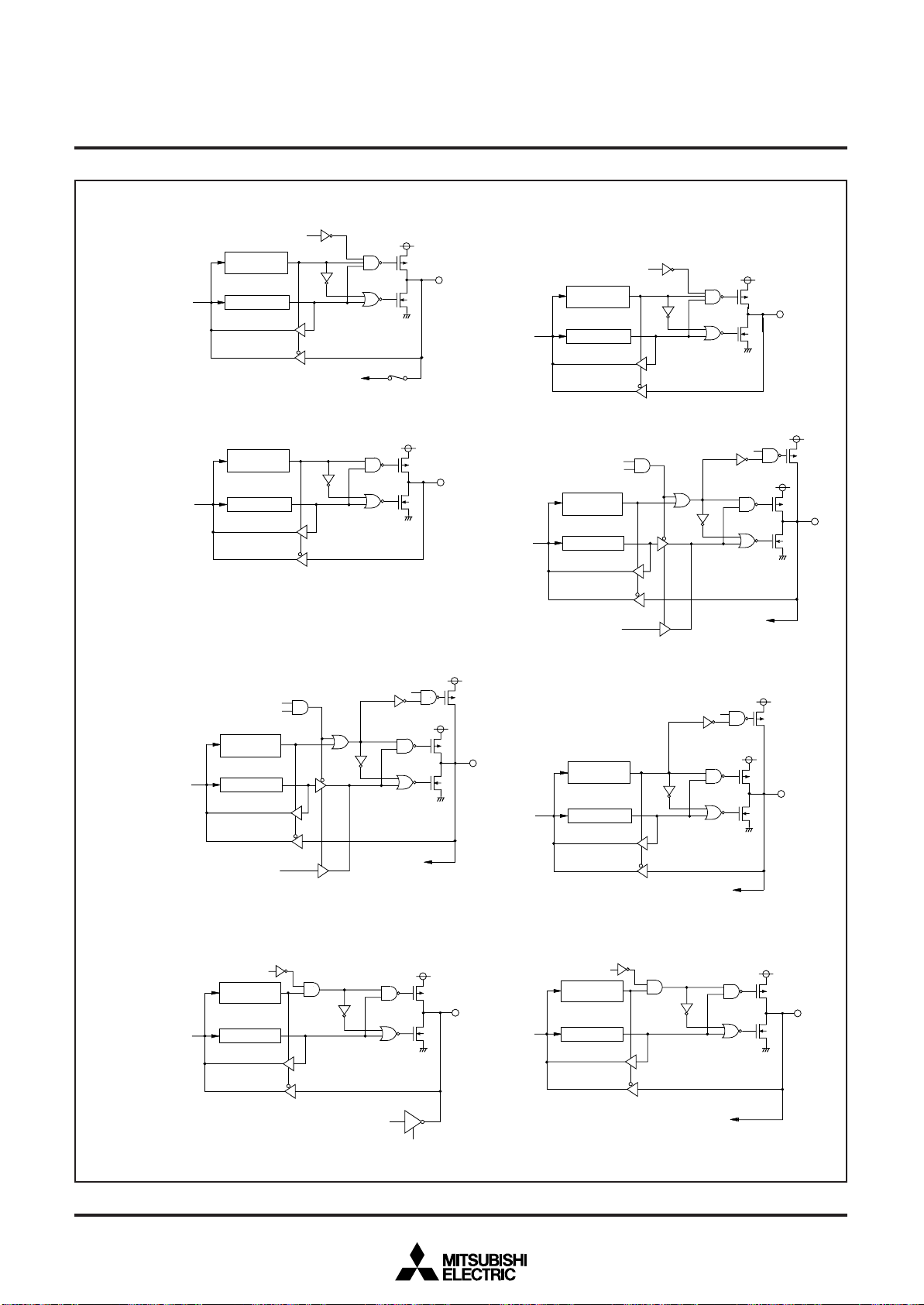
Fig. 10 Port block diagram (1)
14
P o r t XC s w i t c h b i t
MITSUBISHI MICROCOMPUTERS
s
t
t
t
s
t
t
s
t
t
t
t
t
s
t
s
t
t
s
t
t
t
s
s
3886 Group
SINGLE-CHIP 8-BIT CMOS MICROCOMPUTER
( 9 ) P o r t P 4
( 1 1 ) P o r t P 4
( 1 3 ) P o r t P 4
S e r i a l I / O 1
s y n c h r o n o u s c l o c k s e l e c t i o n b i t
2
P 4 o u t p u t s t r u c t u r e s e l e c t i o n b i
0 0
o u t p u t e n a b l e b i
O B F
D i r e c t i o n
r e g i s t e r
D a t a b u
S e r i a l I / O 1 e n a b l e b i
D a t a b u
S e r i a l I / O 1 e n a b l e b i t
S e r i a l I / O 1 m o d e s e l e c t i o n b i
D a t a b u
P o r t l a t c h
O B F
4
P 4 o u t p u t s t r u c t u r e s e l e c t i o n b i
R e c e i v e e n a b l e b i
D i r e c t i o n
r e g i s t e r
P o r t l a t c h
6
S e r i a l I / O 1 e n a b l e b i
O B F
1 0
o u t p u t e n a b l e b i t
D i r e c t i o n
r e g i s t e r
P o r t l a t c h
✻1
✻2
0 0
o u t p u t
I N T0 i n t e r r u p t i n p u t
✻1
✻2
S e r i a l I / O 1 i n p u t
P 4 o u t p u t s t r u c t u r e s e l e c t i o n b i
( 1 0 ) P o r t P 4
D a t a b u
( 1 2 ) P o r t P 4
P 4
5
/ TXD P - c h a n n e l o u t p u t d i s a b l e b i t
S e r i a l I / O 1 e n a b l e b i
T r a n s m i t e n a b l e b i
D a t a b u
S e r i a l I / O 1 o u t p u t
( 1 4 ) P o r t P 4
S e r i a l I / O 1 m o d e s e l e c t i o n b i
D a t a b u s b u f f e r f u n c t i o n
D a t a b u
3
P 4 o u t p u t s t r u c t u r e s e l e c t i o n b i
0 1
o u t p u t e n a b l e b i t
O B F
D i r e c t i o n
r e g i s t e r
P o r t l a t c h
✻1
✻2
0 1
o u t p u t
O B F
5
D i r e c t i o n
r e g i s t e r
P o r t l a t c h
7
S e r i a l I / O 1 e n a b l e b i t
R D Y 1
o u t p u t e n a b l e b i
S
s e l e c t i o n b i t
D i r e c t i o n
r e g i s t e r
P o r t l a t c h
I N T1 i n t e r r u p t i n p u t
✻1
✻2
S e r i a l I / O 1 c l o c k o u t p u t
O B F
( 1 5 ) P o r t P 5
D a t a b u s b u f f e r e n a b l e b i
D a t a b u
✻1 .T h e i n p u t l e v e l c a n b e s w i t c h e d b e t w e e n C M O S c o m p a t i b l e i n p u t l e v e l a n d T T L l e v e l b y t h e P 4 i n p u t l e v e l s e l e c t i o n b i t o f t h e p o r t c o n t r o l
✻2 .T h e i n p u t l e v e l c a n b e s w i t c h e d b e t w e e n C M O S c o m p a t i b l e i n p u t l e v e l a n d T T L l e v e l b y t h e P 4 i n p u t l e v e l s e l e c t i o n b i t o f t h e p o r t c o n t r o l
✻3 .T h e i n p u t l e v e l c a n b e s w i t c h e d b e t w e e n C M O S c o m p a t i b l e i n p u t l e v e l a n d T T L l e v e l b y t h e i n p u t l e v e l s e l e c t i o n b i t o f t h e d a t a b u s b u f f e r
0
D i r e c t i o n
r e g i s t e r
P o r t l a t c h
r e g i s t e r 2 ( a d d r e s s 0 0 2 F
r e g i s t e r 2 ( a d d r e s s 0 0 2 F
T h e p o r t P 8 a n d p o r t P 4 i n p u t r e g i s t e r c a n b e s w i t c h e d b y t h e P 8 f u n c t i o n s e l e c t i o n b i t o f t h e p o r t c o n t r o l r e g i s t e r 2 ( a d d r e s s 0 0 2 F
c o n t r o l r e g i s t e r ( a d d r e s s 0 0 2 A
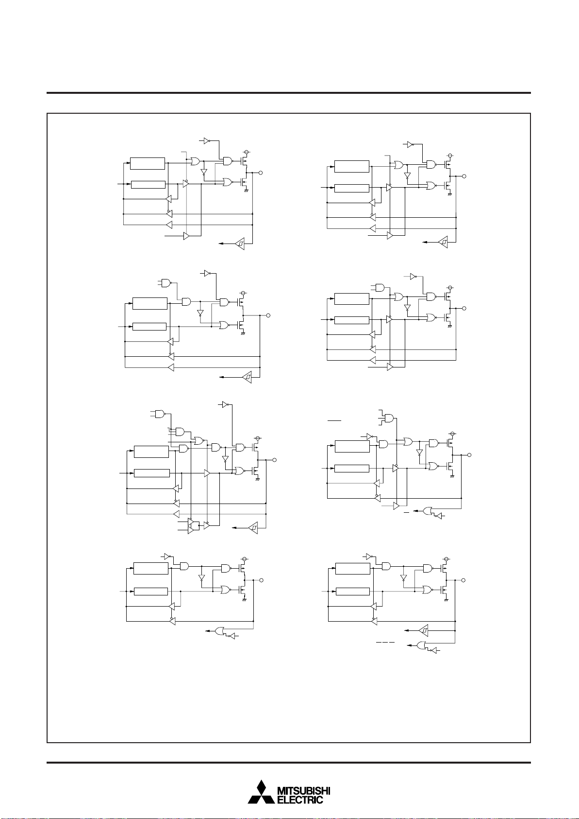
Fig. 11 Port block diagram (2)
1 0
o u t p u t
✻1
✻2
S e r i a l I / O 1 e x t e r n a l c l o c k i n p u t
( 1 6 ) P o r t s P 51, P 52, P 5
A
0
i n p u
1 6
) .
1 6
) .
1 6
) .
✻3
D a t a b u s b u f f e r
e n a b l e b i t
S e r i a l I / O 1 r e a d y o u t p u t
D a t a b u s b u f f e r e n a b l e b i t
D a t a b u
I N T
D i r e c t i o n
r e g i s t e r
P o r t l a t c h
2 0 ,
I N T
3 0 ,
3
I N T
4 0
i n t e r r u p t i n p u t
0
, R , W i n p u
S
✻3
S
1
i n p u t
D a t a b u s b u f f e r f u n c t i o n
s e l e c t i o n b i t
✻3
D a t a b u s b u f f e r
e n a b l e b i t
1 6
) .
15
MITSUBISHI MICROCOMPUTERS
s
t
s
t
s
s
s
s
s
s
t
3886 Group
SINGLE-CHIP 8-BIT CMOS MICROCOMPUTER
( 1 7 ) P o r t s P 54, P 5
D a t a b u
P u l s e o u t p u t m o d e
( 1 9 ) P o r t P 5
P W M1 o u t p u t p i n s e l e c t i o n b i t
D a t a b u
( 2 1 ) P o r t P 7
D a t a b u
( 2 3 ) P o r t P 7
S e r i a l I / O 2 s y n c h r o n i z a t i o n
S e r i a l I / O 2 p o r t s e l e c t i o n b i t
D a t a b u
5
D i r e c t i o n
r e g i s t e r
P o r t l a t c h
T i m e r o u t p u t
7
P W M1 e n a b l e b i t
D i r e c t i o n
r e g i s t e r
P o r t l a t c h
P W M
1 1
o u t p u t
0
D i r e c t i o n
r e g i s t e r
P o r t l a t c h
2
c l o c k s e l e c t i o n b i t
D i r e c t i o n
r e g i s t e r
P o r t l a t c h
S e r i a l I / O 2 c l o c k o u t p u t
C N T R
0
, C N T R1 i n t e r r u p t i n p u t
D - A c o n v e r t e r o u t p u
✻4
✻5
S e r i a l I / O 2 i n p u t
✻4
✻5
e x t e r n a l c l o c k i n p u t
D - A2 o u t p u t e n a b l e b i t
S e r i a l I / O 2
( 1 8 ) P o r t P 5
P W M0 o u t p u t p i n s e l e c t i o n b i t
D a t a b u
6
P W M
P W M
0
e n a b l e b i t
D i r e c t i o n
r e g i s t e r
P o r t l a t c h
0 1
o u t p u t
D - A c o n v e r t e r o u t p u
( 2 0 ) P o r t P 6
D i r e c t i o n
r e g i s t e r
D a t a b u
( 2 2 ) P o r t P 7
S e r i a l I O / 2 t r a n s m i t c o m p l e t i o n s i g n a l
D a t a b u
( 2 4 ) P o r t P 7
D a t a b u
P o r t l a t c h
A - D c o n v e r t e r i n p u t
1
S e r i a l I / O 2 p o r t s e l e c t i o n b i t
D i r e c t i o n
r e g i s t e r
P o r t l a t c h
✻4
✻5
S e r i a l I / O 2 o u t p u t
3
R D Y 2
o u t p u t e n a b l e b i t
S
D i r e c t i o n
r e g i s t e r
P o r t l a t c h
✻4
✻5
S e r i a l I / O 2 r e a d y o u t p u t
D - A1 o u t p u t e n a b l e b i t
A n a l o g i n p u t p i n s e l e c t i o n b i t
I N T
2 1
i n t e r r u p t i n p u
✻4 . T h e i n p u t l e v e l c a n b e s w i t c h e d b e t w e e n C M O S c o m p a t i b l e i n p u t l e v e l a n d T T L l e v e l b y t h e P 7 i n p u t l e v e l s e l e c t i o n b i t o f t h e p o r t
c o n t r o l r e g i s t e r 2 ( a d d r e s s 0 0 2 F
✻5 . T h e i n p u t l e v e l c a n b e s w i t c h e d b e t w e e n C M O S c o m p a t i b l e i n p u t l e v e l a n d T T L l e v e l b y t h e P 7 i n p u t l e v e l s e l e c t i o n b i t o f t h e p o r t
c o n t r o l r e g i s t e r 2 ( a d d r e s s 0 0 2 F
T h e p o r t P 8 d i r e c t i o n r e g i s t e r a n d p o r t P 7 i n p u t r e g i s t e r c a n b e s w i t c h e d b y t h e P 8 f u n c t i o n s e l e c t i o n b i t o f t h e p o r t c o n t r o l r e g i s t e r 2
( a d d r e s s 0 0 2 F
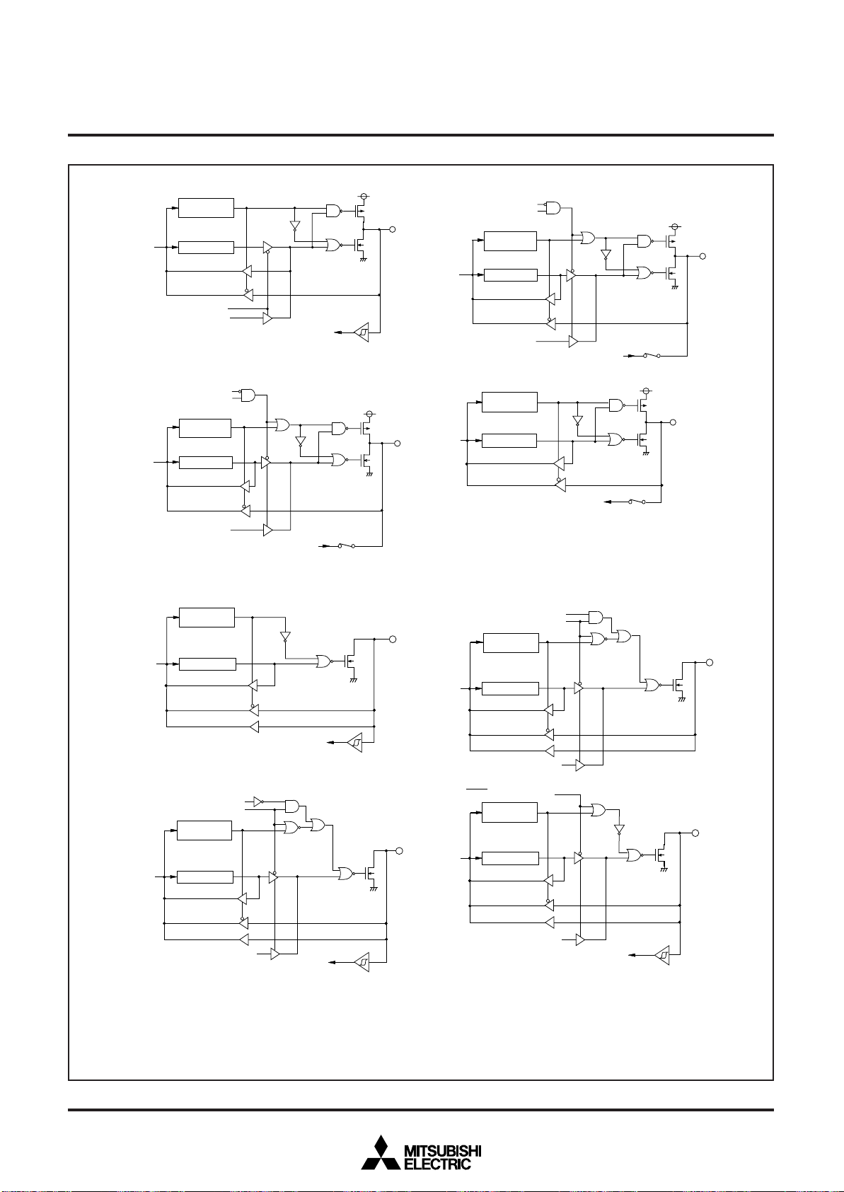
Fig. 12 Port block diagram (3)
16
1 6
) .
1 6
) .
1 6
) .
MITSUBISHI MICROCOMPUTERS
e
t
s
e
t
s
s
3886 Group
SINGLE-CHIP 8-BIT CMOS MICROCOMPUTER
( 2 5 ) P o r t s P 7
D a t a b u
( 2 7 ) P o r t P 7
I2C - B U S i n t e r f a c
D a t a b u
4 ,
P 7
7
e n a b l e b i
5
D i r e c t i o n
r e g i s t e r
P o r t l a t c h
D i r e c t i o n
r e g i s t e r
P o r t l a t c h
S
C L
o u t p u t
I N T
✻4
✻5
3 1
, I N T
4 1
i n t e r r u p t i n p u t
C L
i n p u t
S
( 2 6 ) P o r t P 7
D a t a b u s
( 2 8 ) P o r t P 8
D a t a b u s b u f f e r e n a b l e b i t
D a t a b u
✻6
6
2
I
C - B U S i n t e r f a c
e n a b l e b i
S t a t u s r e g i s t e r 0
S t a t u s r e g i s t e r 1
D i r e c t i o n
r e g i s t e r
P o r t l a t c h
D A
o u t p u t
S
S
0
S
1
R
D i r e c t i o n
r e g i s t e r
P o r t l a t c h
O u t p u t b u f f e r 0
O u t p u t b u f f e r 1
i n p u t
✻6
D A
S
✻6 .
T h e i n p u t l e v e l c a n b e s w i t c h e d b e t w e e n C M O S c o m p a t i b l e i n p u t l e v e l a n d S M B U S l e v e l b y t h e I2C - B U S i n t e r f a c e p i n i n p u t
s e l e c t i o n b i t o f t h e I
2
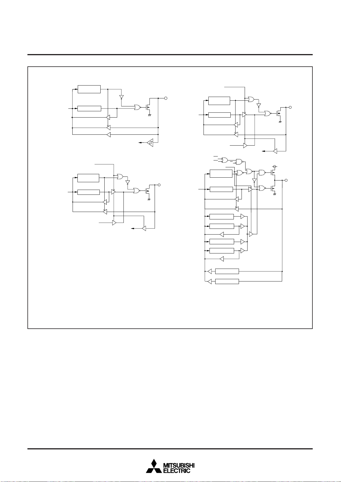
Fig. 13 Port block diagram (4)
C c o n t r o l r e g i s t e r ( a d d r e s s 0 0 1 5
I n p u t b u f f e r 0
I n p u t b u f f e r 1
1 6
) .
✻3
✻3
17
MITSUBISHI MICROCOMPUTERS
3886 Group
SINGLE-CHIP 8-BIT CMOS MICROCOMPUTER
b 7b
0
P o r t c o n t r o l r e g i s t e r 1
1 6
( P C T L 1 : a d d r e s s 0 0 2 E
)
P 00– P 03 o u t p u t s t r u c t u r e s e l e c t i o n b i t
0 : C M O S
1 : N - c h a n n e l o p e n - d r a i n
P 0
4
– P 07 o u t p u t s t r u c t u r e s e l e c t i o n b i t
0 : C M O S
1 : N - c h a n n e l o p e n - d r a i n
P 1
0
– P 13 o u t p u t s t r u c t u r e s e l e c t i o n b i t
0 : C M O S
1 : N - c h a n n e l o p e n - d r a i n
P 1
4
– P 17 o u t p u t s t r u c t u r e s e l e c t i o n b i t
0 : C M O S
1 : N - c h a n n e l o p e n - d r a i n
P 3
0
– P 33 p u l l - u p c o n t r o l b i t
0 : N o p u l l - u p
1 : P u l l - u p
P 3
4
– P 37 p u l l - u p c o n t r o l b i t
0 : N o p u l l - u p
1 : P u l l - u p
P W M
0
e n a b l e b i t
0 : P W M
0
o u t p u t d i s a b l e d
1 : P W M
0
o u t p u t e n a b l e d
P W M
1
e n a b l e b i t
0 : P W M
1
o u t p u t d i s a b l e d
1 : P W M
1
o u t p u t e n a b l e d
b 7b
0
P o r t c o n t r o l r e g i s t e r 2
( P C T L 2 : a d d r e s s 0 0 2 F
1 6
)
Fig. 14 Structure of port I/O related register
P 4 i n p u t l e v e l s e l e c t i o n b i t ( P 42– P 46)
0 : C M O S l e v e l i n p u t
1 : T T L l e v e l i n p u t
P 7 i n p u t l e v e l s e l e c t i o n b i t ( P 7
0
– P 75)
0 : C M O S l e v e l i n p u t
1 : T T L l e v e l i n p u t
P 4 o u t p u t s t r u c t u r e s e l e c t i o n b i t ( P 4
2
, P 43, P 44, P 46)
0 : C M O S
1 : N - c h a n n e l o p e n - d r a i n
P 8 f u n c t i o n s e l e c t i o n b i t
0 : P o r t P 8 / P o r t P 8 d i r e c t i o n r e g i s t e r
1 : P o r t P 4 i n p u t r e g i s t e r / P o r t P 7 i n p u t r e g i s t e r
I N T
2
, I N T3, I N T4 i n t e r r u p t s w i t c h b i t
0 : I N T
2 0
, I N T
3 0
, I N T
4 0
i n t e r r u p t
1 : I N T
2 1
, I N T
3 1
, I N T
4 1
i n t e r r u p t
T i m e r Y c o u n t s o u r c e s e l e c t i o n b i t
0 : f ( X
I N
) / 1 6 ( f ( X
C I N
) / 1 6 i n l o w - s p e e d m o d e )
1 : f ( X
C I N
)
O s c i l l a t i o n s t a b i l i z i n g t i m e s e t a f t e r S T P i n s t r u c t i o n r e l e a s e d b i t
0 : A u t o m a t i c s e t “ 0 1
1 6
” t o t i m e r 1 a n d “ F F
1 6
” t o p r e s c a l e r 1 2
1 : N o a u t o m a t i c s e t
P o r t o u t p u t P 4
2
/ P 43 c l e a r f u n c t i o n s e l e c t i o n b i t
0 : O n l y s o f t w a r e c l e a r
1 : S o f t w a r e c l e a r a n d o u t p u t d a t a b u s b u f f e r 0 r e a d i n g
( s y s t e m b u s s i d e )
18

MITSUBISHI MICROCOMPUTERS
3886 Group
SINGLE-CHIP 8-BIT CMOS MICROCOMPUTER
INTERRUPTS
Interrupts occur by 16 sources among 21 sources: nine external,
eleven internal, and one software.
Interrupt Control
Each interrupt is controlled by an interrupt request bit, an interrupt
enable bit, and the interrupt disable flag except for the software interrupt set by the BRK instruction. An interrupt occurs if the
corresponding interrupt request and enable bits are “1” and the interrupt disable flag is “0”.
Interrupt enable bits can be set or cleared by software.
Interrupt request bits can be cleared by software, but cannot be
set by software.
The BRK instruction cannot be disabled with any flag or bit. The I
(interrupt disable) flag disables all interrupts except the BRK instruction interrupt.
When several interrupts occur at the same time, the interrupts are
received according to priority.
Interrupt Operation
By acceptance of an interrupt, the following operations are automatically performed:
1. The contents of the program counter and the processor status
register are automatically pushed onto the stack.
2. The interrupt disable flag is set and the corresponding interrupt
request bit is cleared.
3. The interrupt jump destination address is read from the vector
table into the program counter.
Interrupt Source Selection
Any of the following interrupt sources can be selected by the interrupt source selection register (address 003916).
1. INT0 or Input buffer full
2. INT1 or Output buffer empty
3. Serial I/O1 transmission or SCLSDA
4. CNTR0 or SCLSDA
5. Serial I/O2 or I2C
6. INT2 or I2C
7. CNTR1 or Key-on wake-up
8. A-D conversion or Key-on wake-up
External Interrupt Pin Selection
The occurrence sources of the external interrupt INT2, INT3, and
INT4 can be selected from either input from INT20, INT30, INT40
pin, or input from INT21, INT31, INT41 pin by the INT2, INT3, INT4
interrupt switch bit (bit 4 of address 002F16).
■ Notes
When setting of the following register or bit is changed, the interrupt request bit may be set to “1.”
• Interrupt edge selection register (address 003A16)
• Interrupt source selection register (address 003916)
• INT2, INT3, INT4 interrupt switch bit of Port control register 2 (bit
4 of address 002F16)
Accept the interrupt after clearing the interrupt request bit to “0”
after interrupt is disabled and the above register or bit is set.
19
Table 6 Interrupt vector addresses and priority
Interrupt Source
Reset (Note 2)
INT0
Input buffer full
(IBF)
INT1
Output buffer
empty (OBE)
Priority
1
2
3
Vector Addresses (Note 1)
High
FFFD16
FFFB16
FFF916
Low
FFFC16
FFFA16
FFF816
MITSUBISHI MICROCOMPUTERS
SINGLE-CHIP 8-BIT CMOS MICROCOMPUTER
Interrupt Request
Generating Conditions
At reset
At detection of either rising or
falling edge of INT0 input
At input data bus buffer writing
At detection of either rising or
falling edge of INT1 input
At output data bus buffer reading
3886 Group
Remarks
Non-maskable
External interrupt
(active edge selectable)
External interrupt
(active edge selectable)
Serial I/O1
reception
Serial I/O1
transmission
SCL, SDA
Timer X
Timer Y
Timer 1
Timer 2
CNTR0
SCL, SDA
CNTR1
Key-on wake-up
Serial I/O2
I2C
INT2
I2C
INT3
INT4
A-D converter
Key-on wake-up
BRK instruction
Notes 1: Vector addresses contain interrupt jump destination addresses.
2: Reset function in the same way as an interrupt with the highest priority.
4
5
6
7
8
9
10
11
12
13
14
15
16
17
FFF716
FFF516
FFF316
FFF116
FFEF16
FFED16
FFEB16
FFE916
FFE716
FFE516
FFE316
FFE116
FFDF16
FFDD16
FFF616
FFF416
FFF216
FFF016
FFEE16
FFEC16
FFEA16
FFE816
FFE616
FFE416
FFE216
FFE016
FFDE16
FFDC16
At completion of serial I/O1 data
reception
At completion of serial I/O1
transfer shift or when transmission buffer is empty
At detection of either rising or
falling edge of SCL or SDA
At timer X underflow
At timer Y underflow
At timer 1 underflow
At timer 2 underflow
At detection of either rising or
falling edge of CNTR0 input
At detection of either rising or
falling edge of SCL or SDA
At detection of either rising or
falling edge of CNTR1 input
At falling of port P3 (at input) input logical level AND
At completion of serial I/O2 data
transfer
At completion of data transfer
At detection of either rising or
falling edge of INT2 input
At completion of data transfer
At detection of either rising or
falling edge of INT3 input
At detection of either rising or
falling edge of INT4 input
At completion of A-D conversion
At falling of port P3 (at input) input logical level AND
At BRK instruction execution
Valid when serial I/O1 is selected
Valid when serial I/O1 is selected
External interrupt
(active edge selectable)
STP release timer underflow
External interrupt
(active edge selectable)
External interrupt
(active edge selectable)
External interrupt
(active edge selectable)
External interrupt (falling valid)
Valid when serial I/O2 is selected
External interrupt
(active edge selectable)
External interrupt
(active edge selectable)
External interrupt
(active edge selectable)
External interrupt (falling valid)
Non-maskable software interrupt
20
t
t
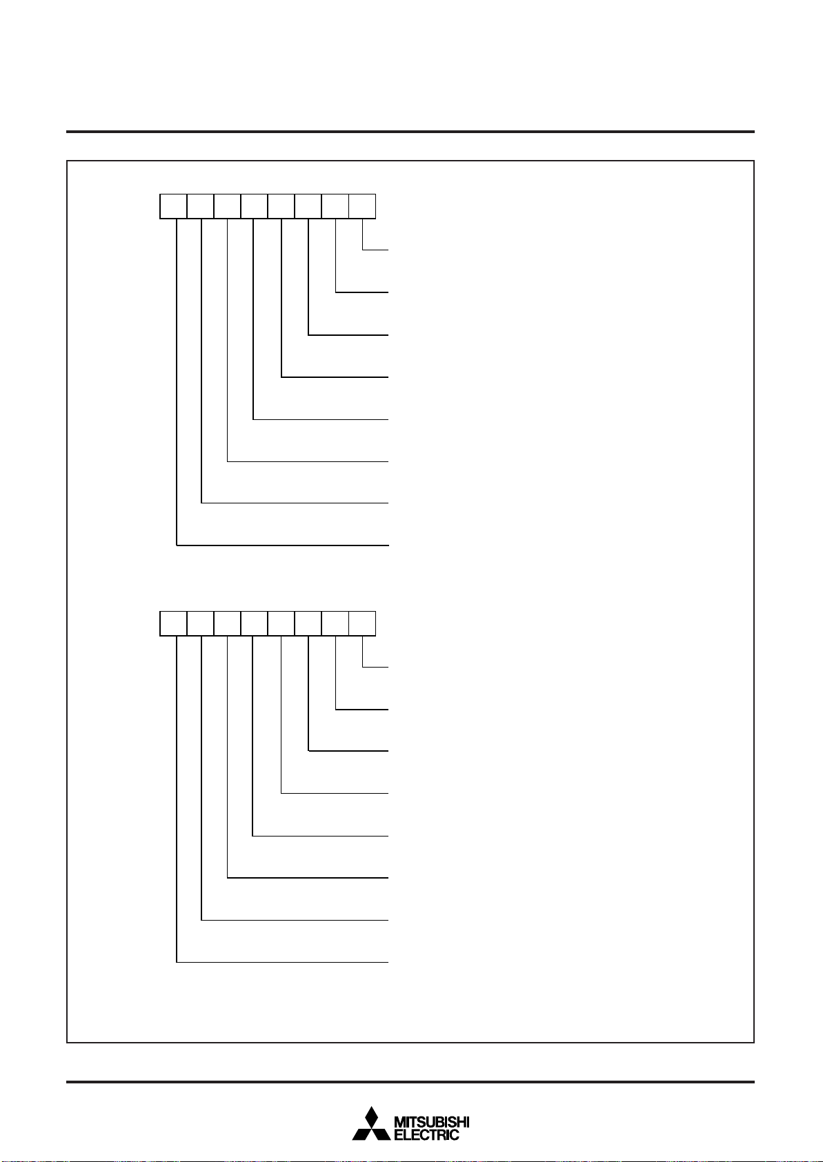
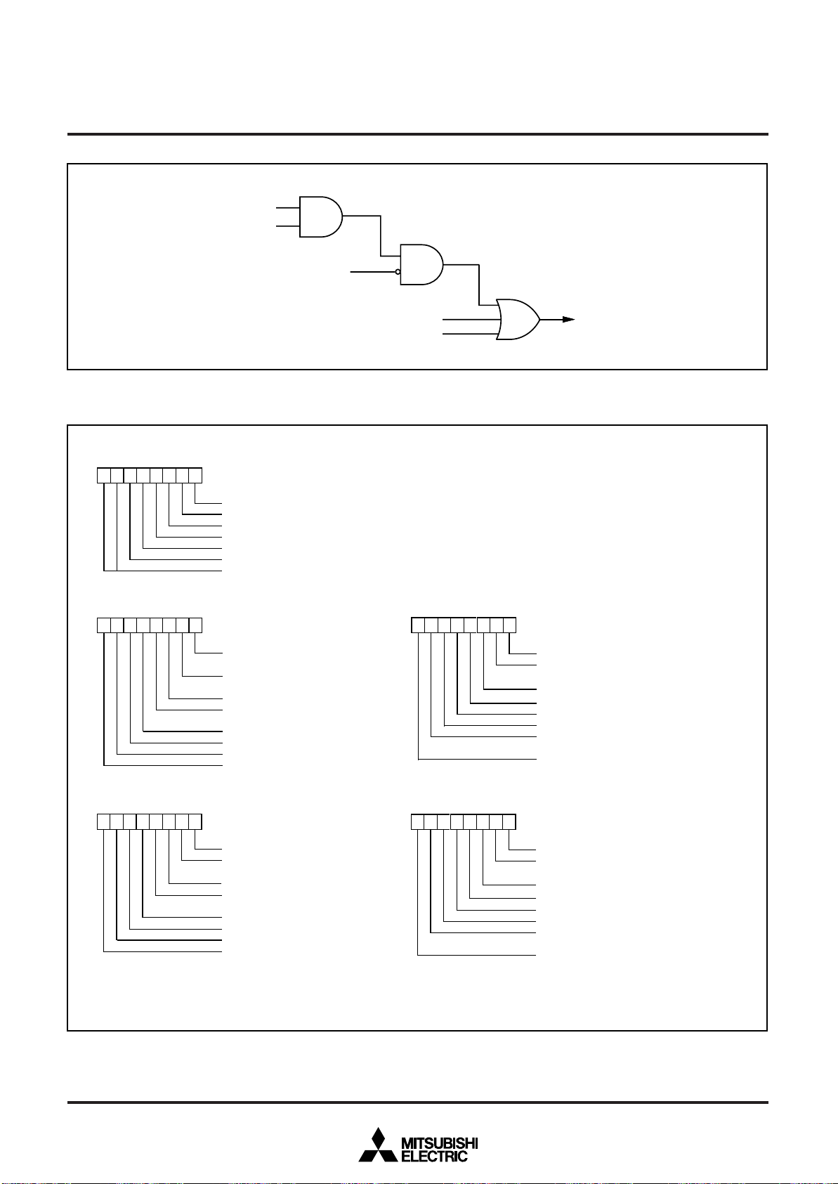
I n t e r r u p t r e q u e s t b i
I n t e r r u p t e n a b l e b i t
I n t e r r u p t d i s a b l e f l a g ( I )
MITSUBISHI MICROCOMPUTERS
3886 Group
SINGLE-CHIP 8-BIT CMOS MICROCOMPUTER
Fig. 15 Interrupt control
b 7 b 0
b 7 b 0
B R K i n s t r u c t i o n
I n t e r r u p t e d g e s e l e c t i o n r e g i s t e r
( I N T E D G E : a d d r e s s 0 0 3 A
I N T0 a c t i v e e d g e s e l e c t i o n b i t
1
a c t i v e e d g e s e l e c t i o n b i t
I N T
N o t u s e d ( r e t u r n s “ 0 ” w h e n r e a d )
2
a c t i v e e d g e s e l e c t i o n b i t
I N T
3
a c t i v e e d g e s e l e c t i o n b i t
I N T
4
a c t i v e e d g e s e l e c t i o n b i t
I N T
N o t u s e d ( r e t u r n s “ 0 ” w h e n r e a d )
I n t e r r u p t r e q u e s t r e g i s t e r 1
( I R E Q 1 : a d d r e s s 0 0 3 C
I N T0/ i n p u t b u f f e r f u l l i n t e r r u p t r e q u e s t
b i t
1
/ o u t p u t b u f f e r e m p t y i n t e r r u p t
I N T
r e q u e s t b i t
S e r i a l I / O 1 r e c e i v e i n t e r r u p t r e q u e s t b i t
S e r i a l I / O 1 t r a n s m i t / S
r e q u e s t b i t
T i m e r X i n t e r r u p t r e q u e s t b i t
T i m e r Y i n t e r r u p t r e q u e s t b i t
T i m e r 1 i n t e r r u p t r e q u e s t b i t
T i m e r 2 i n t e r r u p t r e q u e s t b i t
1 6
)
1 6
)
C L
, S
D A
i n t e r r u p t
R e s e t
0 : F a l l i n g e d g e a c t i v e
1 : R i s i n g e d g e a c t i v e
b 7 b 0
I n t e r r u p t r e q u e s t
I n t e r r u p t r e q u e s t r e g i s t e r 2
( I R E Q 2 : a d d r e s s 0 0 3 D
C N T R0/ S
C N T R
r e q u e s t b i t
S e r i a l I / O 2 / I
I N T
I N T
I N T
A D c o n v e r t e r / k e y - o n w a k e - u p i n t e r r u p t
r e q u e s t b i t
0 : N o i n t e r r u p t r e q u e s t i s s u e d
1 : I n t e r r u p t r e q u e s t i s s u e d
N o t u s e d ( r e t u r n s “ 0 ” w h e n r e a d )
C L
, S
D A
1
2
/ I2C i n t e r r u p t r e q u e s t b i t
3
i n t e r r u p t r e q u e s t b i t
4
i n t e r r u p t r e q u e s t b i t
i n t e r r u p t r e q u e s t b i t
/ k e y - o n w a k e - u p i n t e r r u p t
2
C i n t e r r u p t r e q u e s t b i t
1 6
)
b 7 b 0
I n t e r r u p t c o n t r o l r e g i s t e r 1
( I C O N 1 : a d d r e s s 0 0 3 E
I N T0/ i n p u t b u f f e r f u l l i n t e r r u p t e n a b l e b i
I N T1/ o u t p u t b u f f e r e m p t y i n t e r r u p t
e n a b l e b i t
S e r i a l I / O 1 r e c e i v e i n t e r r u p t e n a b l e b i t
S e r i a l I / O 1 t r a n s m i t / S
e n a b l e b i t
T i m e r X i n t e r r u p t e n a b l e b i t
T i m e r Y i n t e r r u p t e n a b l e b i t
T i m e r 1 i n t e r r u p t e n a b l e b i t
T i m e r 2 i n t e r r u p t e n a b l e b i t
1 6
C L
Fig. 16 Structure of interrupt-related registers (1)
b 7 b 0
)
, S
D A
i n t e r r u p t
I n t e r r u p t c o n t r o l r e g i s t e r 2
( I C O N 2 : a d d r e s s 0 0 3 F
C N T R0/ S
C N T R
e n a b l e b i t
C L
1
/ k e y - o n w a k e - u p i n t e r r u p t
S e r i a l I / O 2 / I
2
/ I2C i n t e r r u p t e n a b l e b i t
I N T
3
i n t e r r u p t e n a b l e b i t
I N T
4
i n t e r r u p t e n a b l e b i t
I N T
A D c o n v e r t e r / k e y - o n w a k e - u p i n t e r r u p t
e n a b l e b i t
N o t u s e d ( r e t u r n s “ 0 ” w h e n r e a d )
0 : I n t e r r u p t s d i s a b l e d
1 : I n t e r r u p t s e n a b l e d
( D o n o t w r i t e “ 1 ” t o t h i s b i t )
1 6
)
, S
D A
i n t e r r u p t e n a b l e b i t
2
C i n t e r r u p t e n a b l e b i t
21
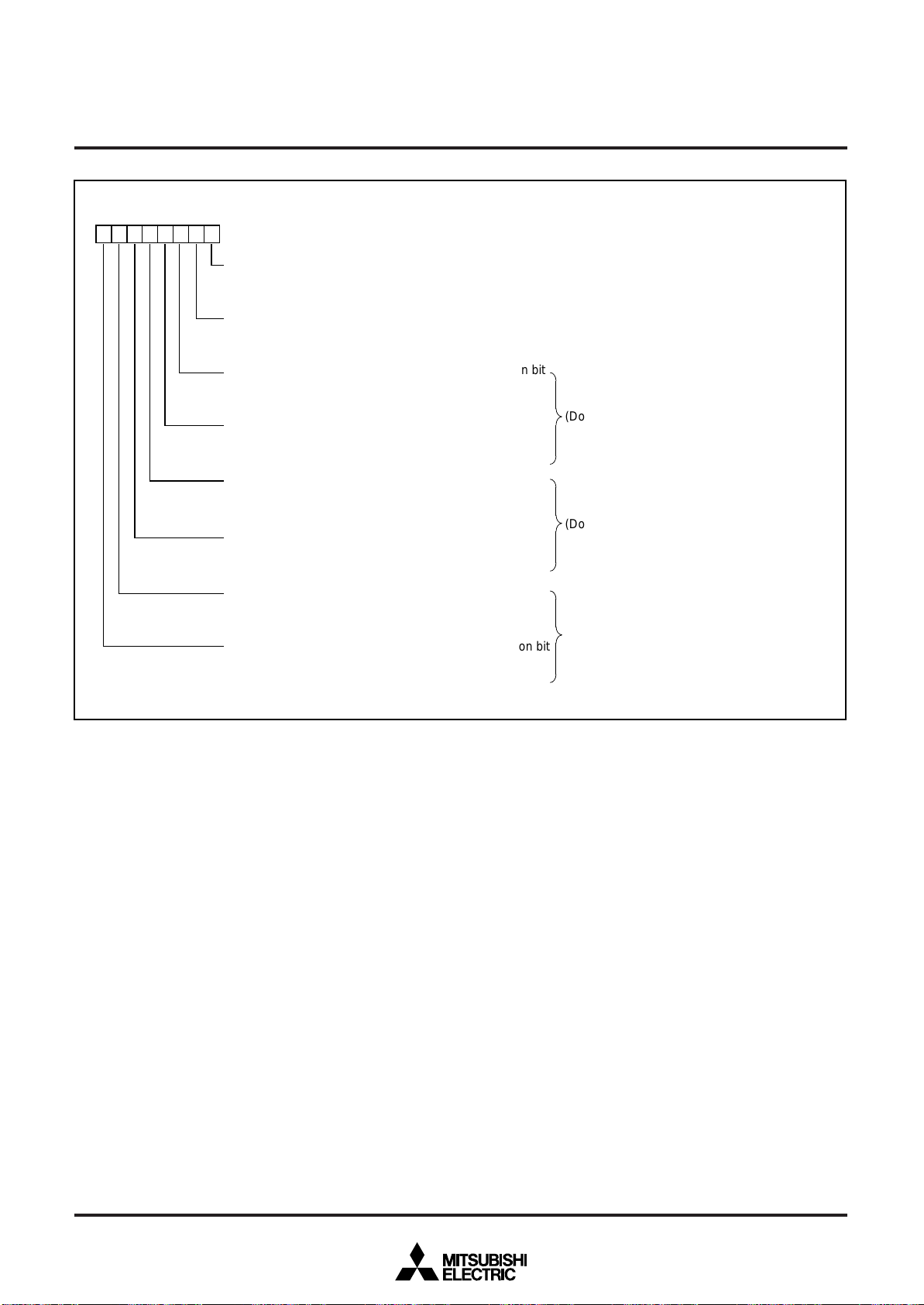
b 7 b 0
I n t e r r u p t s o u r c e s e l e c t i o n r e g i s t e r
( I N T S E L : a d d r e s s 0 0 3 91
o n v e r t e r i n t e r r u p
k e y - o n w a k e - u p i n t e r r u p t s o u r c e s e l e c t i o n b i
n t e r r u p
n t e r r u p
n t e r r u p
n t e r r u p
n t e r r u p
i n t e r r u p t s o u r c e s e l e c t i o n b i
i n t e r r u p t s o u r c e s e l e c t i o n b i
i n t e r r u p
o u t p u t b u f f e r e m p t y i n t e r r u p t s o u r c e s e l e c t i o n b i t
n t e r r u p t
n t e r r u p
I N T0/ i n p u t b u f f e r f u l l i n t e r r u p t s o u r c e s e l e c t i o n b i t
0 i
0 : I N T
6)
t
1 : I n p u t b u f f e r f u l l i n t e r r u p t
MITSUBISHI MICROCOMPUTERS
3886 Group
SINGLE-CHIP 8-BIT CMOS MICROCOMPUTER
1/
I N T
0 : I N T
1 i
1 : O u t p u t b u f f e r e m p t y i n t e r r u p t
S e r i a l I / O 1 t r a n s m i t / S
C L,
0 : S e r i a l I / O 1 t r a n s m i t i n t e r r u p t
1 : S
C L,
SD
A
0/
SC
L,
C N T R
0 : C N T R
1 : S
S e r i a l I / O 2 / I
0 : S e r i a l I / O 2
1 : I
2/
I N T
0 : I N T
1 : I
C N T R
0 : C N T R
SD
0 i
C L,
SD
A i
2
C i n t e r r u p t s o u r c e s e l e c t i o n b i t
2
C i n t e r r u p t
I2C i n t e r r u p t s o u r c e s e l e c t i o n b i t
2 i
2
C i n t e r r u p t
1/
1 i
t
A
t
t
i
t
t
t
1 : K e y - o n w a k e - u p i n t e r r u p t
A D c o n v e r t e r / k e y - o n w a k e - u p i n t e r r u p t s o u r c e s e l e c t i o n b i t
c
0 : A - D
1 : K e y - o n w a k e - u p i n t e r r u p t
Fig. 17 Structure of interrupt-related registers (2)
SD
A
t
t
( D o n o t w r i t e “ 1 ” t o t h e s e b i t s s i m u l t a n e o u s l y . )
( D o n o t w r i t e “ 1 ” t o t h e s e b i t s s i m u l t a n e o u s l y . )
t
( D o n o t w r i t e “ 1 ” t o t h e s e b i t s s i m u l t a n e o u s l y . )
t
22
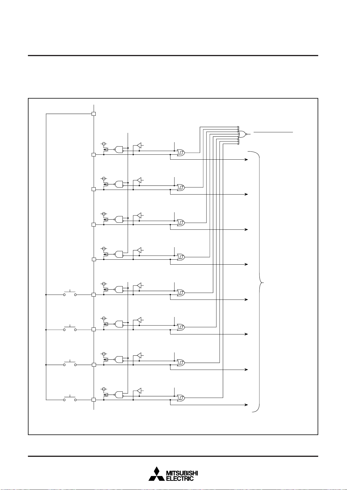
MITSUBISHI MICROCOMPUTERS
3886 Group
SINGLE-CHIP 8-BIT CMOS MICROCOMPUTER
Key Input Interrupt (Key-on Wake Up)
A Key input interrupt request is generated by applying “L” level to
any pin of port P3 that have been set to input mode. In other
words, it is generated when AND of input level goes from “1” to
P o r t P X x
“ L ” l e v e l o u t p u t
P o r t c o n t r o l r e g i s t e r 1
o u t p u
P 3
o u t p u
P 3
o u t p u
P 3
o u t p u
P 3
B i t 5 = “ 1 ”
✻
7
t
✻
6
t
✻
5
t
✻
4
t
✻ ✻
✻ ✻
✻ ✻
✻ ✻
P o r t P 3
d i r e c t i o n r e g i s t e r = “ 1 ”
P o r t P 3 7
l a t c h
P o r t P 3
d i r e c t i o n r e g i s t e r = “ 1 ”
P o r t P 3 6
l a t c h
P o r t P 3 5
l a t c h
P o r t P 3 4
l a t c h
“0”. An example of using a key input interrupt is shown in Figure
18, where an interrupt request is generated by pressing one of the
keys consisted as an active-low key matrix which inputs to ports
P30–P33.
7
6
P o r t P 3
d i r e c t i o n r e g i s t e r = “ 1 ”
P o r t P 3
d i r e c t i o n r e g i s t e r = “ 1 ”
5
4
K e y i n p u t i n t e r r u p t r e q u e s t
i n p u
P 3
n p u
P 3
i n p u
P 3
i n p u
P 3
P o r t c o n t r o l r e g i s t e r 1
B i t 4 = “ 1 ”
✻
3
t
✻
2 i
t
✻
1
t
✻
0
t
✻ ✻
✻ ✻
✻ ✻
✻ ✻
P o r t P 3 3
l a t c h
P o r t P 3 2
l a t c h
P o r t P 3 1
l a t c h
P o r t P 3 0
l a t c h
P o r t P 3
d i r e c t i o n r e g i s t e r = “ 0 ”
P o r t P 3
d i r e c t i o n r e g i s t e r = “ 0 ”
P o r t P 3
d i r e c t i o n r e g i s t e r = “ 0 ”
P o r t P 30
d i r e c t i o n r e g i s t e r = “ 0 ”
3
2
1
Fig. 18 Connection example when using key input interrupt and port P3 block diagram
P o r t P 3
I n p u t r e a d i n g c i r c u i t
C o m p a r a t o r c i r c u i t
✻ P - c h a n n e l t r a n s i s t o r f o r p u l l - u p
✻ ✻ C M O S o u t p u t b u f f e r
23
MITSUBISHI MICROCOMPUTERS
3886 Group
SINGLE-CHIP 8-BIT CMOS MICROCOMPUTER
TIMERS
The 3886 group has four timers: timer X, timer Y, timer 1, and
timer 2.
The division ratio of each timer or prescaler is given by 1/(n + 1),
where n is the value in the corresponding timer or prescaler latch.
All timers are count down. When the timer reaches “0016”, an underflow occurs at the next count pulse and the corresponding
timer latch is reloaded into the timer and the count is continued.
When a timer underflows, the interrupt request bit corresponding
to that timer is set to “1”.
b 7
Fig. 19 Structure of timer XY mode register
b 0
T i m e r X Y m o d e r e g i s t e r
( T M : a d d r e s s 0 0 2 3
T i m e r X o p e r a t i n g m o d e b i t
b 1 b 0
0 0 : T i m e r m o d e
0 1 : P u l s e o u t p u t m o d e
1 0 : E v e n t c o u n t e r m o d e
1 1 : P u l s e w i d t h m e a s u r e m e n t m o d e
C N T R0 a c t i v e e d g e s e l e c t i o n b i t
0 : I n t e r r u p t a t f a l l i n g e d g e
C o u n t a t r i s i n g e d g e i n e v e n t
c o u n t e r m o d e
1 : I n t e r r u p t a t r i s i n g e d g e
C o u n t a t f a l l i n g e d g e i n e v e n t
c o u n t e r m o d e
T i m e r X c o u n t s t o p b i t
0 : C o u n t s t a r t
1 : C o u n t s t o p
T i m e r Y o p e r a t i n g m o d e b i t
b 5 b 4
0 0 : T i m e r m o d e
0 1 : P u l s e o u t p u t m o d e
1 0 : E v e n t c o u n t e r m o d e
1 1 : P u l s e w i d t h m e a s u r e m e n t m o d e
C N T R
1
a c t i v e e d g e s e l e c t i o n b i t
0 : I n t e r r u p t a t f a l l i n g e d g e
C o u n t a t r i s i n g e d g e i n e v e n t
c o u n t e r m o d e
1 : I n t e r r u p t a t r i s i n g e d g e
C o u n t a t f a l l i n g e d g e i n e v e n t
c o u n t e r m o d e
T i m e r Y c o u n t s t o p b i t
0 : C o u n t s t a r t
1 : C o u n t s t o p
1 6
)
Timer 1 and Timer 2
The count source of prescaler 12 is the oscillation frequency divided by 16. The output of prescaler 12 is counted by timer 1 and
timer 2, and a timer underflow sets the interrupt request bit.
Timer X and Timer Y
Timer X and Timer Y can each select in one of four operating
modes by setting the timer XY mode register.
(1) Timer Mode
The timer counts f(XIN)/16.
(2) Pulse Output Mode
Timer X (or timer Y) counts f(XIN)/16. Whenever the contents of
the timer reach “0016”, the signal output from the CNTR0 (or
CNTR1) pin is inverted. If the CNTR0 (or CNTR1) active edge selection bit is “0”, output begins at “ H”.
If it is “1”, output starts at “L”. When using a timer in this mode, set
the corresponding port P54 ( or port P55) direction register to output mode.
(3) Event Counter Mode
Operation in event counter mode is the same as in timer mode,
except that the timer counts signals input through the CNTR0 or
CNTR1 pin.
When the CNTR0 (or CNTR1) active edge selection bit is “0”, the
rising edge of the CNTR0 (or CNTR1) pin is counted.
When the CNTR0 (or CNTR1) active edge selection bit is “1”, the
falling edge of the CNTR0 (or CNTR1) pin is counted.
(4) Pulse Width Measurement Mode
If the CNTR0 (or CNTR1) active edge selection bit is “0”, the timer
counts f(XIN)/16 while the CNTR0 (or CNTR1) pin is at “H”. If the
CNTR0 (or CNTR1) active edge selection bit is “1”, the timer
counts while the CNTR0 (or CNTR1) pin is at “L”.
The count can be stopped by setting “1” to the timer X (or timer Y)
count stop bit in any mode. The corresponding interrupt request
bit is set each time a timer overflows.
The count source for timer Y in the timer mode or the pulse output
mode can be selected from either f(XIN)/16 or f(XCIN) by the timer
Y count source selection bit of the port control register 2 (bit 5 of
address 002F16).
24
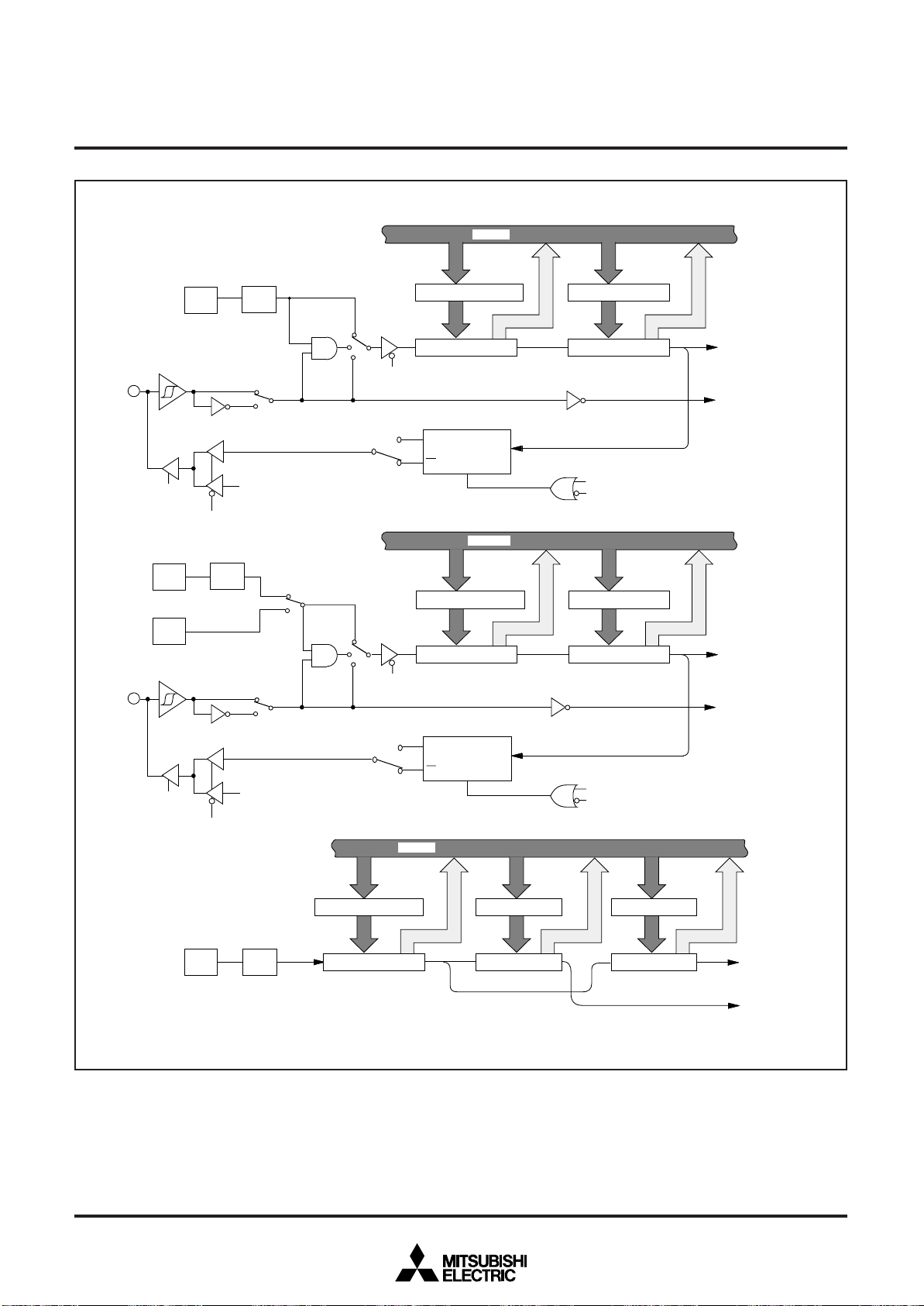
D a t a b u s
MITSUBISHI MICROCOMPUTERS
3886 Group
SINGLE-CHIP 8-BIT CMOS MICROCOMPUTER
( f ( X
4
/ C N T R
P 5
d i r e c t i o n r e g i s t e r
( f ( X
C I N
) i n l o w - s p e e d m o d e )
P 55/ C N T R
d i r e c t i o n r e g i s t e r
O s c i l l a t o r
I N
C I N
) i n l o w - s p e e d m o d e )
0
4
P o r t P 5
P u l s e o u t p u t m o d e
O s c i l l a t o r
I N
)
O s c i l l a t o r
f ( X
C I N
)
1
P o r t P 5
5
P u l s e o u t p u t m o d e
)
D i v i d e r
1 / 1 6f ( X
C N T R
e d g e s e l e c t i o n
b i t
D i v i d e r
1 / 1 6f ( X
0
a c t i v e
C N T R
e d g e s e l e c t i o n
b i t
“ 0 ”
“ 1 ”
P o r t P 5
4
l a t c h
T i m e r Y c o u n t s o u r c e
s e l e c t i o n b i t
“ 0 ”
“ 1 ”
1
a c t i v e
“ 0 ”
“ 1 ”
P o r t P 5 5
l a t c h
P u l s e w i d t h
m e a s u r e m e n t
m o d e
E v e n t
c o u n t e r
m o d e
C N T R
e d g e s e l e c t i o n
b i t
P u l s e w i d t h
m e a s u r e m e n t m o d e
E v e n t
c o u n t e r
m o d e
C N T R
e d g e s e l e c t i o n
b i t
T i m e r m o d e
P u l s e o u t p u t m o d e
T i m e r X c o u n t s t o p b i t
0
a c t i v e
“ 1 ”
“ 0 ”
T i m e r m o d e
P u l s e o u t p u t m o d e
T i m e r Y c o u n t s t o p b i t
1
a c t i v e
“ 1 ”
“ 0 ”
D a t a b u s
P r e s c a l e r X l a t c h ( 8 )
P r e s c a l e r X ( 8 )
Q
T o g g l e f l i p - f l o p
Q
R
D a t a b u s
P r e s c a l e r Y l a t c h ( 8 )
P r e s c a l e r Y ( 8 )
Q
T o g g l e f l i p - f l o p
Q
R
T i m e r X l a t c h ( 8 )
T i m e r X ( 8 )
T o t i m e r X i n t e r r u p t
r e q u e s t b i t
T o C N T R
0
i n t e r r u p t
r e q u e s t b i t
T
T i m e r X l a t c h w r i t e p u l s e
P u l s e o u t p u t m o d e
T i m e r Y l a t c h ( 8 )
T i m e r Y ( 8 )
T o t i m e r Y i n t e r r u p t
r e q u e s t b i t
T o C N T R
1
i n t e r r u p t
r e q u e s t b i t
T
T i m e r Y l a t c h w r i t e p u l s e
P u l s e o u t p u t m o d e
P r e s c a l e r 1 2 l a t c h ( 8 )
D i v i d e rO s c i l l a t o r
P r e s c a l e r 1 2 ( 8 )
( f ( X
C I N
) i n l o w - s p e e d m o d e )
1 / 1 6f ( X
I N
)
Fig. 20 Block diagram of timer X, timer Y, timer 1, and timer 2
T i m e r 1 l a t c h ( 8 )
T i m e r 1 ( 8 )
T i m e r 2 l a t c h ( 8 )
T i m e r 2 ( 8 )
T o t i m e r 2 i n t e r r u p t
r e q u e s t b i t
T o t i m e r 1 i n t e r r u p t
r e q u e s t b i t
25
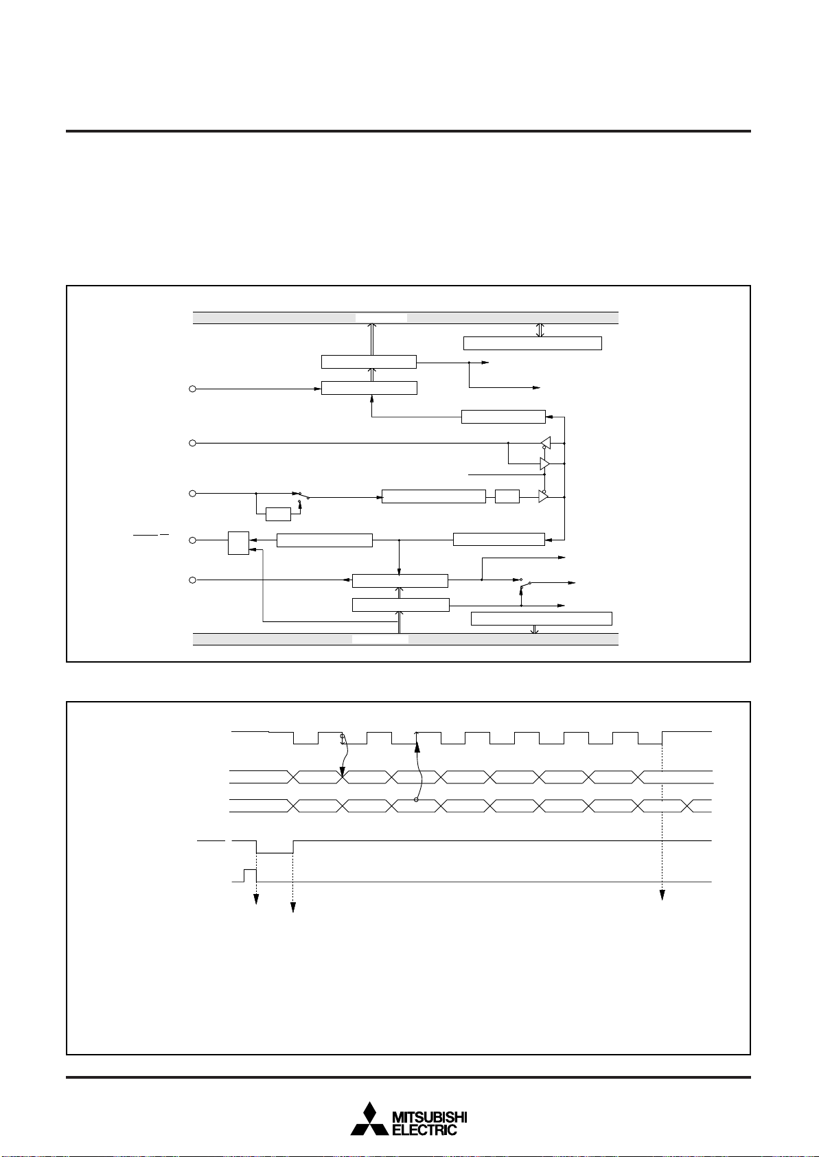
MITSUBISHI MICROCOMPUTERS
r
r
3886 Group
SINGLE-CHIP 8-BIT CMOS MICROCOMPUTER
SERIAL I/O
Serial I/O1
Serial I/O1 can be used as either clock synchronous or asynchronous (UART) serial I/O. A dedicated timer is also provided for
baud rate generation.
D a t a b u s
R e c e i v e b u f f e r r e g i s t e
P 44/ RXD
L K
O B
P 46/ SC
f ( XI
N)
I
i n l o w - s p e e d m o d e
( f ( XC
N)
D Y
P 4
7/
SR
5/
TXD
P 4
1/
F1
0
B R G c o u n t s o u r c e s e l e c t i o n b i t
)
1/
S1
F / F
1 / 4
F a l l i n g - e d g e d e t e c t o r
R e c e i v e s h i f t r e g i s t e r
T r a n s m i t s h i f t r e g i s t e r
T r a n s m i t b u f f e r r e g i s t e r
D a t a b u s
(1) Clock Synchronous Serial I/O Mode
Clock synchronous serial I/O1 mode can be selected by setting
the serial I/O1 mode selection bit of the serial I/O1 control register
(bit 6 of address 001A16) to “1”.
For clock synchronous serial I/O, the transmitter and the receiver
must use the same clock. If an internal clock is used, transfer is
started by a write signal to the TB/RB.
A d d r e s s 0 0 1 81
S h i f t c l o c k
S e r i a l I / O 1 s y n c h r o n o u s
c l o c k s e l e c t i o n b i t
F r e q u e n c y d i v i s i o n r a t i o 1 / ( n + 1 )
B a u d r a t e g e n e r a t o r
A d d r e s s 0 0 1 C
S h i f t c l o c k
A d d r e s s 0 0 1 8
S e r i a l I / O 1 c o n t r o l r e g i s t e r
6
R e c e i v e b u f f e r f u l l f l a g ( R B F )
C l o c k c o n t r o l c i r c u i t
1 / 4
1 6
C l o c k c o n t r o l c i r c u i t
T r a n s m i t i n t e r r u p t s o u r c e s e l e c t i o n b i t
S e r i a l I / O 1 s t a t u s r e g i s t e
1 6
A d d r e s s 0 0 1 A
R e c e i v e i n t e r r u p t r e q u e s t ( R I )
T r a n s m i t s h i f t c o m p l e t i o n f l a g ( T S C )
T r a n s m i t i n t e r r u p t r e q u e s t ( T I )
T r a n s m i t b u f f e r e m p t y f l a g ( T B E )
A d d r e s s 0 0 1 9
1 6
1 6
Fig. 21 Block diagram of clock synchronous serial I/O1
T r a n s f e r s h i f t c l o c k
( 1 / 2 t o 1 / 2 0 4 8 o f t h e i n t e r n a l
c l o c k , o r a n e x t e r n a l c l o c k )
S e r i a l o u t p u t T x D
S e r i a l i n p u t R x D
R e c e i v e e n a b l e s i g n a l S
W r i t e p u l s e t o r e c e i v e / t r a n s m i t
b u f f e r r e g i s t e r ( a d d r e s s 0 0 1 8
N o t e s
1 : A s t h e t r a n s m i t i n t e r r u p t ( T I ) , w h i c h c a n b e s e l e c t e d , e i t h e r w h e n t h e t r a n s m i t b u f f e r h a s e m p t i e d ( T B E = 1 ) o r a f t e r t h e
t r a n s m i t s h i f t o p e r a t i o n h a s e n d e d ( T S C = 1 ) , b y s e t t i n g t h e t r a n s m i t i n t e r r u p t s o u r c e s e l e c t i o n b i t ( T I C ) o f t h e s e r i a l I / O 1
c o n t r o l r e g i s t e r .
2 : I f d a t a i s w r i t t e n t o t h e t r a n s m i t b u f f e r r e g i s t e r w h e n T S C = 0 , t h e t r a n s m i t c l o c k i s g e n e r a t e d c o n t i n u o u s l y a n d s e r i a l d a t a
i s o u t p u t c o n t i n u o u s l y f r o m t h e T x D p i n .
3 : T h e r e c e i v e i n t e r r u p t ( R I ) i s s e t w h e n t h e r e c e i v e b u f f e r f u l l f l a g ( R B F ) b e c o m e s “ 1 ” .
R D Y 1
1 6
)
T B E = 0
T B E = 1
T S C = 0
D
0
D
0
D
1
D
1
Fig. 22 Operation of clock synchronous serial I/O1 function
D
D
2
D
2
D
3
D
3
D
4
D
4
D
5
D
5
D
6
D
6
7
D
7
R B F = 1
T S C = 1
O v e r r u n e r r o r ( O E )
d e t e c t i o n
26
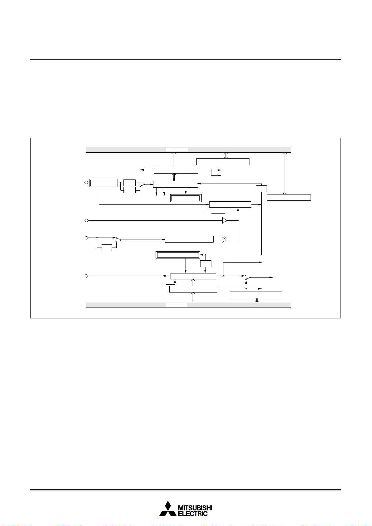
MITSUBISHI MICROCOMPUTERS
r
r
r
3886 Group
SINGLE-CHIP 8-BIT CMOS MICROCOMPUTER
(2) Asynchronous Serial I/O (UART) Mode
Clock asynchronous serial I/O mode (UART) can be selected by
clearing the serial I/O1 mode selection bit of the serial I/O1 control
register to “0”.
Eight serial data transfer formats can be selected, and the transfer
formats used by a transmitter and receiver must be identical.
The transmit and receive shift registers each have a buffer, but the
D a t a b u s
P 4
4
/ RXD
P 46/ S
C L K 1
/ O B F
f ( X
I N
)
( f ( X
C I N
) i n l o w - s p e e d m o d e )
5
/ TXD
P 4
A d d r e s s 0 0 1 8
O E
C h a r a c t e r l e n g t h s e l e c t i o n b i t
S T d e t e c t o r
1 0
B R G c o u n t s o u r c e s e l e c t i o n b i t
1 / 4
7 b i t s
8 b i t s
S e r i a l I / O 1 s y n c h r o n o u s c l o c k s e l e c t i o n b i t
C h a r a c t e r l e n g t h s e l e c t i o n b i t
1 6
R e c e i v e b u f f e r r e g i s t e r
R e c e i v e s h i f t r e g i s t e
P EF E
F r e q u e n c y d i v i s i o n r a t i o 1 / ( n + 1 )
B a u d r a t e g e n e r a t o r
S T / S P / P A g e n e r a t o r
T r a n s m i t s h i f t r e g i s t e r
T r a n s m i t b u f f e r r e g i s t e
D a t a b u s
two buffers have the same address in memory. Since the shift register cannot be written to or read from directly, transmit data is
written to the transmit buffer register, and receive data is read
from the receive buffer register.
The transmit buffer register can also hold the next data to be
transmitted, and the receive buffer register can hold a character
while the next character is being received.
S P d e t e c t o r
A d d r e s s 0 0 1 C
S e r i a l I / O 1 c o n t r o l r e g i s t e
R e c e i v e b u f f e r f u l l f l a g ( R B F )
R e c e i v e i n t e r r u p t r e q u e s t ( R I )
C l o c k c o n t r o l c i r c u i t
1 6
1 / 1 6
T r a n s m i t i n t e r r u p t s o u r c e s e l e c t i o n b i t
A d d r e s s
0 0 1 8
S e r i a l I / O 1 s t a t u s r e g i s t e r
1 6
A d d r e s s 0 0 1 A
1 / 1 6
1 6
U A R T c o n t r o l r e g i s t e r
A d d r e s s 0 0 1 B
T r a n s m i t s h i f t c o m p l e t i o n f l a g ( T S C )
T r a n s m i t i n t e r r u p t r e q u e s t ( T I )
T r a n s m i t b u f f e r e m p t y f l a g ( T B E )
A d d r e s s
0 0 1 9
1 6
1 6
Fig. 23 Block diagram of UART serial I/O1
27
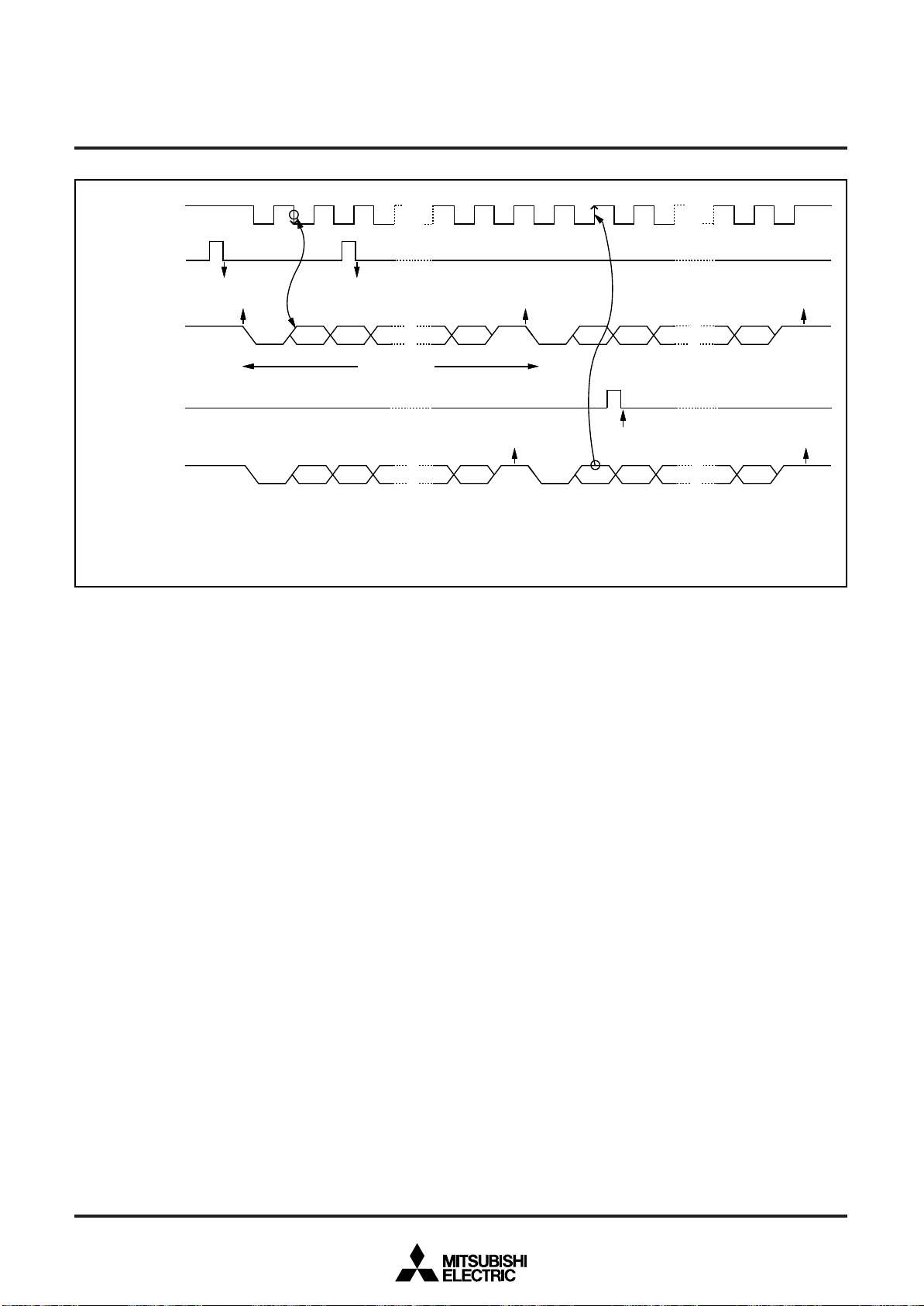
T
T
T
T
k
T r a n s m i t o r r e c e i v e c l o c
MITSUBISHI MICROCOMPUTERS
3886 Group
SINGLE-CHIP 8-BIT CMOS MICROCOMPUTER
T r a n s m i t b u f f e r w r i t e
R e c e i v e b u f f e r r e a d
s i g n a l
T B E = 0T
T S C = 0
T B E = 1
S e r i a l o u t p u t TXD
s i g n a l
S e r i a l i n p u t RXD
N o t e s
1 : E r r o r f l a g d e t e c t i o n o c c u r s a t t h e s a m e t i m e t h a t t h e R B F f l a g b e c o m e s “ 1 ” ( a t 1 s t s t o p b i t , d u r i n g r e c e p t i o n ) .
2 : A s t h e t r a n s m i t i n t e r r u p t ( T I ) , w h e n e i t h e r t h e T B E o r T S C f l a g b e c o m e s “ 1 , ” c a n b e s e l e c t e d t o o c c u r d e p e n d i n g o n t h e s e t t i n g o f t h e t r a n s m i t
i n t e r r u p t s o u r c e s e l e c t i o n b i t ( T I C ) o f t h e s e r i a l I / O 1 c o n t r o l r e g i s t e r .
3 : T h e r e c e i v e i n t e r r u p t ( R I ) i s s e t w h e n t h e R B F f l a g b e c o m e s “ 1 . ”
4 : A f t e r d a t a i s w r i t t e n t o t h e t r a n s m i t b u f f e r w h e n T S C = 1 , 0 . 5 t o 1 . 5 c y c l e s o f t h e d a t a s h i f t c y c l e i s n e c e s s a r y u n t i l c h a n g i n g t o T S C = 0 .
S
S
B E =
0
D0 D1
1 s t a r t b i t
7 o r 8 d a t a b i t
1 o r 0 p a r i t y b i t
1 o r 2 s t o p b i t ( s )
D0 D1 S P D0 D1
Fig. 24 Operation of UART serial I/O1 function
[Serial I/O1 Control Register (SIO1CON)]
16
001A
The serial I/O1 control register consists of eight control bits for the
serial I/O function.
[UART Control Register (UARTCON)] 001B16
The UART control register consists of four control bits (bits 0 to 3)
which are valid when asynchronous serial I/O is selected and set
the data format of an data transfer and one bit (bit 4) which is always valid and sets the output structure of the P45/TXD pin.
[Serial I/O1 Status Register (SIO1STS)]
16
0019
The read-only serial I/O1 status register consists of seven flags
(bits 0 to 6) which indicate the operating status of the serial I/O
function and various errors.
Three of the flags (bits 4 to 6) are valid only in UART mode.
The receive buffer full flag (bit 1) is cleared to “0” when the receive
buffer register is read.
If there is an error, it is detected at the same time that data is
transferred from the receive shift register to the receive buffer register, and the receive buffer full flag is set. A write to the serial I/O1
status register clears all the error flags OE, PE, FE, and SE (bit 3
to bit 6, respectively). Writing “0” to the serial I/O1 enable bit SIOE
(bit 7 of the serial I/O control register) also clears all the status
flags, including the error flags.
Bits 0 to 6 of the serial I/O1 status register are initialized to “0” at
reset, but if the transmit enable bit (bit 4) of the serial I/O1 control
register has been set to “1”, the transmit shift completion flag (bit
2) and the transmit buffer empty flag (bit 0) become “1”.
T B E = 1
S P
R B F = 1
S
S
D0 D1
R B F = 0
✽
G e n e r a t e d a t 2 n d b i t i n 2 - s t o p - b i t m o d e
T S C = 1
S P
R B F = 1
S P
✽
[Transmit Buffer Register/Receive Buffer
Register (TB/RB)] 0018
The transmit buffer register and the receive buffer register are located at the same address. The transmit buffer is write-only and
the receive buffer is read-only. If a character bit length is 7 bits, the
MSB of data stored in the receive buffer is “0”.
16
[Baud Rate Generator (BRG)] 001C16
The baud rate generator determines the baud rate for serial transfer.
The baud rate generator divides the frequency of the count source
by 1/(n + 1), where n is the value written to the baud rate generator.
28
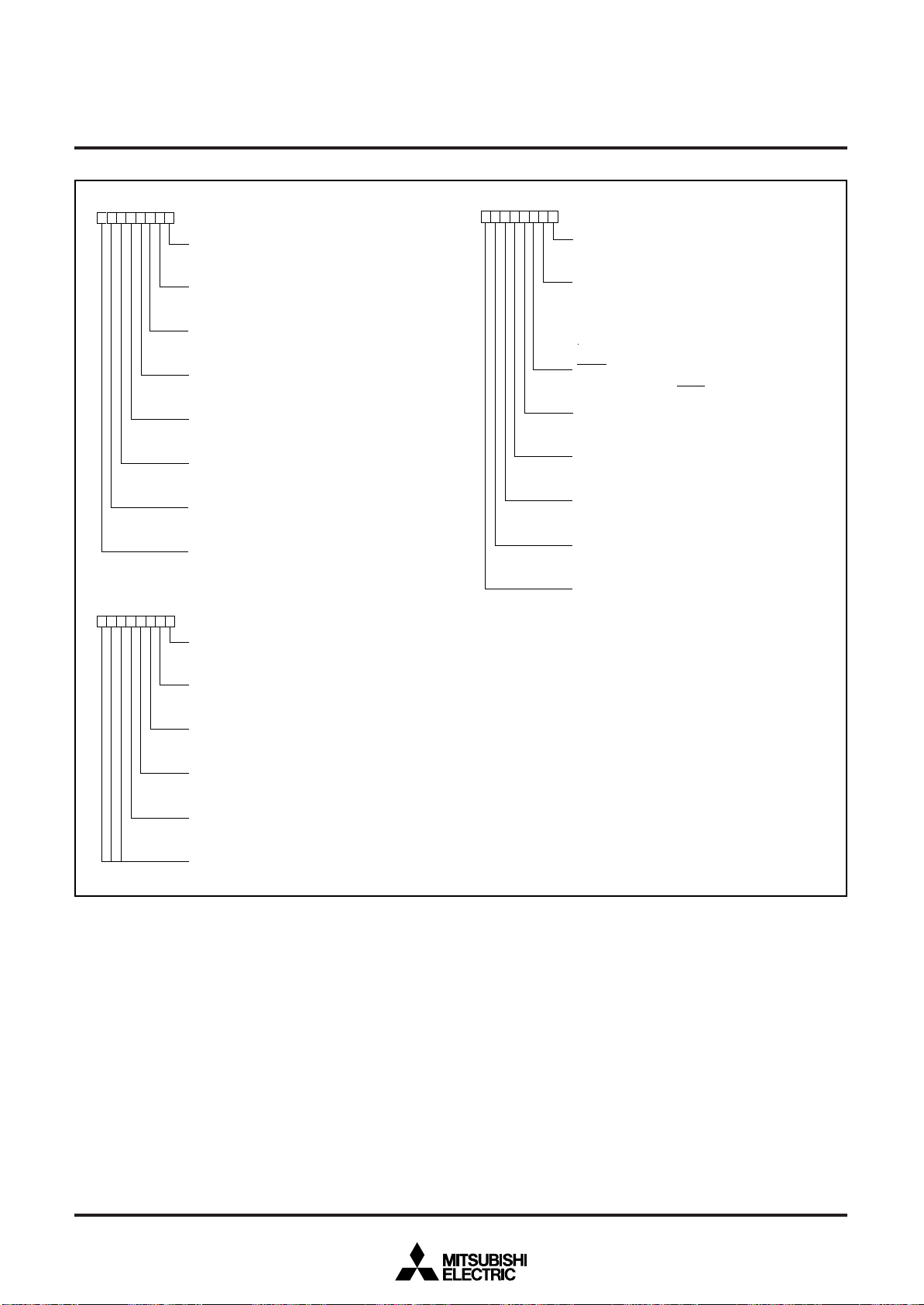
MITSUBISHI MICROCOMPUTERS
3886 Group
SINGLE-CHIP 8-BIT CMOS MICROCOMPUTER
b 7
b 0
S e r i a l I / O 1 s t a t u s r e g i s t e r
( S I O 1 S T S : a d d r e s s 0 0 1 9
T r a n s m i t b u f f e r e m p t y f l a g ( T B E )
0 : B u f f e r f u l l
1 : B u f f e r e m p t y
R e c e i v e b u f f e r f u l l f l a g ( R B F )
0 : B u f f e r e m p t y
1 : B u f f e r f u l l
T r a n s m i t s h i f t c o m p l e t i o n f l a g ( T S C )
0 : T r a n s m i t s h i f t i n p r o g r e s s
1 : T r a n s m i t s h i f t c o m p l e t e d
O v e r r u n e r r o r f l a g ( O E )
0 : N o e r r o r
1 : O v e r r u n e r r o r
P a r i t y e r r o r f l a g ( P E )
0 : N o e r r o r
1 : P a r i t y e r r o r
F r a m i n g e r r o r f l a g ( F E )
0 : N o e r r o r
1 : F r a m i n g e r r o r
S u m m i n g e r r o r f l a g ( S E )
0 : ( O E ) U ( P E ) U ( F E ) = 0
1 : ( O E ) U ( P E ) U ( F E ) = 1
1 6
)
b 7
N o t u s e d ( r e t u r n s “ 1 ” w h e n r e a d )
b 7
b 0
U A R T c o n t r o l r e g i s t e r
( U A R T C O N : a d d r e s s 0 0 1 B
C h a r a c t e r l e n g t h s e l e c t i o n b i t ( C H A S )
0 : 8 b i t s
1 : 7 b i t s
P a r i t y e n a b l e b i t ( P A R E )
0 : P a r i t y c h e c k i n g d i s a b l e d
1 : P a r i t y c h e c k i n g e n a b l e d
P a r i t y s e l e c t i o n b i t ( P A R S )
0 : E v e n p a r i t y
1 : O d d p a r i t y
S t o p b i t l e n g t h s e l e c t i o n b i t ( S T P S )
0 : 1 s t o p b i t
1 : 2 s t o p b i t s
5
/ TXD P - c h a n n e l o u t p u t d i s a b l e b i t ( P O F F )
P 4
0 : C M O S o u t p u t ( i n o u t p u t m o d e )
1 : N - c h a n n e l o p e n d r a i n o u t p u t ( i n o u t p u t m o d e )
1 6
)
b 0
S e r i a l I / O 1 c o n t r o l r e g i s t e r
( S I O 1 C O N : a d d r e s s 0 0 1 A
B R G c o u n t s o u r c e s e l e c t i o n b i t ( C S S )
I N
) ( f ( X
0 : f ( X
1 : f ( X
S e r i a l I / O 1 s y n c h r o n o u s c l o c k s e l e c t i o n b i t ( S C S )
0 : B R G o u t p u t d i v i d e d b y 4 w h e n c l o c k s y n c h r o n o u s
s e r i a l I / O i s s e l e c t e d , B R G o u t p u t d i v i d e d b y 1 6
w h e n U A R T i s s e l e c t e d .
1 : E x t e r n a l c l o c k i n p u t w h e n c l o c k s y n c h r o n o u s s e r i a l
I / O i s s e l e c t e d , e x t e r n a l c l o c k i n p u t d i v i d e d b y 1 6
w h e n U A R T i s s e l e c t e d .
R D Y 1
S
0 : P 4
1 : P 4
T r a n s m i t i n t e r r u p t s o u r c e s e l e c t i o n b i t ( T I C )
0 : I n t e r r u p t w h e n t r a n s m i t b u f f e r h a s e m p t i e d
1 : I n t e r r u p t w h e n t r a n s m i t s h i f t o p e r a t i o n i s c o m p l e t e d
T r a n s m i t e n a b l e b i t ( T E )
0 : T r a n s m i t d i s a b l e d
1 : T r a n s m i t e n a b l e d
R e c e i v e e n a b l e b i t ( R E )
0 : R e c e i v e d i s a b l e d
1 : R e c e i v e e n a b l e d
S e r i a l I / O 1 m o d e s e l e c t i o n b i t ( S I O M )
0 : C l o c k a s y n c h r o n o u s ( U A R T ) s e r i a l I / O
1 : C l o c k s y n c h r o n o u s s e r i a l I / O
S e r i a l I / O 1 e n a b l e b i t ( S I O E )
0 : S e r i a l I / O d i s a b l e d
( p i n s P 4
1 : S e r i a l I / O e n a b l e d
( p i n s P 4
C I N
I N
) / 4 ( f ( X
o u t p u t e n a b l e b i t ( S R D Y )
7
p i n o p e r a t e s a s o r d i n a r y I / O p i n
7
p i n o p e r a t e s a s S
4
t o P 47 o p e r a t e a s o r d i n a r y I / O p i n s )
4
t o P 47 o p e r a t e a s s e r i a l I / O p i n s )
1 6
)
) i n l o w - s p e e d m o d e )
C I N
) / 4 i n l o w - s p e e d m o d e )
R D Y 1
o u t p u t p i n
N o t u s e d ( r e t u r n “ 1 ” w h e n r e a d )
Fig. 25 Structure of serial I/O1 control registers
29
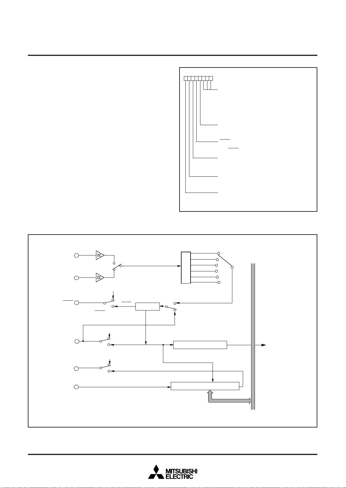
MITSUBISHI MICROCOMPUTERS
3886 Group
SINGLE-CHIP 8-BIT CMOS MICROCOMPUTER
Serial I/O2
The serial I/O2 function can be used only for clock synchronous
serial I/O.
For clock synchronous serial I/O the transmitter and the receiver
must use the same clock. If the internal clock is used, transfer is
started by a write signal to the serial I/O2 register.
[Serial I/O2 Control Register (SIO2CON)]
16
001D
The serial I/O2 control register contains seven bits which control
various serial I/O functions.
b 7
b 0
S e r i a l I / O 2 c o n t r o l r e g i s t e r
( S I O 2 C O N : a d d r e s s 0 0 1 D
P
i n p u
s i g n a l o u t p u
o u t p u t e n a b l e b i t
s i g n a l o u t p u
/ 2 5 6 ( f (
/ 2 5 6 i n l o w - s p e e d m o d e
/ 1 2 8 ( f (
/ 1 2 8 i n l o w - s p e e d m o d e
/ 3 2 ( f (
/ 3 2 i n l o w - s p e e d m o d e
/ 6 4 ( f (
/ 6 4 i n l o w - s p e e d m o d e
/ 1 6 ( f (
/ 1 6 i n l o w - s p e e d m o d e
/ 8 ( f (
/ 8 i n l o w - s p e e d m o d e
I
I
I
I
I
I
E
L K
I n t e r n a l s y n c h r o n o u s c l o c k s e l e c t i o n b i t s
b 2 b 1 b 0
0 0 0 : f ( XI
N)
I N)
0 0 1 : f ( X
I N)
0 1 0 : f ( X
0 1 1 : f ( X
I N)
I N)
1 1 0 : f ( X
I N)
1 1 1 : f ( X
S e r i a l I / O 2 p o r t s e l e c t i o n b i t
0 : I / O p o r t
O U T 2,
SC
1 : S
R D Y 2
S
0 : I / O p o r t
R D Y 2
1 : S
T r a n s f e r d i r e c t i o n s e l e c t i o n b i t
0 : L S B f i r s t
1 : M S B f i r s t
S e r i a l I / O 2 s y n c h r o n o u s c l o c k s e l e c t i o n b i t
0 : E x t e r n a l c l o c k
1 : I n t e r n a l c l o c k
C o m p a r a t o r r e f e r e n c e i n p u t s e l e c t i o n b i t
0/
3R
0 : P 0
1 : R e f e r e n c e i n p u t f i x e d
F
1 6)
XC
N)
XC
N)
XC
N)
XC
N)
XC
N)
XC
N)
2
t
t
t
Fig. 26 Structure of serial I/O2 control register
)
)
)
)
)
)
X
C I N
M a i n c l o c k d i v i d e r a t i o
s e l e c t i o n b i t s ( N o t e )
X
I N
P 7
3
/ S
R D Y 2
/ I N T
2 1
P 72/ S
C L K 2
S e r i a l I / O 2 p o r t s e l e c t i o n b i t
P 71/ S
O U T 2
S e r i a l I / O 2 p o r t s e l e c t i o n b i t
P 70/ S
I N 2
N o t e :
T h e s e a r e a s s i g n e d t o b i t s 7 a n d 6 o f t h e C P U m o d e r e g i s t e r ( a d d r e s s 0 0 3 B
T h e s e b i t s s e l e c t a n y o f t h e h i g h - s p e e d m o d e , t h e m i d d l e - s p e e d m o d e , a n d t h e l o w - s p e e d m o d e .
R D Y 2
S
“ 1 0 ”
“ 0 0 ”
“ 0 1 ”
3
l a t c h
P 7
“ 0 ”
S
“ 1 ”
o u t p u t e n a b l e b i t
P 7
2
l a t c h
“ 0 ”
“ 1 ”
P 7
1
l a t c h
“ 0 ”
“ 1 ”
S e r i a l I / O 2 s y n c h r o n o u s
R D Y 2
c l o c k s e l e c t i o n b i t
S y n c h r o n i z a t i o n
c i r c u i t
2
C
S
L K
E x t e r n a l c l o c k
r
D
i v i d e
“ 1 ”
“ 0 ”
S e r i a l I / O c o u n t e r 2 ( 3 )
S e r i a l I / O 2 r e g i s t e r ( 8 )
1 6
) .
1 / 8
1 / 1 6
1 / 3 2
1 / 6 4
1 / 1 2 8
1 / 2 5 6
I n t e r n a l s y n c h r o n o u s
c l o c k s e l e c t i o n b i t s
D a t a b u s
S e r i a l I / O 2
i n t e r r u p t r e q u e s t
Fig. 27 Block diagram of serial I/O2 function
30

T r a n s f e r c l o c k ( N o t e 1 )
r
S e r i a l I / O 2 r e g i s t e
w r i t e s i g n a l
S e r i a l I / O 2 o u t p u t S
N
S e r i a l I / O 2 i n p u t SI
D Y
R e c e i v e e n a b l e s i g n a l SR
p i n g o e s t o h i g h i m p e d a n c e a f t e r t r a n s f e r c o m p l e t i o n
N o t e s
1 : W h e n t h e i n t e r n a l c l o c k i s s e l e c t e d a s t h e t r a n s f e r c l o c k , t h e d i v i d e r a t i o c a n b e s e l e c t e d b y s e t t i n g b i t s 0 t o 2 o f t h e s e r i a l
I / O 2 c o n t r o l r e g i s t e r .
2 : W h e n t h e i n t e r n a l c l o c k i s s e l e c t e d a s t h e t r a n s f e r c l o c k , t h e S
O U T 2
MITSUBISHI MICROCOMPUTERS
3886 Group
SINGLE-CHIP 8-BIT CMOS MICROCOMPUTER
( N o t e 2 )
D2
2
2
D3 D4 D5 D6
S e r i a l I / O 2 i n t e r r u p t r e q u e s t b i t s e t
O U T 2
D7D0 D1
.
Fig. 28 Timing of serial I/O2 function
31

MITSUBISHI MICROCOMPUTERS
3886 Group
SINGLE-CHIP 8-BIT CMOS MICROCOMPUTER
PULSE WIDTH MODULATION (PWM) OUTPUT CIRCUIT
The 3886 group has two PWM output circuits, PWM0 and PWM1,
with 14-bit resolution respectively. These can operate independently. When the oscillation frequency XIN is 10 MHz, the
minimum resolution bit width is 200 ns and the cycle period is
3276.8 µs. The PWM timing generator supplies a PWM control
signal based on a signal that is the frequency of the XIN clock.
D a t a B u s
S e t t o “ 1 ”
a t w r i t e
b i t 7
b i t 7
b i t 0
P W M 0 H r e g i s t e r
( a d d r e s s 0 0 3 0
1 6)
The following explanation assumes f(XIN) = 8 MHz.
P W M 0 L r e g i s t e r ( a d d r e s s 0 0 3 11
b i t 5
b i t 0
6)
P W M 0 l a t c h ( 1 4 b i t s )
M S B L S B
1 4
1 4 - b i t P W M 0 c i r c u i t
u t p u t s e l e c t i o n b i
P W M0
f ( XI
( 8 M H z )
N)
1 / 2
( 4 M H z )
t i m i n g
g e n e r a t o r
P W M 0
( 6 4 µs p e r i o d )
( 4 0 9 6 µs p e r i o d )
u t p u t s e l e c t i o n b i
P W M0
P W M0
o
n a b l e b i
P W M0
o
n a b l e b i
0 e
P W M
P 56 d i r e c t i o n r e g i s t e r
t
e
t
P 30 d i r e c t i o n r e g i s t e r
t
t
n a b l e b i
P W M0
n a b l e b i
P W M
a t c
0 l
h
P 3
e
t
l a t c
6
h
P 5
0 e
t
P W
P 3
D
P 5
0/
6/
M0
0
A1/ P W M0
1
Fig. 29 PWM block diagram (PWM0)
32

MITSUBISHI MICROCOMPUTERS
3886 Group
SINGLE-CHIP 8-BIT CMOS MICROCOMPUTER
Data Setup (PWM0)
The PWM0 output pin also functions as port P30 or P56. The
PWM0 output pin is selected from either P30/PWM00 or
P56/PWM01 by bit 4 of the AD/DA control register (address
003416).
The PWM0 output becomes enabled state by setting bit 6 of the
port control register 1 (address 002E16). The high-order eight bits
of output data are set in the PWM0H register (address 003016)
and the low-order six bits are set in the PWM0L register (address
003116).
PWM1 is set as the same way.
PWM Operation
The 14-bit PWM data is divided into the low-order six bits and the
high-order eight bits in the PWM latch.
The high-order eight bits of data determine how long an “H”-level
signal is output during each sub-period. There are 64 sub-periods
in each period, and each sub-period is 256 ✕ τ (64 µs) long. The
signal is “H” for a length equal to N times τ, where τ is the mini-
Table 7 Relationship between low-order 6 bits of data and
period set by the ADD bit
Low-order 6 bits of data (PWML)
000000
000001
000010
000100
001000
010000
100000
Sub-periods tm Lengthened (m=0 to 63)
LSB
None
m=32
m=16, 48
m=8, 24, 40, 56
m=4, 12, 20, 28, 36, 44, 52, 60
m=2, 6, 10, 14, 18, 22, 26, 30, 34, 38, 42, 46, 50, 54, 58, 62
m=1, 3, 5, 7, ................................................ ,57, 59, 61, 63
mum resolution (250 ns).
“H” or “L” of the bit in the ADD part shown in Figure 30 is added to
this “H” duration by the contents of the low-order 6-bit data according to the rule in Table 7.
That is, only in the sub-period tm shown by Table 7 in the PWM
cycle period T = 64t, its “H” duration is lengthened to the minimum
resolution τ added to the length of other periods.
For example, if the high-order eight bits of the 14-bit data are 0316
and the low-order six bits are 0516, the length of the “H”-level output in sub-periods t8, t24, t32, t40, and t56 is 4 τ, and its length is 3
τ in all other sub-periods.
Time at the “H” level of each sub-period almost becomes equal,
because the time becomes length set in the high-order 8 bits or
becomes the value plus τ, and this sub-period t (= 64 µs, approximate 15.6 kHz) becomes cycle period approximately.
Transfer From Register to Latch
Data written to the PWML register is transferred to the PWM latch
at each PWM period (every 4096 µs), and data written to the
PWMH register is transferred to the PWM latch at each sub-period
(every 64 µs). The signal which is output to the PWM output pin is
corresponding to the contents of this latch. When the PWML register is read, the latch contents are read. However, bit 7 of the
PWML register indicates whether the transfer to the PWM latch is
completed; the transfer is completed when bit 7 is “0” and it is not
done when bit 7 is “1.”
1 5 . 7 5 µs 1 5 . 7 5 µs 1 5 . 7 5 µs 1 6 . 0 µs 1 5 . 7 5 µs
P u l s e w i d t h m o d u l a t i o n r e g i s t e r H
P u l s e w i d t h m o d u l a t i o n r e g i s t e r L
S u b - p e r i o d s w h e r e “ H ” p u l s e w i d t h i s 1 6 . 0 µs :
S u b - p e r i o d s w h e r e “ H ” p u l s e w i d t h i s 1 5 . 7 5 µs :
Fig. 30 PWM timing
6 4 µs
m = 0
4 0 9 6 µs
6 4 µs
m = 7m
: 0 0 1 1 1 1 1 1
: 0 0 0 1 0 1
6 4 µs
m = 8
6 4 µs
=
9m
1 5 . 7 5 µs
m = 8 , 2 4 , 3 2 , 4 0 , 5 6
m = a l l o t h e r v a l u e s
1 5 . 7 5 µs
6 4 µs
= 6
3
33

P W M 0 H
r e g i s t e r
P W M 0 L
r e g i s t e r
P W M 0 l a t c h
( 1 4 b i t s )
E x a m p l e 1
P W M
0
o u t p u t
5 9
1 6
D a t a 2 4
1 3
1 6
1 6 5 3
6 A 6 A6
1
D a t a 6 A
1 6
s t o r e d a t a d d r e s s 0 0 3 0
6 A
1 6
s t o r e d a t a d d r e s s 0 0 3 1
A 4
1 6
1 A 9 3
1 6
A6
B6 B6
1 6
1 6
1 6
T r a n s f e r f r o m r e g i s t e r t o l a t c h
A6
A6
1 6
B i t 7 c l e a r e d a f t e r t r a n s f e r
2 4
1 6
1 A A 4
1 6
T = 4 0 9 6 µs
( 6 4 ✕ 6 4 µs )
t = 6 4 µs
B6 A6
B6
B6
1 A A 4
A6
B6
B6
MITSUBISHI MICROCOMPUTERS
3886 Group
SINGLE-CHIP 8-BIT CMOS MICROCOMPUTER
D a t a 7 B
1 6
D a t a 3 5
T r a n s f e r f r o m r e g i s t e r t o l a t c h
B 5
1 6
1 6
1 E E 4
1 6
W h e n b i t 7 o f P W M 0 L i s 0 , t r a n s f e r
f r o m r e g i s t e r t o l a t c h i s d i s a b l e d .
A6
A6
B6
B6
s t o r e d a t a d d r e s s 0 0 3 0
7 B
1 6
1 6
s t o r e d a t a d d r e s s 0 0 3 1
3 5
1 6
1 E F 5
A6
B6
1 6
1 6
A6
A6
B6
1 6
A6 B6 B6
B
l o w - o r d e r
6 - b i t o u t p u t :
H L
1 6
6 A
E x a m p l e 2
5 5 5 5
, 2 4
1 6
6 A 6 A 6 B 6 B 6 B 6 A 6 B 6 B 6 B 6 A 6 B 6 B 6 B 6 A6 A 6 A 6 A 6 A 6 A 6 A 6 A 6 A 6 A 6 A 6 A 6 A 6 A
P W M0 o u t p u t
l o w - o r d e r
6 - b i t o u t p u t :
H L
1 6
, 1 8
1 6
6 A
M i n i m u m r e s o l u t i o n b i t w i d t h τ = 0 . 2 5 µs
P W M o u t p u t
2
8 - b i t
c o u n t e r
0 2 0 1 0 0 F F F E F D 9 7 9 6 9 5 0 2 0 1 0 0F C F F F E F D 9 7 9 6 9 5F C
T h e A D D
p o r t i o n s w i t h
a d d i t i o n a l τ a r e
d e t e r m i n e d b y
P W M L .
2
5
5 5 5 5 5 5 5 5 5
6 B
1 6 · · · · · · · · · · · · · ·
( 1 0 7 ) ( 1 0 6 )
3 6 t i m e s 6 A
1 6 · · · · · · · · · · · · ·
2 8 t i m e s
1 0 6 ✕ 6 4 + 3 6
4 3 4 4 3 4 4 3 4
6 A
1 6 · · · · · · ·
6 B
1 6 · · · · · · · · · · · · · ·
2 4 t i m e s
4 0 t i m e s
1 0 6 ✕ 6 4 + 2 4
t = 6 4 µs
( 2 5 6 ✕ 0 . 2 5 µs )
6 B 6 A 6 9 6 8 6 7 0 2 0 1 6 A 6 9 6 8 6 7 0 2 0 1
· · · · · · ·
· · · · · · ·
A D D A D D
· · · · · · ·
· · · · · · ·
· · · · · · ·
H d u r a t i o n l e n g t h s p e c i f i e d b y P W M 0 H
2 5 6 τ ( 6 4 µs ) , f i x e d
· · · · · · ·
Fig. 31 14-bit PWM timing (PWM0)
34

MITSUBISHI MICROCOMPUTERS
3886 Group
SINGLE-CHIP 8-BIT CMOS MICROCOMPUTER
BUS INTERFACE
The 3886 group has a 2-byte bus interface function which is almost functionally equal to MELPS8-41 series and the control
signal from the host CPU side can operate it (slave mode).
It is possible to connect the 3886 group with the RD and WR
separated CPU bus directly. Figure 34 shows the block diagram of
the bus interface function.
The data bus buffer function I/O pins (P42, P43, P46, P47, P50–
P53, P8) also function as the normal digital port I/O pins. When bit
0 (data bus buffer enable bit) of the data bus buffer control register (address 002A16) is “0,” these pins become the normal digital
port I/O pins. When it is “1,” these bits become the data bus buffer
function I/O pins.
I n p u t b u f f e r
f u l l f l a g 0 I B F
I n p u t b u f f e r
f u l l f l a g 1 I B F
O u t p u t b u f f e r
f u l l f l a g 0 O B F
O u t p u t b u f f e r
f u l l f l a g 1 O B F
0
1
0
1
R i s i n g e d g e
d e t e c t i o n c i r c u i t
R i s i n g e d g e
d e t e c t i o n c i r c u i t
O B E
0
O B E
1
R i s i n g e d g e
d e t e c t i o n c i r c u i t
R i s i n g e d g e
d e t e c t i o n c i r c u i t
O n e - s h o t p u l s e
g e n e r a t i n g c i r c u i t
O n e - s h o t p u l s e
g e n e r a t i n g c i r c u i t
The selection of either the single data bus buffer mode, which
uses 1 byte: data bus buffer 0 only, or the double data bus buffer
mode, which uses 2 bytes: data bus buffer 0 and data bus buffer
1, is performed by bit 1 (data bus buffer function selection bit) of
the data bus buffer control register (address 002A16). Port P47 becomes S1 input in the double data bus buffer mode. When data is
written from the host CPU side, an input buffer full interrupt occurs. When data is read from the host CPU, an output buffer
empty interrupt occurs. This microcomputer shares two input
buffer full interrupt requests and two output buffer empty interrupt
requests as shown in Figure 32, respectively.
I n p u t b u f f e r f u l l i n t e r r u p t
r e q u e s t s i g n a l I B F
O n e - s h o t p u l s e
g e n e r a t i n g c i r c u i t
O n e - s h o t p u l s e
g e n e r a t i n g c i r c u i t
O u t p u t b u f f e r e m p t y i n t e r r u p t
r e q u e s t s i g n a l O B E
I B F
0
I B F
1
I B F
O B F
0
(
O B E
0 )
O B F
1
(
O B E
1 )
O B E
Fig. 32 Interrupt request circuit of data bus buffer
I n t e r r u p t r e q u e s t i s s e t a t t h i s r i s i n g e d g e
I n t e r r u p t r e q u e s t i s s e t a t t h i s r i s i n g e d g e
35

MITSUBISHI MICROCOMPUTERS
3886 Group
SINGLE-CHIP 8-BIT CMOS MICROCOMPUTER
b 7
b 7
b 0
D a t a b u s b u f f e r c o n t r o l r e g i s t e r
( D B B C O N : a d d r e s s 0 0 2 A
D a t a b u s b u f f e r e n a b l e b i t
0
– P 53, P 8 I / O p o r t
0 : P 5
1 : D a t a b u s b u f f e r e n a b l e d
D a t a b u s b u f f e r f u n c t i o n s e l e c t i o n b i t
0 : S i n g l e d a t a b u s b u f f e r m o d e ( P 4
1 : D o u b l e d a t a b u s b u f f e r m o d e ( P 4
0
o u t p u t s e l e c t i o n b i t
O B F
O B F
O B F
O B F
0 0
0 : O B F
1 : O B F
0 : P 4
1 : P 4
0 : P 4
1 : P 4
0 : P 4
1 : P 4
v a l i d
0 1
v a l i d
0 0
o u t p u t e n a b l e b i t
2
f u n c t i o n s a s p o r t I / O p i n .
2
f u n c t i o n s a s O B F
0 1
o u t p u t e n a b l e b i t
3
f u n c t i o n s a s p o r t I / O p i n .
3
f u n c t i o n s a s O B F
1 0
o u t p u t e n a b l e b i t
6
f u n c t i o n s a s p o r t I / O p i n .
6
f u n c t i o n s a s O B F
I n p u t l e v e l s e l e c t i o n b i t
0 : C M O S l e v e l i n p u t
1 : T T L l e v e l i n p u t
R e s e r v e d
D o n o t w r i t e “ 1 ” t o t h i s b i t .
b 0
D a t a b u s b u f f e r s t a t u s r e g i s t e r 0
( D B B S T S 0 : a d d r e s s 0 0 2 9
O u t p u t b u f f e r f u l l f l a g 0 ( O B F0)
0 : B u f f e r e m p t y
1 : B u f f e r f u l l
I n p u t b u f f e r f u l l f l a g 0 ( I B F
0 : B u f f e r e m p t y
1 : B u f f e r f u l l
U s e r d e f i n a b l e f l a g ( U
T h i s f l a g c a n b e d e f i n e d b y u s e r f r e e l y .
0
f l a g ( A 00)
A 0
T h i s f l a g i n d i c a t e s t h e c o n d i t i o n o f A 0
w h e n t h e I B F0 f l a g i s s e t .
U s e r d e f i n a b l e f l a g ( U
T h i s f l a g c a n b e d e f i n e d b y u s e r f r e e l y .
0 2
0 4
1 6
0 0
0 1
1 0
1 6
0
)
)
– U
0 7
)
o u t p u t p i n .
o u t p u t p i n .
o u t p u t p i n .
)
)
7
f u n c t i o n s a s I / O p o r t . )
7
f u n c t i o n s S1 i n p u t . )
0
s t a t u s
b 7
Fig. 33 Structure of bus interface related register
36
b 0
D a t a b u s b u f f e r s t a t u s r e g i s t e r 1
( D B B S T S 1 : a d d r e s s 0 0 2 C
O u t p u t b u f f e r f u l l f l a g 1 ( O B F1)
0 : B u f f e r e m p t y
1 : B u f f e r f u l l
I n p u t b u f f e r f u l l f l a g 1 ( I B F
0 : B u f f e r e m p t y
1 : B u f f e r f u l l
U s e r d e f i n a b l e f l a g ( U
T h i s f l a g c a n b e d e f i n e d b y u s e r f r e e l y .
1
f l a g ( A 01)
A 0
T h i s f l a g i n d i c a t e s t h e c o n d i t i o n o f A 0
w h e n t h e I B F1 f l a g i s s e t .
U s e r d e f i n a b l e f l a g ( U
T h i s f l a g c a n b e d e f i n e d b y u s e r f r e e l y .
1 6
)
1
)
1 2
)
1
s t a t u s
1 4
– U
1 7
)

MITSUBISHI MICROCOMPUTERS
R
W
0
3886 Group
SINGLE-CHIP 8-BIT CMOS MICROCOMPUTER
P 42/ I N T0/ O B F
P 43/ I N T1/ O B F
P 50/ A
P 51/ I N T
2 0
P 52/ I N T
3 0
P 53/ I N T
4 0
( A d d r e s s 0 0 2 A
0 0
0 1
0
/ S
0
1 6
)
b7b6b5b4b3b2b1b
0
/
/
P 80/ D Q
P 81/ D Q
0
O B F
( A d d r e s s 0 0 2 9
0
U
0 7U0 6U0 5U0 4
0
1
O u t p u t d a t a b u s b u f f e r 0
( A d d r e s s 0 0 2 8
1 6
)
A 00U
I B F
0 2
1 6
)
s
P 82/ D Q
P 83/ D Q
P 84/ D Q
P 85/ D Q
2
I n p u t d a t a b u s b u f f e r 0
s
3
4
y s t e m b u
( A d d r e s s 0 0 2 8
S
1 6
)
I n p u t d a t a b u s b u f f e r 1
5
( A d d r e s s 0 0 2 B
1 6
)
R D
R D
W R
W R
D B B S T S
D B B
D B B
D B B S T S
0
0
1
1
I
n t e r n a l d a t a b u
P 86/ D Q
6
P 87/ D Q
7
P 47/ S
R D Y 1
/ S
1
P 46/ S
C L K 1
/ O B F
1
Fig. 34 Bus interface device block diagram
O u t p u t d a t a b u s b u f f e r 1
( A d d r e s s 0 0 2 B
1 6
)
U
1 7U1 6U1 5U1 4
A 01U
1 2
I B F1O B F
1
( A d d r e s s 0 0 2 C
1 6
)
37

[Data Bus Buffer Status Register 0, 1
(DBBSTS0, DBBSTS1)] 0029
The data bus buffer status register 0, 1 consist of eight bits.
Bits 0, 1, and 3 are read-only bits and indicate the condition of the
data bus buffer. Bits 2, 4, 5, 6, and 7 are user definable flags
which can be set by program, and can be read/written. This register can be read from the host CPU when the A0 pin is set to “H”
only.
•Bit 0: Output buffer full flag OBF0, OBF1
When writing data to the output data bus buffer, these flags are
set to “1”. When reading the output data bus buffer from the host
CPU, these flags are cleared to “0”.
•Bit 1: Input buffer full flag IBF0, IBF1
When writing data from the host CPU to the input data bus
buffer, these flags are set to “1”. When reading the input data
bus buffer from the slave CPU side, these flags are cleared to
“0”.
•Bit 3: A0 flag A00, A01
When writing data from the host CPU to the input data bus
buffer, the level of the A0 pin is latched.
16, 002C16
MITSUBISHI MICROCOMPUTERS
3886 Group
SINGLE-CHIP 8-BIT CMOS MICROCOMPUTER
[Input Data Bus Buffer Register 0, 1 (DBBIN0,
DBBIN1)] 0028
Data on the data bus is latched to DBBIN by writing request from
the host CPU. Data of DBBIN can be read from the data bus
buffer registers (address 002816 or 002B16) on SFR.
16, 002B16
[Output Data Bus Buffer Register 0, 1
(DBBOUT0, DBBOUT1)] 0028
When writing data to the data bus buffer registers (address 002816
or 002B16) on SFR, data is set to DBBOUT. Data of DBBOUT is
output from the host CPU to the data bus by performing the reading request when the A0 pin is set to “L”.
16, 002B16
38

SINGLE-CHIP 8-BIT CMOS MICROCOMPUTER
Table 8 Function description of control I/O pins at bus interface function selected
Pin Name
P47/SRDY1
/S1
P50/A0
P51/INT20
/S0
P52/INT30
/R
P53/INT40
/W
P42/INT0
/OBF00
P43/INT1
/OBF01
P46/SCLK1
/OBF10
S1
A0
S0
R
W
OBF00
OBF01
OBF10
OBF00
output
enable bit
–
–
–
–
–
1
0
0
OBF01
output
enable bit
–
–
–
–
–
0
1
0
OBF10
output
enable bit
–
–
–
–
–
0
0
1
Input
/Output
Input
Input
Input
Input
Output
Output
Output
Output
Chip select input
This is used for selecting the data bus buffer and is
selected at “L” level.
Address input
This is used for selecting DBBSTS and DBBOUT
when the host CPU is read.
This is used for distinguishing command from data
when writing to the host CPU.
Chip select input
This is used for selecting the data bus buffer and is
selected at “L” level.
This is a timing signal for reading data from the
data bus buffer to the host CPU.
This is a timing signal for writing data to the data
bus buffer by the host CPU.
Status output signal
OBF00 signal is output.
Status output signal
OBF01 signal is output.
Status output signal
OBF10 signal is output.
MITSUBISHI MICROCOMPUTERS
3886 Group
Functions
39

MITSUBISHI MICROCOMPUTERS
6
5
4
3
2
0
S
B
S
S
r
S
K
3
0
C
S
S
S
r
S
4
3
0
r
3886 Group
SINGLE-CHIP 8-BIT CMOS MICROCOMPUTER
MULTI-MASTER I2C-BUS INTERFACE
The multi-master I2C-BUS interface is a serial communications circuit, conforming to the Philips I2C-BUS data transfer format. This
interface, offering both arbitration lost detection and a synchronous functions, is useful for the multi-master serial
communications.
Figure 35 shows a block diagram of the multi-master I2C-BUS interface and Table 9 lists the multi-master I2C-BUS interface
functions.
This multi-master I2C-BUS interface consists of the I2C address
register, the I2C data shift register, the I2C clock control register,
the I2C control register, the I2C status register, the I2C start/stop
condition control register and other control circuits.
When using the multi-master I2C-BUS interface, set 1 MHz or
more to φ.
I2C a d d r e s s r e g i s t e rb 7b
S 0 D
b 7
S A D
S A D
A d d r e s s c o m p a r a t o r
I2C d a t a s h i f t r e g i s t e r
0
S e r i a l d a t a
( S
D A
)
S 2 D
I
S T S P
S E L
I2C s t a r t / s t o p c o n d i t i o n
I
P
S S C
c o n t r o l r e g i s t e
I n t e r r u p t
g e n e r a t i n g
c i r c u i t
N o i s e
e l i m i n a t i o n
c i r c u i t
S S C
S S C 2S S C 1S S C
I n t e r r u p t r e q u e s t s i g n a l
( S
C LSD A
I R Q )
D a t a
c o n t r o l
c i r c u i t
A L
c i r c u i t
Table 9 Multi-master I2C-BUS interface functions
Item
In conformity with Philips I2C-BUS
standard:
10-bit addressing format
Format
7-bit addressing format
High-speed clock mode
Standard clock mode
In conformity with Philips I2C-BUS
standard:
Master transmission
Communication mode
Master reception
Slave transmission
Slave reception
SCL clock frequency
16.1 kHz to 400 kHz (at φ= 4 MHz)
20.2 kHz to 312.5 kHz (at φ = 5 MHz)
System clock φ = f(XIN)/2 (high-speed mode)
φ = f(XIN)/8 (middle-speed mode)
S A D
S A D
S A D 1S A D
S A D
0
R B W
I n t e r r u p t
g e n e r a t i n g
c i r c u i t
b 0
b 7
TT R XB
M
S 1
I n t e r n a l d a t a b u s
Function
I n t e r r u p t r e q u e s t s i g n a l
( I
A LA A
P I N
I2C s t a t u s r e g i s t e r
2
C I R Q )
b 0
A D 0L R B
B B
c i r c u i t
e r i a l
c l o c k
( S
C L
)
N o i s e
e l i m i n a t i o n
c i r c u i t
C l o c k
c o n t r o l
c i r c u i t
b 7b
A C K
B I T
F A S T
M O D E
A C
S 2
I2C c l o c k c o n t r o l r e g i s t e r
C C R 4C C R
l o c k d i v i s i o
C C R 2C C R 1C C R
n
0
S t o p s e l e c t i o n
b 7b
T I S
S y s t e m c l o c k (φ)
I2C c l o c k c o n t r o l r e g i s t e
1 0 B I T
C L K
A L SB C 2B C 1B C 0
S A D
S T P
E S 0
S 1 D
B i t c o u n t e
0
Fig. 35 Block diagram of multi-master I2C-BUS interface
✽ : Purchase of MITSUBISHI ELECTRIC CORPORATIONS I2C components conveys a license under the Philips I2C Patent Rights to use these components
2
an I
C system, provided that the system conforms to the I2C Standard Specification as defined by Philips.
40

[I2C Data Shift Register (S0)] 001216
The I2C data shift register (S0 : address 001216) is an 8-bit shift
register to store receive data and write transmit data.
When transmit data is written into this register, it is transferred to
the outside from bit 7 in synchronization with the SCL clock, and
each time one-bit data is output, the data of this register are
shifted by one bit to the left. When data is received, it is input to
this register from bit 0 in synchronization with the SCL clock, and
each time one-bit data is input, the data of this register are shifted
by one bit to the left. The minimum 2 cycles of φ are required from
the rising of the SCL clock until input to this register.
The I2C data shift register is in a write enable status only when the
I2C-BUS interface enable bit (ES0 bit : bit 3 of address 1516) of
the I2C control register is “1.” The bit counter is reset by a write instruction to the I2C data shift register. When both the ES0 bit and
the MST bit of the I2C status register (address 001416) are “1,” the
SCL is output by a write instruction to the I2C data shift register.
Reading data from the I2C data shift register is always enabled regardless of the ES0 bit value.
MITSUBISHI MICROCOMPUTERS
3886 Group
SINGLE-CHIP 8-BIT CMOS MICROCOMPUTER
b 7b0
S A D 6S A D 5S A D 4S A D 3S A D 2S A D 1S A D 0R B W
Fig. 36 Structure of I2C address register
2
C a d d r e s s r e g i s t e r
I
( S 0 D : a d d r e s s 0 0 1 3
R e a d / w r i t e b i t
S l a v e a d d r e s s
1 6
)
[I2C Address Register (S0D)] 001316
The I2C address register (address 001316) consists of a 7-bit slave
address and a read/write bit. In the addressing mode, the slave address written in this register is compared with the address data to be
received immediately after the START condition is detected.
•Bit 0: Read/write bit (RBW)
This is not used in the 7-bit addressing mode. In the 10-bit addressing mode, the first address data to be received is compared
with the contents (SAD6 to SAD0 + RBW) of the I2C address register.
The RBW bit is cleared to “0” automatically when the stop condition is detected.
•Bits 1 to 7: Slave address (SAD0–SAD6)
These bits store slave addresses. Regardless of the 7-bit addressing mode and the 10-bit addressing mode, the address data
transmitted from the master is compared with the contents of
these bits.
41

MITSUBISHI MICROCOMPUTERS
K
3
0
3886 Group
SINGLE-CHIP 8-BIT CMOS MICROCOMPUTER
[I2C Clock Control Register (S2)] 001616
The I2C clock control register (address 001616) is used to set ACK
control, SCL mode and SCL frequency.
•Bits 0 to 4: SCL frequency control bits (CCR0–CCR4)
These bits control the SCL frequency. Refer to Table 10.
•Bit 5: SCL mode specification bit (FAST MODE)
This bit specifies the SCL mode. When this bit is set to “0,” the
standard clock mode is selected. When the bit is set to “1,” the
high-speed clock mode is selected.
When connecting the bus of the high-speed mode I2C bus standard (maximum 400 kbits/s), use 8 MHz or more oscillation
frequency f(XIN) and high-speed mode (2 division main clock).
•Bit 6: ACK bit (ACK BIT)
This bit sets the SDA status when an ACK clock✽ is generated.
When this bit is set to “0,” the ACK return mode is selected and
SDA goes to “L” at the occurrence of an ACK clock. When the bit is
set to “1,” the ACK non-return mode is selected. The SDA is held in
the “H” status at the occurrence of an ACK clock.
However, when the slave address agree with the address data in
the reception of address data at ACK BIT = “0,” the SDA is automatically made “L” (ACK is returned). If there is a disagreement
between the slave address and the address data, the SDA is automatically made “H” (ACK is not returned).
✽ACK clock: Clock for acknowledgment
•Bit 7: ACK clock bit (ACK)
This bit specifies the mode of acknowledgment which is an acknowledgment response of data transfer. When this bit is set to
“0,” the no ACK clock mode is selected. In this case, no ACK clock
occurs after data transmission. When the bit is set to “1,” the ACK
clock mode is selected and the master generates an ACK clock
each completion of each 1-byte data transfer. The device for
transmitting address data and control data releases the SDA at the
occurrence of an ACK clock (makes SDA “H”) and receives the
ACK bit generated by the data receiving device.
Note: Do not write data into the I2C clock control register during transfer. If
data is written during transfer, the I
that data cannot be transferred normally.
2
C clock generator is reset, so
b 7b
A C K
F A S T
A C
B I T
M O D E
C C R 4C C R
C C R 2C C R 1C C R
0
I2C c l o c k c o n t r o l r e g i s t e r
( S 2 : a d d r e s s 0 0 1 61
f r e q u e n c y c o n t r o l
SC
L
b i t s
R e f e r t o T a b l e 1 0 .
m o d e s p e c i f i c a t i o n b i t
SC
L
0 : S t a n d a r d c l o c k m o d e
1 : H i g h - s p e e d c l o c k
m o d e
A C K b i t
0 : A C K i s r e t u r n e d .
1 : A C K i s n o t
r e t u r n e d .
A C K c l o c k b i t
0 : N o A C K c l o c k
1 : A C K c l o c k
6)
Fig. 37 Structure of I2C clock control register
Table 10 Set values of I2C clock control register and SCL
frequency
Setting value of
CCR4–CCR0
CCR4
CCR3
CCR2
CCR1
0
0
0
0
0
0
0
0
0
0
0
1
0
0
0
1
0
0
1
0
0
0
1
0
0
0
1
1
…
…
………
1
1
1
0
1
1
1
1
1
1
1
1
Notes 1: Duty of SCL clock output is 50 %. The duty becomes 35 to 45 %
only when the high-speed clock mode is selected and CCR value
= 5 (400 kHz, at φ = 4 MHz). “H” duration of the clock fluctuates
from –4 to +2 cycles of
ates from –2 to +2 cycles of
the case of negative fluctuation, the frequency does not increase
because “L” duration is extended instead of “H” duration reduction.
These are value when S
nous function is not performed. CCR value is the decimal
notation value of the S
2: Each value of S
more. When using these setting value, use φ of 4 MHz or less.
3: The data formula of S
φ/(8 ✕ CCR value) Standard clock mode
φ/(4 ✕ CCR value) High-speed clock mode (CCR value ≠ 5)
φ/(2 ✕ CCR value) High-speed clock mode (CCR value = 5)
Do not set 0 to 2 as CCR value regardless of φ frequency.
Set 100 kHz (max.) in the standard clock mode and 400 kHz
(max.) in the high-speed clock mode to the S
ting the S
CL frequency control bits CCR4 to CCR0.
(at φ = 4 MHz, unit : kHz) (Note 1)
Standard clock
CCR0
Setting disabled
0
Setting disabled
1
Setting disabled
0
1
0
1
0
500/CCR value
1
0
1
φ
in the standard clock mode, and fluctu-
CL clock synchronization by the synchro-
CL frequency control bits CCR4 to CCR0.
CL frequency exceeds the limit at φ = 4 MHz or
CL frequency is described below:
SCL frequency
High-speed clock
mode
mode
Setting disabled
Setting disabled
Setting disabled
– (Note 2)
– (Note 2)
100
83.3
333
250
400 (Note 3)
166
1000/CCR value
(Note 3)
17.2
16.6
16.1
φ
in the high-speed clock mode. In
(Note 3)
34.5
33.3
32.3
CL frequency by set-
42

MITSUBISHI MICROCOMPUTERS
K
S
S
C
3886 Group
SINGLE-CHIP 8-BIT CMOS MICROCOMPUTER
[I2C Control Register (S1D)] 001516
The I2C control register (address 001516) controls data communication format.
•Bits 0 to 2: Bit counter (BC0–BC2)
These bits decide the number of bits for the next 1-byte data to be
transmitted. The I2C interrupt request signal occurs immediately
after the number of count specified with these bits (ACK clock is
added to the number of count when ACK clock is selected by ACK
bit (bit 7 of address 001616)) have been transferred, and BC0 to
BC2 are returned to “0002”.
Also when a START condition is received, these bits become
“0002” and the address data is always transmitted and received in
8 bits.
•Bit 3: I2C interface enable bit (ES0)
This bit enables to use the multi-master I2C BUS interface. When
this bit is set to “0,” the use disable status is provided, so that the
SDA and the SCL become high-impedance. When the bit is set to
“1,” use of the interface is enabled.
When ES0 = “0,” the following is performed.
•PIN = “1,” BB = “0” and AL = “0” are set (which are bits of the I2C
status register at address 001416 ).
•Writing data to the I2C data shift register (address 001216) is dis
abled.
•Bit 4: Data format selection bit (ALS)
This bit decides whether or not to recognize slave addresses.
When this bit is set to “0,” the addressing format is selected, so
that address data is recognized. When a match is found between
a slave address and address data as a result of comparison or
when a general call (refer to “(5) I2C Status Register,” bit 1) is received, transfer processing can be performed. When this bit is set
to “1,” the free data format is selected, so that slave addresses are
not recognized.
•Bit 5: Addressing format selection bit (10BIT SAD)
This bit selects a slave address specification format. When this bit
is set to “0,” the 7-bit addressing format is selected. In this case,
only the high-order 7 bits (slave address) of the I2C address register (address 001316) are compared with address data. When this
bit is set to “1,” the 10-bit addressing format is selected, and all
the bits of the I2C address register are compared with address
data.
•Bit 6: System clock stop selection bit (CLKSTP)
When executing the WIT or STP instruction, this bit selects the
condition of system clock provided to the multi-master I2C-BUS interface. When this bit is set to “0,” system clock and operation of
the multi-master I2C-BUS interface stop by executing the WIT or
STP instruction.
When this bit is set to “1,” system clock and operation of the multimaster I2C-BUS interface do not stop even when the WIT
instruction is executed.
When the system clock stop selection bit is “1,” do not execute the
STP instruction.
•Bit 7: I2C-BUS interface pin input level selection bit
This bit selects the input level of the SCL and SDA pins of the multimaster I2C-BUS interface.
b7
T I S S
C L
S T P
1 0 B I T
S A D
A L
0
E
2B C 1B C
B
b 0
2
I
0
( S 1 D : a d d r e s s 0 0 1 5
B i t c o u n t e r ( N u m b e r o f
t r a n s m i t / r e c e i v e b i t s )
2
I
e n a b l e b i t
D a t a f o r m a t s e l e c t i o n b i t
A d d r e s s i n g f o r m a t
s e l e c t i o n b i t
S y s t e m c l o c k s t o p
s e l e c t i o n b i t
I2C - B U S i n t e r f a c e p i n i n p u t
l e v e l s e l e c t i o n b i t
Fig. 38 Structure of I2C control register
C c o n t r o l r e g i s t e r
b 2b 1b 0
000: 8
001: 7
010: 6
011: 5
100: 4
101: 3
110: 2
111: 1
C - B U S i n t e r f a c e
0 : D i s a b l e d
1 : E n a b l e d
0 : A d d r e s s i n g f o r m a t
1 : F r e e d a t a f o r m a t
0 : 7 - b i t a d d r e s s i n g
f o r m a t
1 : 1 0 - b i t
a d d r e s s i n g f o r m a t
0 : S y s t e m c l o c k s t o p
w h e n e x e c u t i n g W I T
o r S T P i n s t r u c t i o n
1 : N o t s y s t e m c l o c k
s t o p w h e n e x e c u t i n g
W I T i n s t r u c t i o n
( D o n o t u s e t h e S T P
i n s t r u c t i o n . )
0 : C M O S i n p u t
1 : S M B U S i n p u t
1 6
)
43

MITSUBISHI MICROCOMPUTERS
3886 Group
SINGLE-CHIP 8-BIT CMOS MICROCOMPUTER
[I2C Status Register (S1)] 001416
The I2C status register (address 001416) controls the I2C-BUS interface status. The low-order 4 bits are read-only bits and the
high-order 4 bits can be read out and written to.
Set “00002” to the low-order 4 bits, because these bits become the
reserved bits at writing.
•Bit 0: Last receive bit (LRB)
This bit stores the last bit value of received data and can also be
used for ACK receive confirmation. If ACK is returned when an
ACK clock occurs, the LRB bit is set to “0.” If ACK is not returned,
this bit is set to “1.” Except in the ACK mode, the last bit value of
received data is input. The state of this bit is changed from “1” to
“0” by executing a write instruction to the I2C data shift register
(address 001216).
•Bit 1: General call detecting flag (AD0)
When the ALS bit is “0,” this bit is set to “1” when a general call
whose address data is all “0” is received in the slave mode. By a
general call of the master device, every slave device receives control data after the general call. The AD0 bit is set to “0” by
detecting the STOP condition or START condition, or reset.
✽General call: The master transmits the general call address “0016” to all
•Bit 2: Slave address comparison flag (AAS)
This flag indicates a comparison result of address data when the
ALS bit is “0”.
➀ In the slave receive mode, when the 7-bit addressing format is
selected, this bit is set to “1” in one of the following conditions:
• The address data immediately after occurrence of a START
condition agrees with the slave address stored in the high-order 7 bits of the I2C address register (address 001316).
• A general call is received.
➁ In the slave reception mode, when the 10-bit addressing format
is selected, this bit is set to “1” with the following condition:
• When the address data is compared with the I
ister (8 bits consisting of slave address and RBW bit), the first
bytes agree.
➂ This bit is set to “0” by executing a write instruction to the I2C
data shift register (address 001216) when ES0 is set to “1” or
reset.
•Bit 3: Arbitration lost✽ detecting flag (AL)
In the master transmission mode, when the SDA is made “L” by
any other device, arbitration is judged to have been lost, so that
this bit is set to “1.” At the same time, the TRX bit is set to “0,” so
that immediately after transmission of the byte whose arbitration
was lost is completed, the MST bit is set to “0.” The arbitration lost
can be detected only in the master transmission mode. When arbitration is lost during slave address transmission, the TRX bit is
set to “0” and the reception mode is set. Consequently, it becomes
possible to detect the agreement of its own slave address and address data transmitted by another master device.
slaves.
2
C address reg-
•Bit 4: I2C-BUS interface interrupt request bit (PIN)
This bit generates an interrupt request signal. Each time 1-byte
data is transmitted, the PIN bit changes from “1” to “0.” At the
same time, an interrupt request signal occurs to the CPU. The PIN
bit is set to “0” in synchronization with a falling of the last clock (including the ACK clock) of an internal clock and an interrupt
request signal occurs in synchronization with a falling of the PIN
bit. When the PIN bit is “0,” the SCL is kept in the “0” state and
clock generation is disabled. Figure 40 shows an interrupt request
signal generating timing chart.
The PIN bit is set to “1” in one of the following conditions:
• Executing a write instruction to the I2C data shift register (address 001216). (This is the only condition which the prohibition of
the internal clock is released and data can be communicated ex-
✽
cept for the start condition detection.)
• When the ES0 bit is “0”
• At reset
• When writing “1” to the PIN bit by software
The conditions in which the PIN bit is set to “0” are shown below:
• Immediately after completion of 1-byte data transmission (including when arbitration lost is detected)
• Immediately after completion of 1-byte data reception
• In the slave reception mode, with ALS = “0” and immediately after completion of slave address agreement or general call
address reception
• In the slave reception mode, with ALS = “1” and immediately after completion of address data reception
•Bit 5: Bus busy flag (BB)
This bit indicates the status of use of the bus system. When this
bit is set to “0,” this bus system is not busy and a START condition
can be generated. The BB flag is set/reset by the SCL, SDA pins input signal regardless of master/slave. This flag is set to “1” by
detecting the start condition, and is set to “0” by detecting the stop
condition. The condition of these detecting is set by the start/stop
condition setting bits (SSC4–SSC0) of the I2C start/stop condition
control register (address 001716). When the ES0 bit (bit 3) of the
I2C control register (address 001516) is “0” or reset, the BB flag is
set to “0.”
For the writing function to the BB flag, refer to the sections
“START Condition Generating Method” and “STOP Condition Generating Method” described later.
✽Arbitration lost :The status in which communication as a master is dis-
44
abled.

MITSUBISHI MICROCOMPUTERS
T
L
3886 Group
SINGLE-CHIP 8-BIT CMOS MICROCOMPUTER
•Bit 6: Communication mode specification bit (transfer direction specification bit: TRX)
This bit decides a direction of transfer for data communication.
When this bit is “0,” the reception mode is selected and the data of
a transmitting device is received. When the bit is “1,” the transmission mode is selected and address data and control data are
output onto the SDA in synchronization with the clock generated on
the SCL.
This bit is set/reset by software and hardware. About set/reset by
hardware is described below. This bit is set to “1” by hardware
when all the following conditions are satisfied:
• When ALS is “0”
• In the slave reception mode or the slave transmission mode
• When the R/W bit reception is “1”
This bit is set to “0” in one of the following conditions:
• When arbitration lost is detected.
• When a STOP condition is detected.
• When writing “1” to this bit by software is invalid by the START
condition duplication preventing function (Note).
• With MST = “0” and when a START condition is detected.
• With MST = “0” and when ACK non-return is detected.
• At reset
•Bit 7: Communication mode specification bit (master/slave
specification bit: MST)
This bit is used for master/slave specification for data communication. When this bit is “0,” the slave is specified, so that a START
condition and a STOP condition generated by the master are received, and data communication is performed in synchronization
with the clock generated by the master. When this bit is “1,” the
master is specified and a START condition and a STOP condition
are generated. Additionally, the clocks required for data communication are generated on the SCL.
This bit is set to “0” in one of the following conditions.
• Immediately after completion of 1-byte data transfer when arbi-
tration lost is detected
• When a STOP condition is detected.
• Writing “1” to this bit by software is invalid by the START condi-
tion duplication preventing function (Note).
• At reset
b 7
M S
T R XB BP I NA LA A SA D 0L R B
b 0
I2C s t a t u s r e g i s t e r
( S 1 : a d d r e s s 0 0 1 41
L a s t r e c e i v e b i t ( N o t e )
0 :L a s t b i t = “ 0 ”
1 :L a s t b i t = “ 1 ”
G e n e r a l c a l l d e t e c t i n g f l a g
( N o t e )
0 :N o g e n e r a l c a l l d e t e c t e d
1 :G e n e r a l c a l l d e t e c t e d
S l a v e a d d r e s s c o m p a r i s o n f l a g
( N o t e )
0 : A d d r e s s d i s a g r e e m e n t
1 : A d d r e s s a g r e e m e n t
A r b i t r a t i o n l o s t d e t e c t i n g f l a g
( N o t e )
0 :N o t d e t e c t e d
1 :D e t e c t e d
I2C - B U S i n t e r f a c e i n t e r r u p t
r e q u e s t b i t
0 : I n t e r r u p t r e q u e s t i s s u e d
1 : N o i n t e r r u p t r e q u e s t
i s s u e d
B u s b u s y f l a g
0 : B u s f r e e
1 : B u s b u s y
C o m m u n i c a t i o n m o d e
s p e c i f i c a t i o n b i t s
0 0 :S l a v e r e c e i v e m o d e
0 1 :S l a v e t r a n s m i t m o d e
1 0 :M a s t e r r e c e i v e m o d e
1 1 :M a s t e r t r a n s m i t m o d e
N o t e : T h e s e b i t a n d f l a g s c a n b e r e a d o u t b u t c a n n o t
b e w r i t t e n .
W r i t e “ 0 ” t o t h e s e b i t s a t w r i t i n g .
Fig. 39 Structure of I2C status register
6)
Note: START condition duplication preventing function
The MST, TRX, and BB bits is set to “1” at the same time after confirming that the BB flag is “0” in the procedure of a START condition
occurrence. However, when a START condition by another master
device occurs and the BB flag is set to “1” immediately after the contents of the BB flag is confirmed, the START condition duplication
preventing function makes the writing to the MST and TRX bits invalid. The duplication preventing function becomes valid from the
rising of the BB flag to reception completion of slave address.
2
C I R Q
I
S
P I N
C
Fig. 40 Interrupt request signal generating timing
45

MITSUBISHI MICROCOMPUTERS
3886 Group
SINGLE-CHIP 8-BIT CMOS MICROCOMPUTER
START Condition Generating Method
When writing “1” to the MST, TRX, and BB bits of the I2C status
register (address 001416) at the same time after writing the slave
address to the I2C data shift register (address 001216) with the
condition in which the ES0 bit of the I2C control register (address
001516) and the BB flag are “0”, a START condition occurs. After
that, the bit counter becomes “0002” and an SCL for 1 byte is output. The START condition generating timing is different in the
standard clock mode and the high-speed clock mode. Refer to
Figure 41, the START condition generating timing diagram, and
Table 11, the START condition generating timing table.
I2C s t a t u s r e g i s t e r
w r i t e s i g n a l
S
C L
S
D A
Fig. 41 START condition generating timing diagram
Table 11 START condition generating timing table
START/STOP condition
Item
generating selection bit
Setup
time
Hold
time
Note: Absolute time at φ = 4 MHz. The value in parentheses denotes the
number of φ
cycles.
“0”
“1”
“0”
“1”
S e t u p
t i m e
clock mode
5.0 µs (20 cycles)
13.0 µs (52 cycles)
5.0 µs (20 cycles)
13.0 µs (52 cycles)
H o l d t i m e
Standard
High-speed
clock mode
2.5 µs (10 cycles)
6.5 µs (26 cycles)
2.5 µs (10 cycles)
6.5 µs (26 cycles)
START/STOP Condition Detecting Operation
The START/STOP condition detection operations are shown in
Figures 43, 44, and Table 13. The START/STOP condition is set
by the START/STOP condition set bit.
The START/STOP condition can be detected only when the input
signal of the SCL and SDA pins satisfy three conditions: SCL release time, setup time, and hold time (see Table 13).
The BB flag is set to “1” by detecting the START condition and is
reset to “0” by detecting the STOP condition.
The BB flag set/reset timing is different in the standard clock mode
and the high-speed clock mode. Refer to Table 13, the BB flag set/
reset time.
Note: When a STOP condition is detected in the slave mode (MST = 0), an
interrupt request signal “I
S
C L
S
D A
B B f l a g
Fig. 43 START condition detecting timing diagram
S
C L
S
D A
B B f l a g
2
CIRQ” occurs to the CPU.
S
C L
r e l e a s e t i m e
S e t u p
t i m e
S e t u p
t i m e
S
C L
r e l e a s e t i m e
H o l d t i m e
B B f l a g
r e s e t
t i m e
H o l d t i m e
B B f l a g
r e s e t
t i m e
STOP Condition Generating Method
When the ES0 bit of the I2C control register (address 001516) is
“1,” write “1” to the MST and TRX bits, and write “0” to the BB bit
of the I2C status register (address 001416) simultaneously. Then a
STOP condition occurs. The STOP condition generating timing is
different in the standard clock mode and the high-speed clock
mode. Refer to Figure 42, the STOP condition generating timing
diagram, and Table 12, the STOP condition generating timing
table.
I2C s t a t u s r e g i s t e r
w r i t e s i g n a l
S
C L
SD
A
Fig. 42 STOP condition generating timing diagram
Table 12 STOP condition generating timing table
START/STOP condition
Item
generating selection bit
Setup
time
Hold
time
Note: Absolute time at φ = 4 MHz. The value in parentheses denotes the
number of φ
cycles.
“0”
“1”
“0”
“1”
S e t u p
t i m e
Standard
clock mode
5.5 µs (22 cycles)
13.5 µs (54 cycles)
5.5 µs (22 cycles)
13.5 µs (54 cycles)
H o l d t i m e
High-speed
clock mode
3.0 µs (12 cycles)
7.0 µs (28 cycles)
3.0 µs (12 cycles)
7.0 µs (28 cycles)
Fig. 44 STOP condition detecting timing diagram
Table 13 START condition/STOP condition detecting conditions
Standard clock mode
SCL release time
Setup time
Hold time
BB flag set/
reset time
Note: Unit : Cycle number of system clock φ
SSC value is the decimal notation value of the START/STOP condition set bits SSC4 to SSC0. Do not set “0” or an odd number to SSC
value. The value in parentheses is an example when the I
STOP condition control register is set to “18
SSC value + 1 cycle (6.25 µs)
SSC value
SSC value
SSC value –1
+ 1 cycle < 4.0 µs (3.25 µs)
2
cycle < 4.0 µs (3.0 µs)
2
+ 2 cycles (3.375 µs)
2
High-speed clock mode
4 cycles (1.0 µs)
2 cycles (1.0 µs)
2 cycles (0.5 µs)
3.5 cycles (0.875 µs)
2
16” at φ = 4 MHz.
C START/
46

MITSUBISHI MICROCOMPUTERS
3886 Group
SINGLE-CHIP 8-BIT CMOS MICROCOMPUTER
[I2C START/STOP Condition Control Register
(S2D)] 0017
The I2C START/STOP condition control register (address 001716)
controls START/STOP condition detection.
•Bits 0 to 4: START/STOP condition set bit (SSC4–SSC0)
SCL release time, setup time, and hold time change the detection
condition by value of the main clock divide ratio selection bit and
the oscillation frequency f(XIN) because these time are measured
by the internal system clock. Accordingly, set the proper value to
the START/STOP condition set bits (SSC4 to SSC0) in considered
of the system clock frequency. Refer to Table 13.
Do not set “000002” or an odd number to the START/STOP condition set bit (SSC4 to SSC0).
Refer to Table 14, the recommended set value to START/STOP
condition set bits (SSC4–SSC0) for each oscillation frequency.
•Bit 5: SCL/SDA interrupt pin polarity selection bit (SIP)
An interrupt can occur when detecting the falling or rising edge of
the SCL or SDA pin. This bit selects the polarity of the SCL or SDA
pin interrupt pin.
•Bit 6: SCL/SDA interrupt pin selection bit (SIS)
This bit selects the pin of which interrupt becomes valid between
the SCL pin and the SDA pin.
Note: When changing the setting of the SCL/SDA interrupt pin polarity se-
lection bit, the S
interface enable bit ES0, the S
set. When selecting the S
rupt before the S
S
DA interrupt pin selection bit, or the I
ES0 is set. Reset the request bit to “0” after setting these bits, and
enable the interrupt.
•Bit 7: START/STOP condition generating selection bit
Setup/Hold time when the START/STOP condition is generated
can be selected.
Cycle number of system clock becomes standard for setup/hold
time. Additionally, setup/hold time is different between the START
condition and the STP condition. (Refer to Tables 11 and 12.) Set
“1” to this bit when the system clock frequency is 4 MHz or more.
16
(STSPSEL)
CL/SDA interrupt pin selection bit, or the I
CL/SDA interrupt pin polarity selection bit, the SCL/
CL/SDA interrupt request bit may be
CL/SDA interrupt source, disable the inter-
2
C-BUS interface enable bit
2
C-BUS
➁ 10-bit addressing format
To adapt the 10-bit addressing format, set the 10BIT SAD bit of
the I2C control register (address 001516) to “1.” An address
comparison is performed between the first-byte address data
transmitted from the master and the 8-bit slave address stored
in the I2C address register (address 001316). At the time of this
comparison, an address comparison between the RBW bit of
the I2C address register (address 001316) and the R/W bit
which is the last bit of the address data transmitted from the
master is made. In the 10-bit addressing mode, the RBW bit
which is the last bit of the address data not only specifies the
direction of communication for control data, but also is processed as an address data bit.
When the first-byte address data agree with the slave address,
the AAS bit of the I2C status register (address 001416) is set to
“1.” After the second-byte address data is stored into the I2C
data shift register (address 001216), perform an address comparison between the second-byte data and the slave address
by software. When the address data of the 2 bytes agree with
the slave address, set the RBW bit of the I2C address register
(address 001316) to “1” by software. This processing can make
the 7-bit slave address and R/W data agree, which are received after a RESTART condition is detected, with the value of
the I2C address register (address 001316). For the data transmission format when the 10-bit addressing format is selected,
refer to Figure 46, (3) and (4).
Address Data Communication
There are two address data communication formats, namely, 7-bit
addressing format and 10-bit addressing format. The respective
address communication formats are described below.
➀ 7-bit addressing format
To adapt the 7-bit addressing format, set the 10BIT SAD bit of
the I2C control register (address 001516) to “0.” The first 7-bit
address data transmitted from the master is compared with the
high-order 7-bit slave address stored in the I2C address register
(address 001316). At the time of this comparison, address comparison of the RBW bit of the I2C address register (address
001316) is not performed. For the data transmission format
when the 7-bit addressing format is selected, refer to Figure 46,
(1) and (2).
47

MITSUBISHI MICROCOMPUTERS
3886 Group
SINGLE-CHIP 8-BIT CMOS MICROCOMPUTER
b 7
S T S P
S E L
S S C 4S S C 3S S C 2S S C 1S S C 0
S I SS I P
b 0
I2C S T A R T / S T O P c o n d i t i o n
c o n t r o l r e g i s t e r
( S 2 D : a d d r e s s 0 0 1 7
S T A R T / S T O P c o n d i t i o n s e t b i t
S
C L
/ S
D A
i n t e r r u p t p i n p o l a r i t y
s e l e c t i o n b i t
0 :F a l l i n g e d g e a c t i v e
1 :R i s i n g e d g e a c t i v e
S
C L
/ S
D A
i n t e r r u p t p i n s e l e c t i o n b i t
0 :S
D A
v a l i d
1 :S
C L
v a l i d
S T A R T / S T O P c o n d i t i o n g e n e r a t i n g
s e l e c t i o n b i t
0 :S e t u p / H o l d t i m e s h o r t m o d e
1 :S e t u p / H o l d t i m e l o n g m o d e
1 6
)
Fig. 45 Structure of I2C START/ST OP condition control register
Table 14 Recommended set value to START/STOP condition set bits (SSC4–SSC0) for each oscillation frequency
Oscillation
frequency
f(XIN) (MHz)
10
8
8
4
2
Note: Do not set “000002” or an odd number to the START/STOP condition set bit (SSC4 to SSC0).
Main clock
divide ratio
2
2
8
2
2
System
clock φ
(MHz)
5
4
1
2
1
START/STOP
condition
control register
XXX11110
XXX11010
XXX11000
XXX00100
XXX01100
XXX01010
XXX00100
SCL release time
(µs)
6.2 µs (31 cycles)
6.75 µs (27 cycles)
6.25 µs (25 cycles)
5.0 µs (5 cycles)
6.5 µs (13 cycles)
5.5 µs (11 cycles)
5.0 µs (5 cycles)
Setup time
(µs)
3.2 µs (16 cycles)
3.5 µs (14 cycles)
3.25 µs (13 cycles)
3.0 µs (3 cycles)
3.5 µs (7 cycles)
3.0 µs (6 cycles)
3.0 µs (3 cycles)
3.0 µs (15 cycles)
3.25 µs (13 cycles)
3.0 µs (12 cycles)
2.0 µs (2 cycles)
3.0 µs (6 cycles)
2.5 µs (5 cycles)
2.0 µs (2 cycles)
Hold time
(µs)
SS l a v e a d d r e s sR / W
7 b i t s“
AD a t aAD a t a
0
”1
t o 8 b i t
t o 8 b i t
s1
A / A P
s
( 1 ) A m a s t e r - t r a n s m i t t e r t r a n s n m i t s d a t a t o a s l a v e - r e c e i v e r
S l a v e a d d r e s s
S
7 b i t s“
AD a t aAD a t a
R / W
1
”1
t o 8 b i t
t o 8 b i t
s1
A
s
( 2 ) A m a s t e r - r e c e i v e r r e c e i v e s d a t a f r o m a s l a v e - t r a n s m i t t e r
S l a v e a d d r e s s
S
1 s t 7 b i t s
R / W
7 b i t s“
0
”8
S l a v e a d d r e s s
A
2 n d b y t e s
A D a t aAD a t a
b i t
s
1 t o 8 b i t s1
( 3 ) A m a s t e r - t r a n s m i t t e r t r a n s m i t s d a t a t o a s l a v e - r e c e i v e r w i t h a 1 0 - b i t a d d r e s s
S l a v e a d d r e s s
S
1 s t 7 b i t s
R / W
7 b i t s“
0
”8
S l a v e a d d r e s s
A
2 n d b y t e s
A
b i t
s
S l a v e a d d r e s s
S r
1 s t 7 b i t s
7 b i t s
( 4 ) A m a s t e r - r e c e i v e r r e c e i v e s d a t a f r o m a s l a v e - t r a n s m i t t e r w i t h a 1 0 - b i t a d d r e s s
S : S T A R T c o n d i t i o n
A : A C K b i t
P : S T O P c o n d i t i o n
R / W : R e a d / W r i t e b i t
S r : R e s t a r t c o n d i t i o n
Fig. 46 Address data communication format
P
A / A P
t o 8 b i t
s
D a t aP
A
R / W
“ 1 ”1
t o 8 b i t
AD a t a
t o 8 b i t
s1
A
s
48

MITSUBISHI MICROCOMPUTERS
3886 Group
SINGLE-CHIP 8-BIT CMOS MICROCOMPUTER
Example of Master Transmission
An example of master transmission in the standard clock mode, at
the SCL frequency of 100 kHz and in the ACK return mode is
shown below.
➀ Set a slave address in the high-order 7 bits of the I2C address
register (address 001316) and “0” into the RBW bit.
➁ Set the ACK return mode and SCL = 100 kHz by setting “8516” in
the I2C clock control register (address 001616).
➂ Set “0016” in the I2C status register (address 001416) so that
transmission/reception mode can become initializing condition.
➃ Set a communication enable status by setting “0816” in the I2C
control register (address 001516).
➄ Confirm the bus free condition by the BB flag of the I2C status
register (address 001416).
➅ Set the address data of the destination of transmission in the
high-order 7 bits of the I2C data shift register (address 001216)
and set “0” in the least significant bit.
➆ Set “F016” in the I2C status register (address 001416) to gener-
ate a START condition. At this time, an SCL for 1 byte and an
ACK clock automatically occur.
➇ Set transmit data in the I2C data shift register (address 001216).
At this time, an SCL and an ACK clock automatically occur.
➈ When transmitting control data of more than 1 byte, repeat step
➇.
➉ Set “D016” in the I2C status register (address 001416) to gener-
ate a STOP condition if ACK is not returned from slave
reception side or transmission ends.
Example of Slave Reception
An example of slave reception in the high-speed clock mode, at
the SCL frequency of 400 kHz, in the ACK non-return mode and
using the addressing format is shown below.
➀ Set a slave address in the high-order 7 bits of the I2C address
register (address 001316) and “0” in the RBW bit.
➁ Set the no ACK clock mode and SCL = 400 kHz by setting “2516”
in the I2C clock control register (address 001616).
➂ Set “0016” in the I2C status register (address 001416) so that
transmission/reception mode can become initializing condition.
➃ Set a communication enable status by setting “0816” in the I2C
control register (address 001516).
➄ When a START condition is received, an address comparison is
performed.
➅ •When all transmitted addresses are “0” (general call):
AD0 of the I2C status register (address 001416) is set to “1”
and an interrupt request signal occurs.
• When the transmitted addresses agree with the address set
in ➀:
ASS of the I2C status register (address 001416) is set to “1”
and an interrupt request signal occurs.
• In the cases other than the above AD0 and AAS of the I2C status register (address 001416) are set to “0” and no interrupt
request signal occurs.
➆ Set dummy data in the I2C data shift register (address 001216).
➇ When receiving control data of more than 1 byte, repeat step ➆.
➈ When a STOP condition is detected, the communication ends.
■Precautions when using multi-master I2C-
BUS interface
(1) Read-modify-write instruction
The precautions when the read-modify-write instruction such as
SEB, CLB etc. is executed for each register of the multi-master
I2C-BUS interface are described below.
•I2C data shift register (S0: address 001216)
When executing the read-modify-write instruction for this register during transfer, data may become a value not intended.
•I2C address register (S0D: address 001316)
When the read-modify-write instruction is executed for this register at detecting the STOP condition, data may become a value
not intended. It is because H/W changes the read/write bit
(RBW) at the above timing.
•I2C status register (S1: address 001416)
Do not execute the read-modify-write instruction for this register
because all bits of this register are changed by H/W.
•I2C control register (S1D: address 001516)
When the read-modify-write instruction is executed for this register at detecting the START condition or at completing the byte
transfer, data may become a value not intended. Because H/W
changes the bit counter (BC0-BC2) at the above timing.
•I2C clock control register (S2: address 001616)
The read-modify-write instruction can be executed for this register.
•I2C START/STOP condition control register (S2D: address
001716)
The read-modify-write instruction can be executed for this register.
49

MITSUBISHI MICROCOMPUTERS
3886 Group
SINGLE-CHIP 8-BIT CMOS MICROCOMPUTER
(2) START condition generating procedure using multi-master
1. Procedure example (The necessary conditions of the generating procedure are described as the following 2 to 5.
.....
LDA — (Taking out of slave address value)
SEI (Interrupt disabled)
BBS 5, S1, BUSBUSY (BB flag confirming and branch process)
BUSFREE:
STA S0 (Writing of slave address value)
LDM #$F0, S1 (Trigger of ST AR T condition generating)
CLI (Interrupt enabled)
.....
BUSBUSY:
CLI (Interrupt enabled)
.....
2. Use “Branch on Bit Set” of “BBS 5, $0014, –” for the BB flag
confirming and branch process.
3. Use “STA $12, STX $12” or “STY $12” of the zero page addressing instruction for writing the slave address value to the
I2C data shift register.
4. Execute the branch instruction of above 2 and the store instruction of above 3 continuously shown the above procedure
example.
5. Disable interrupts during the following three process steps:
• BB flag confirming
• Writing of slave address value
• Trigger of START condition generating
When the condition of the BB flag is bus busy, enable interrupts
immediately.
(3) RESTART condition generating procedure
This cannot be applied when the external memory is used and the
bus cycle is extended by ONW function.
1. Procedure example (The necessary conditions of the generating procedure are described as the following 2 to 4.)
Execute the following procedure when the PIN bit is “0.”
..... .....
(4) Writing to I2C status register
Do not execute an instruction to set the PIN bit to “1” from “0” and
an instruction to set the MST and TRX bits to “0” from “1” simultaneously. It is because it may enter the state that the SCL pin is
released and the SDA pin is released after about one machine
cycle. Do not execute an instruction to set the MST and TRX bits
to “0” from “1” simultaneously when the PIN bit is “1.” It is because
it may become the same as above.
(5) Process of after STOP condition generating
Do not write data in the I2C data shift register S0 and the I2C status register S1 until the bus busy flag BB becomes “0” after
generating the STOP condition in the master mode. It is because
the STOP condition waveform might not be normally generated.
Reading to the above registers do not have the problem.
(6) STOP condition input at 7th clock pulse
In the slave mode, the STOP condition is input at the 7th clock
pulse while receiving a slave address or data. As the clock pulse
is continuously input, the SDA line may be held at LOW even if
flag BB is set to “0” (only for M38867M8A and M38867E8).
Countermeasure:
Write dummy data to the I2C shift register or reset the ES0 bit in
the S1D register (ES0 = “L” → ES0 = “H”) during a stop condition
interrupt routine with flag PIN = “1”.
Note: Do not use the read-modify-write instruction at this time.
Furthermore, when the ES0 bit is set to “0”, it becomes a
general-purpose port; so that the port must be set to input
mode or “H”.
(7) ES0 bit switch
In standard clock mode when SSC = “000102” or in high-speed
clock mode, flag BB may switch to “1” if ES0 bit is set to “1” when
SDA is “L”.
Countermeasure:
Set ES0 to “1” when SDA is “H”.
LDM #$00, S1 (Select slave receive mode)
LDA — (Taking out of slave address value)
SEI (Interrupt disabled)
STA S0 (Writing of slave address value)
LDM #$F0, S1 (
CLI (Interrupt enabled)
2. Select the slave receive mode when the PIN bit is “0.” Do not
write “1” to the PIN bit. Neither “0” nor “1” is specified for the
writing to the BB bit.
The TRX bit becomes “0” and the SDA pin is released.
3. The SCL pin is released by writing the slave address value to
the I2C data shift register.
4. Disable interrupts during the following two process steps:
• Writing of slave address value
• Trigger of RESTART condition generating
50
Trigger of RESTART condition generating
)

MITSUBISHI MICROCOMPUTERS
8
4
0
9
6
3
3886 Group
SINGLE-CHIP 8-BIT CMOS MICROCOMPUTER
A-D CONVERTER
[A-D Conversion Register 1,2 (AD1, AD2)]
16, 003816
0035
The A-D conversion register is a read-only register that stores the
result of an A-D conversion. When reading this register during an
A-D conversion, the previous conversion result is read.
Bit 7 of the A-D conversion register 2 is the conversion mode selection bit. When this bit is set to “0,” the A-D converter becomes
the 10-bit A-D mode. When this bit is set to “1,” that becomes the
8-bit A-D mode. The conversion result of the 8-bit A-D mode is
stored in the A-D conversion register 1. As for 10-bit A-D mode,
10-bit reading or 8-bit reading can be performed by selecting the
reading procedure of the A-D conversion register 1, 2 after A-D
conversion is completed (in Figure 48).
The A-D conversion register 1 performs the 8-bit reading inclined
to MSB after reset, the A-D conversion is started, or reading of the
A-D converter register 1 is generated; and the register becomes
the 8-bit reading inclined to LSB after the A-D converter register 2
is generated.
[AD/DA Control Register (ADCON)] 003416
The AD/DA control register controls the A-D conversion process.
Bits 0 to 2 select a specific analog input pin. Bit 3 signals the
completion of an A-D conversion. The value of this bit remains at
“0” during an A-D conversion, and changes to “1” when an A-D
conversion ends. Writing “0” to this bit starts the A-D conversion.
Comparison Voltage Generator
The comparison voltage generator divides the voltage between
AVSS and VREF into 1024, and outputs the divided voltages in the
10-bit A-D mode (256 division in 8-bit A-D mode).
The A-D converter successively compares the comparison voltage
Vref in each mode, dividing the VREF (see below), with the input
voltage.
•10-bit A-D mode (10-bit reading)
VREF
Vref = ✕ n (n = 0–1023)
1024
•10-bit A-D mode (8-bit reading)
VREF
Vref = ✕ n (n = 0–255)
256
•8-bit A-D mode
VREF
Vref = ✕ (n–0.5) (n = 1–255)
256
=0 (n = 0)
Channel Selector
The channel selector selects one of ports P60/AN0 to P67/AN7,
and inputs the voltage to the comparator.
Comparator and Control Circuit
The comparator and control circuit compares an analog input voltage with the comparison voltage, and then stores the result in the
A-D conversion registers 1, 2. When an A-D conversion is completed, the control circuit sets the A-D conversion completion bit
and the A-D interrupt request bit to “1”.
Note that because the comparator consists of a capacitor coupling, set f(XIN) to 500 kHz or more during an A-D conversion.
b 7
Fig. 47 Structure of AD/DA control register
b e f o r e 0 0 3
1 0 - b i t r e a d i n g
( R e a d a d d r e s s 0 0 3 8
( A d d r e s s 0 0 3 8
( A d d r e s s 0 0 3 51
b e c o m e s “ 0 ” a t r e a d i n g
N o t e : B i t s 2 t o 6 o f a d d r e s s 0 0 3 81
b 0
A D / D A c o n t r o l r e g i s t e r
( A D C O N : a d d r e s s 0 0 3 4
A n a l o g i n p u t p i n s e l e c t i o n b i t s
b 2 b 1 b 0
0 0 0 : P 6
0 0 1 : P 61/ A N
0 1 0 : P 62/ A N
0 1 1 : P 63/ A N
1 0 0 : P 64/ A N
1 0 1 : P 65/ A N
1 1 0 : P 66/ A N
1 1 1 : P 67/ A N
A - D c o n v e r s i o n c o m p l e t i o n b i t
0 : C o n v e r s i o n i n p r o g r e s s
1 : C o n v e r s i o n c o m p l e t e d
0
o u t p u t p i n s e l e c t i o n b i t
P W M
6
/ P W M
0 : P 5
1 : P 30/ P W M
P W M1 o u t p u t p i n s e l e c t i o n b i t
0 : P 5
7
/ P W M
1 : P 31/ P W M
D A 1 o u t p u t e n a b l e b i t
0 : D A 1 o u t p u t d i s a b l e d
1 : D A 1 o u t p u t e n a b l e d
D A 2 o u t p u t e n a b l e b i t
0 : D A 2 o u t p u t d i s a b l e d
1 : D A 2 o u t p u t e n a b l e d
1 6
b 7
1 6)
0
b 7
6)
b 7b 6b 5b
6
0
/ A N
0
1
2
3
4
5
6
7
0 1
0 0
1 1
1 0
b 3b 2b 1b
51
1 6
)
6)
b 0
b
b
b 0
.
8 - b i t r e a d i n g ( R e a d o n l y a d d r e s s 0 0 3 5
( A d d r e s s 0 0 3 5
1 6)
b 7
b 9b 8b 7b
1 6)
b 5b 4b
b 0
b 2
Fig. 48 Structure of 10-bit A-D mode reading
51

D a t a b u s
MITSUBISHI MICROCOMPUTERS
3886 Group
SINGLE-CHIP 8-BIT CMOS MICROCOMPUTER
A D / D A c o n t r o l r e g i s t e r
( A d d r e s s 0 0 3 4
P 60/ A N
0
P 61/ A N
1
P 62/ A N
2
P 63/ A N
3
P 64/ A N
4
P 65/ A N
5
P 66/ A N
6
P 67/ A N
7
Fig. 49 Block diagram of A-D converter
b 7b
1 6
)
0
3
A - D c o n t r o l c i r c u i t
A - D i n t e r r u p t r e q u e s t
r
C o m p a r a t o r
A - D c o n v e r s i o n r e g i s t e r 2
A - D c o n v e r s i o n r e g i s t e r 1
( A d d r e s s 0 0 3 8
( A d d r e s s 0 0 3 5
1 6
)
1 6
)
1 0
h a n n e l s e l e c t o
C
R e s i s t o r l a d d e r
R E F
A V
V
S S
52

D-A CONVERTER
The 3886 group has two internal D-A converters (DA1 and DA2)
with 8-bit resolution.
The D-A converter is performed by setting the value in each D-A
conversion register. The result of D-A conversion is output from
the DA1 or DA2 pin by setting the DA output enable bit to “1”.
When using the D-A converter, the corresponding port direction
register bit (P56/DA1/PWM01 or P57/DA2/PWM11) must be set to
“0” (input status).
The output analog voltage V is determined by the value n (decimal
notation) in the D-A conversion register as follows:
MITSUBISHI MICROCOMPUTERS
3886 Group
SINGLE-CHIP 8-BIT CMOS MICROCOMPUTER
D - A 1 c o n v e r s i o n r e g i s t e r ( 8 )
D A
1
R - 2 R r e s i s t o r l a d d e r
s
o u t p u t e n a b l e b i t
P 56/ D A1/ P W M
0 1
V = VREF ✕ n/256 (n = 0 to 255)
Where VREF is the reference voltage.
At reset, the D-A conversion registers are cleared to “0016”, the
DA output enable bits are cleared to “0”, and the P56/DA1/PWM01
and P57/DA2/PWM11 pins become high impedance.
The DA output does not have buffers. Accordingly, connect an external buffer when driving a low-impedance load.
Set VCC to 4.0 V or more when using the D-A converter.
1
o u t p u t e n a b l e b i t
D A
6
/ D A1/ P W M
P 5
D - A 1 c o n v e r s i o n r e g i s t e r
A V
V
R E F
0 1
S S
“ 0 ”
“ 1 ”
M S B
“ 0 ”
2 R
“ 1 ”
R
R
2 R
D
a t a b u
D - A 2 c o n v e r s i o n r e g i s t e r ( 8 )
D A
R - 2 R r e s i s t o r l a d d e r
Fig. 50 Block diagram of D-A converter
R
2 R
2 R
R
2 R
R
R
2 R
2
o u t p u t e n a b l e b i t
P 5
7
/ D A2/ P W M
R
2 R2
2 R
R
L S B
1 1
Fig. 51 Equivalent connection circuit of D-A converter (DA1)
53

MITSUBISHI MICROCOMPUTERS
3886 Group
SINGLE-CHIP 8-BIT CMOS MICROCOMPUTER
COMPARATOR CIRCUIT
Comparator Configuration
The comparator circuit consists of resistors, comparators, a comparator control circuit, the comparator reference input selection bit
(bit 7 of address 001D16), a comparator data register (address
002D16), the comparator reference power source input pin (P00/
P3REF) and analog signal input pins (P30–P37). The analog input
pin (P30–P37) also functions as an ordinary digital port.
Comparator Operation
To activate the comparator, first set port P3 to input mode by setting the corresponding direction register (address 000716) to “0” to
use port P3 as an analog voltage input pin. The internal fixed analog voltage (VCC ✕ 29/32) can be generated by setting “1” to the
comparator reference input selection bit (bit 7) of the serial I/O2
control register (address 001D16). (The internal fixed analog voltage becomes about 4.5 V at VCC = 5.0 V.) When setting “0” to the
comparator reference input selection bit, the P00/P3REF pin becomes the comparator reference power source input pin and it is
possible to input the comparator reference power source optionally from the external. The voltage comparison is immediately
D a t a b u s
8
P 3 ( 8 )
C o m p a r a t o r d a t a r e g i s t e r
1 6
( a d d r e s s 0 0 2 D
)
performed by the writing operation to the comparator data register
(address 002D16). After 14 cycles of the internal system clock φ
(the time required for the comparison), the comparison result is
stored in the comparator register (address 002D16).
If the analog input voltage is greater than the internal reference
voltage, each bit of this register is “1”; if it is less than the internal
reference voltage, each bit of this register is “0”. To perform another comparison, the voltage comparison must be performed
again by writing to the comparator data register (address 002D16).
Read the result when 14 cycles of φ or more have passed after the
comparator operation starts. The ladder resistor is turned on during 14 cycles of φ , which is required for the comparison, and the
reference voltage is generated. An unnecessary current is not
consumed because the ladder resistor is turned off while the comparator operation is not performed. Since the comparator consists
of capacitor coupling, the electric charge is lost if the clock frequency is low.
Keep that the clock frequency is 1 MHz or more during the comparator operation. Do not execute the STP, WIT, or port P3 I/O
instruction.
8
b 0
P 3
7
P 3
6
P 3
0
P 00/ P 3
R E F
Fig. 52 Comparator circuit
C o m p a r a t o r
C o m p a r a t o r
C o m p a r a t o r
C o m p a r a t o r c o n n e c t i n g
s i g n a l
C o m p a r a t o r
c o n t r o l c i r c u i t
C o m p a r a t o r r e f e r e n c e i n p u t s e l e c t i o n
b i t ( b i t 7 ) o f s e r i a l I / O 2 c o n t r o l
r e g i s t e r ( a d d r e s s 0 0 1 D
“ 0 ”
1 6
)
V
C C
“ 1 ”
V
C C
✕2 9 / 3 2
L a d d e r r e s i s t o r
c o n n e c t i n g s i g n a l
V
S S
54

MITSUBISHI MICROCOMPUTERS
3886 Group
SINGLE-CHIP 8-BIT CMOS MICROCOMPUTER
WATCHDOG TIMER
The watchdog timer gives a mean of returning to the reset status
when a program cannot run on a normal loop (for example, because of a software run-away). The watchdog timer consists of an
8-bit watchdog timer L and an 8-bit watchdog timer H.
Standard Operation of Watchdog Timer
When any data is not written into the watchdog timer control register (address 001E16) after resetting, the watchdog timer is in the
stop state. The watchdog timer starts to count down by writing an
optional value into the watchdog timer control register (address
001E16) and an internal reset occurs at an underflow of the watchdog timer H.
Accordingly, programming is usually performed so that writing to
the watchdog timer control register (address 001E16) may be
started before an underflow. When the watchdog timer control register (address 001E16) is read, the values of the high-order 6 bits
of the watchdog timer H, STP instruction disable bit, and watchdog timer H count source selection bit are read.
Initial Value of Watchdog Timer
At reset or writing to the watchdog timer control register (address
001E16), each watchdog timer H and L is set to “FF16.”
16” is set when
“FF
XCIN
Main clock division
ratio selection bits
(Note)
XIN
watchdog timer
control register is
written to.
“10”
1/16
“00”
“01”
Watchdog timer L (8)
●Watchdog timer H count source selection bit operation
Bit 7 of the watchdog timer control register (address 001E16) permits selecting a watchdog timer H count source. When this bit is
set to “0”, the count source becomes the underflow signal of
watchdog timer L. The detection time is set to f(XIN)=131.072 ms
at 8 MHz frequency and f(XCIN)=32.768 s at 32 kHz frequency.
When this bit is set to “1”, the count source becomes the signal
divided by 16 for f(XIN) (or f(XCIN)). The detection time in this case
is set to f(XIN)= 512 µs at 8 MHz frequency and f(XCIN)=128 ms at
32 kHz frequency. This bit is cleared to “0” after resetting.
●Operation of STP instruction disable bit
Bit 6 of the watchdog timer control register (address 001E16) permits disabling the STP instruction when the watchdog timer is in
operation.
When this bit is “0”, the STP instruction is enabled.
When this bit is “1”, the STP instruction is disabled.
Once the STP instruction is executed, an internal reset occurs.
When this bit is set to “1”, it cannot be rewritten to “0” by program.
This bit is cleared to “0” after resetting.
Data bus
16” is set when
“FF
watchdog timer
“0”
“1”
Watchdog timer H count
source selection bit
Watchdog timer H (8)
control register is
written to.
STP instruction disable bit
STP instruction
RESET
Note: Either high-speed, middle-speed or low-speed mode is selected by bits 7 and 6 of the CPU mode register.
Fig. 53 Block diagram of Watchdog timer
b 7
Fig. 54 Structure of Watchdog timer control register
b 0
W a t c h d o g t i m e r c o n t r o l r e g i s t e r
( W D T C O N : a d d r e s s 0 0 1 E
W a t c h d o g t i m e r H ( f o r r e a d - o u t o f h i g h - o r d e r 6 b i t )
S T P i n s t r u c t i o n d i s a b l e b i t
0 : S T P i n s t r u c t i o n e n a b l e d
1 : S T P i n s t r u c t i o n d i s a b l e d
I
/ 1 6 o r f (
/ 1
W a t c h d o g t i m e r H c o u n t s o u r c e s e l e c t i o n b i t
0 : W a t c h d o g t i m e r L u n d e r f l o w
1 : f ( X
I N)
XC
Reset
circuit
N)
Internal reset
1 6
)
6
55

RESET CIRCUIT
To reset the microcomputer, RESET pin should be held at an "L"
level for 2 µs or more. Then the RESET pin is returned to an "H"
level (the power source voltage should be between 2.7 V and 5.5
V (4.0 V to 5.5 V for flash memory version), and the oscillation
should be stable), reset is released. After the reset is completed,
the program starts from the address contained in address FFFD16
(high-order byte) and address FFFC16 (low-order byte). Make sure
that the reset input voltage is less than 0.54 V for VCC of 2.7 V. For
flash memory version, make sure that the reset input voltage is
less than 0.8 V for Vcc of 4.0 V.
MITSUBISHI MICROCOMPUTERS
3886 Group
SINGLE-CHIP 8-BIT CMOS MICROCOMPUTER
Poweron
(Note)
0.2V
CC
VCCRESET
Power source
voltage
0V
Reset input
voltage
0V
Note : Reset release voltage ; Vcc=2.7 V
(Vcc = 4.0 V for flash memory version)
I N
X
φ
R E S E T
I n t e r n a l
r e s e t
RESET
VCC
Fig. 55 Reset circuit example
Power source
voltage detection
circuit
A d d r e s s
D a t a
S Y N C
X
Fig. 56 Reset sequence
56
?
?
I N
: 1 0 . 5 t o 1 8 . 5 c l o c k c y c l e s
H,L
A D
H
I N
) = 8 • f (φ) .
A D
R e s e t a d d r e s s f r o m t h e v e c t o r t a b l e .
?
??
??
1 : T h e f r e q u e n c y r e l a t i o n o f f ( X
N o t e s
2 : T h e q u e s t i o n m a r k s ( ? ) i n d i c a t e a n u n d e f i n e d s t a t e t h a t d e p e n d s o n t h e p r e v i o u s s t a t e .
?
? ?
F F F CF F F D
L
A D
I N
) a n d f (φ) i s f ( X

MITSUBISHI MICROCOMPUTERS
6
6
6
6
6
6
6
6
6
6
6
6
6
6
6
6
6
6
6
6
6
6
6
6
6
6
6
6
6
6
6
6
3886 Group
SINGLE-CHIP 8-BIT CMOS MICROCOMPUTER
( 1 )
P o r t P 0 ( P 0 )
( 2 )
P o r t P 0 d i r e c t i o n r e g i s t e r ( P 0 D )
( 3 )
P o r t P 1 ( P 1 )
( 4 )
P o r t P 1 d i r e c t i o n r e g i s t e r ( P 1 D )
( 5 )
P o r t P 2 ( P 2 )
( 6 )
P o r t P 2 d i r e c t i o n r e g i s t e r ( P 2 D )
( 7 )
P o r t P 3 ( P 3 )
( 8 )
P o r t P 3 d i r e c t i o n r e g i s t e r ( P 3 D )
( 9 )
P o r t P 4 ( P 4 )
( 1 0 )
P o r t P 4 d i r e c t i o n r e g i s t e r ( P 4 D )
( 1 1 )
Fig. 57 Internal status at reset
P o r t P 5 ( P 5 )
( 1 2 )
P o r t P 5 d i r e c t i o n r e g i s t e r ( P 5 D )
( 1 3 )
P o r t P 6 ( P 6 )
( 1 4 )
P o r t P 6 d i r e c t i o n r e g i s t e r ( P 6 D )
( 1 5 )
P o r t P 7 ( P 7 )
( 1 6 )
P o r t P 7 d i r e c t i o n r e g i s t e r ( P 7 D )
( 1 7 )
P o r t P 8 ( P 8 )
( 1 8 )
P o r t P 8 d i r e c t i o n r e g i s t e r ( P 8 D )
2
( 1 9 )
I
C d a t a s h i f t r e g i s t e r ( S 0 )
2
( 2 0 )
C a d d r e s s r e g i s t e r ( S 0 D )
I
2
( 2 1 )
I
C s t a t u s r e g i s t e r ( S 1 )
2
( 2 2 )
I
C c o n t r o l r e g i s t e r ( S 1 D )
2
( 2 3 )
I
C c l o c k c o n t r o l r e g i s t e r ( S 2 )
( 2 4 )
I2C s t a r t / s t o p c o n d i t i o n c o n t r o l r e g i s t e r ( S 2 D )
( 2 5 )
T r a n s m i t / R e c e i v e b u f f e r r e g i s t e r ( T B / R B )
( 2 6 )
S e r i a l I / O 1 s t a t u s r e g i s t e r ( S I O 1 S T S )
( 2 7 )
S e r i a l I / O 1 c o n t r o l r e g i s t e r ( S I O 1 C O N )
( 2 8 )
U A R T c o n t r o l r e g i s t e r ( U A R T C O N )
( 2 9 )
B a u d r a t e g e n e r a t o r ( B R G )
( 3 0 )
S e r i a l I / O 2 c o n t r o l r e g i s t e r ( S I O 2 C O N )
( 3 1 )
W a t c h d o g t i m e r c o n t r o l r e g i s t e r ( W D T C O N )
( 3 2 )
S e r i a l I / O 2 r e g i s t e r ( S I O 2 )
N o t e :
✻ T h e i n i t i a l v a l u e s d e p e n d o n l e v e l o f t h e C N V
X : N o t f i x e d
S i n c e t h e i n i t i a l v a l u e s f o r o t h e r t h a n a b o v e m e n t i o n e d r e g i s t e r s a n d
R A M c o n t e n t s a r e i n d e f i n i t e a t r e s e t , t h e y m u s t b e s e t .
A d d r e s sR e g i s t e r c o n t e n t s
0 0 0 0
0 0 0 1
0 0 0 2
0 0 0 3
0 0 0 4
0 0 0 5
0 0 0 6
0 0 0 7
0 0 0 8
0 0 0 9
0 0 0 A
0 0 0 B
0 0 0 C
0 0 0 D
0 0 0 E
0 0 0 F
0 0 1 0
0 0 1 1
0 0 1 2
0 0 1 3
0 0 1 4
0 0 1 5
0 0 1 6
0 0 1 7
0 0 1 8
0 0 1 9
0 0 1 A
0 0 1 B
0 0 1 C
0 0 1 D
0 0 1 E
0 0 1 F
0 0
1
1
1
1
1
1
1
1
1
1
1
1
1
1
1
1
1
1
1
1
1
1
1
1
1
1
1
1
1
1
1
1
S S
1 6
0 0
1 6
0 0
1 6
0 0
1 6
0 0
1 6
0 0
1 6
0 0
1 6
0 0
1 6
0 0
1 6
0 0
1 6
0 0
1 6
0 0
1 6
0 0
1 6
0 0
1 6
0 0
1 6
0 0
1 6
0 0
1 6
0 0
1 6
XXXXXXXX
0 0
1 6
0001000X
0 0
1 6
0 0
1 6
00011010
XXXXXXXX
10000000
0 0
1 6
11100000
XXXXXXXX
0 0
1 6
00111111
XXXXXXXX
p i n .
( 3 3 )
P r e s c a l e r 1 2 ( P R E 1 2 )
( 3 4 )
T i m e r 1 ( T 1 )
( 3 5 )
T i m e r 2 ( T 2 )
( 3 6 )
T i m e r X Y m o d e r e g i s t e r ( T M )
( 3 7 )
P r e s c a l e r X ( P R E X )
( 3 8 )
T i m e r X ( T X )
( 3 9 )
P r e s c a l e r Y ( P R E Y )
( 4 0 )
T i m e r Y ( T Y )
( 4 1 )
D a t a b u s b u f f e r r e g i s t e r 0 ( D B B 0 )
( 4 2 )
D a t a b u s b u f f e r s t a t u s r e g i s t e r 0 ( D B B S T S 0 )
( 4 3 )
D a t a b u s b u f f e r c o n t r o l r e g i s t e r ( D B B C O N )
( 4 4 )
D a t a b u s b u f f e r r e g i s t e r 1 ( D B B 1 )
( 4 5 )
D a t a b u s b u f f e r s t a t u s r e g i s t e r 1 ( D B B S T S 1 )
( 4 6 )
C o m p a r a t o r d a t a r e g i s t e r ( C M P D )
( 4 7 )
P o r t c o n t r o l r e g i s t e r 1 ( P C T L 1 )
( 4 8 )
P o r t c o n t r o l r e g i s t e r 2 ( P C T L 2 )
( 4 9 )
P W M 0 H r e g i s t e r ( P W M 0 H )
( 5 0 )
P W M 0 L r e g i s t e r ( P W M 0 L )
( 5 1 )
P W M 1 H r e g i s t e r ( P W M 1 H )
( 5 2 )
P W M 1 L r e g i s t e r ( P W M 1 L )
( 5 3 )
A D / D A c o n t r o l r e g i s t e r ( A D C O N )
( 5 4 )
A - D c o n v e r s i o n r e g i s t e r 1 ( A D 1 )
( 5 5 )
D - A 1 c o n v e r s i o n r e g i s t e r ( D A 1 )
( 5 6 )
D - A 2 c o n v e r s i o n r e g i s t e r ( D A 2 )
( 5 7 )
A - D c o n v e r s i o n r e g i s t e r 2 ( A D 2 )
I n t e r r u p t s o u r c e s e l e c t i o n r e g i s t e r ( I N T S E L )
( 5 8 )
( 5 9 )
I n t e r r u p t e d g e s e l e c t i o n r e g i s t e r ( I N T E D G E )
( 6 0 )
C P U m o d e r e g i s t e r ( C P U M )
I n t e r r u p t r e q u e s t r e g i s t e r 1 ( I R E Q 1 )
( 6 1 )
I n t e r r u p t r e q u e s t r e g i s t e r 2 ( I R E Q 2 )
( 6 2 )
I n t e r r u p t c o n t r o l r e g i s t e r 1 ( I C O N 1 )
( 6 3 )
( 6 4 )
I n t e r r u p t c o n t r o l r e g i s t e r 2 ( I C O N 2 )
F l a s h m e m o r y c o n t r o l r e g i s t e r ( F C O N )
( 6 5 )
( 6 6 )
F l a s h c o m m a n d r e g i s t e r ( F C M D )
( 6 7 )
P r o c e s s o r s t a t u s r e g i s t e r
( 6 8 )
P r o g r a m c o u n t e r
A d d r e s s
0 0 2 0
1 6
0 0 2 1
1 6
0 0 2 2
1 6
0 0 2 3
1 6
0 0 2 4
1 6
0 0 2 5
1 6
0 0 2 6
1 6
0 0 2 7
1 6
0 0 2 8
1 6
0 0 2 9
1 6
0 0 2 A
0 0 2 B
0 0 2 C
0 0 2 D
0 0 2 E
0 0 2 F
0 0 3 0
1 6
0 0 3 1
1 6
0 0 3 2
1 6
0 0 3 3
1 6
0 0 3 4
1 6
0 0 3 5
1 6
0 0 3 6
1 6
0 0 3 7
1 6
0 0 3 8
1 6
0 0 3 9
1 6
0 0 3 A
0 0 3 B
0 0 3 C
0 0 3 D
0 0 3 E
0 0 3 F
0 F F E
0 F F F
( P S )
( P C
H
)
( P C
L
)
1 6
1 6
1 6
1 6
1 6
1 6
1 6
1 6
1 6
1 6
1 6
1 6
1 6
1 6
R e g i s t e r c o n t e n t s
1 6
F F
0 1
1 6
F F
1 6
0 0
1 6
F F
1 6
F F
1 6
F F
1 6
F F
1 6
XXXXXXXX
0 0
1 6
0 0
1 6
XXXXXXXX
1 6
0 0
XXXXXXXX
0 0
1 6
0 0
1 6
XXXXXXXX
X0XXXXXX
XXXXXXXX
X0XXXXXX
00001000
XXXXXXXX
0 0
1 6
0 0
1 6
000000XX
1 6
0 0
0 0
1 6
0 0
1 6
0 0
1 6
0 0
1 6
0 0
1 6
0 0
1 6
0 0
1 6
1 6
c o n t e n t s
1 6
c o n t e n t s
✻
1
XXXXXXX
010010 0
F F F D
F F F C
57

MITSUBISHI MICROCOMPUTERS
X
CIN
X
COUT XIN XOUT
C
IN
C
OUT
C
CIN
C
COUT
Rf
Rd
O
O
3886 Group
SINGLE-CHIP 8-BIT CMOS MICROCOMPUTER
CLOCK GENERATING CIRCUIT
The 3886 group has two built-in oscillation circuits. An oscillation
circuit can be formed by connecting a resonator between XIN and
XOUT (XCIN and XCOUT). Use the circuit constants in accordance
with the resonator manufacturer’s recommended values. No external resistor is needed between XIN and XOUT since a feed-back
resistor exists on-chip. However, an external feed-back resistor is
needed between XCIN and XCOUT.
Immediately after power on, only the XIN oscillation circuit starts
oscillating, and XCIN and XCOUT pins function as I/O ports.
Frequency Control
(1) Middle-speed mode
The internal clock φ is the frequency of XIN divided by 8. After reset, this mode is selected.
(2) High-speed mode
The internal clock φ is half the frequency of XIN.
(3) Low-speed mode
The internal clock φ is half the frequency of XCIN.
■Note
If you switch the mode between middle/high-speed and lowspeed, stabilize both XIN and XCIN oscillations. The sufficient time
is required for the sub clock to stabilize, especially immediately after power on and at returning from stop mode. When switching the
mode between middle/high-speed and low-speed, set the frequency on condition that f(XIN) > 3f(XCIN).
(4) Low power dissipation mode
The low power consumption operation can be realized by stopping
the main clock XIN in low-speed mode. To stop the main clock, set
bit 5 of the CPU mode register to “1.” When the main clock XIN is
restarted (by setting the main clock stop bit to “0”), set sufficient
time for oscillation to stabilize.
(2) Wait mode
If the WIT instruction is executed, the internal clock φ stops at an
“H” level, but the oscillator does not stop. The internal clock φ restarts at reset or when an interrupt is received. Since the oscillator
does not stop, normal operation can be started immediately after
the clock is restarted.
Fig. 58 Ceramic resonator circuit
X
C I NXC O U T
p e
n
E x t e r n a l o s c i l l a t i o n
c i r c u i t
V
C C
V
S S
Fig. 59 External clock input circuit
X
I NXO U T
p e
E x t e r n a l o s c i l l a t i o n
c i r c u i t
V
C C
V
S S
n
Oscillation Control
(1) Stop mode
If the STP instruction is executed, the internal clock φ stops at an
“H” level, and XIN and XCIN oscillators stop. When the oscillation
stabilizing time set after STP instruction released bit is “0,” the
prescaler 12 is set to “FF16” and timer 1 is set to “0116.” When the
oscillation stabilizing time set after STP instruction released bit is
“1,” set the sufficient time for oscillation of used oscillator to stabilize since nothing is set to the prescaler 12 and timer 1.
Either XIN or XCIN divided by 16 is input to the prescaler 12 as
count source, and the output of the prescaler 12 is connected to
timer 1. Set the timer 1 interrupt enable bit to disabled (“0”) before
executing the STP instruction. Oscillator restarts when an external
interrupt is received, but the internal clock φ is not supplied to the
CPU (remains at “H”) until timer 1 underflows. The internal clock φ
is supplied for the first time, when timer 1 underflows. Therefore
make sure not to set the timer 1 interrupt request bit to “1” before
the STP instruction stops the oscillator. When the oscillator is restarted by reset, apply “L” level to the RESET pin until the
oscillation is stable since a wait time will not be generated.
58

MITSUBISHI MICROCOMPUTERS
3886 Group
SINGLE-CHIP 8-BIT CMOS MICROCOMPUTER
X
X
C I N
X
I N
C O U T
“ 1 ”
“ 0 ”
P o r t XC
s w i t c h b i t
X
O U T
M a i n c l o c k d i v i s i o n r a t i o
s e l e c t i o n b i t s ( N o t e )
L o w - s p e e d m o d e
H i g h - s p e e d o r
m i d d l e - s p e e d
m o d e
1 / 2 1 / 4
1 / 2
P r e s c a l e r 1 2
F F
1 6
T i m e r 1
0 1
1 6
R e s e t o r
S T P i n s t r u c t i o n
M a i n c l o c k d i v i s i o n r a t i o
s e l e c t i o n b i t s ( N o t e )
M i d d l e - s p e e d m o d e
H i g h - s p e e d o r
l o w - s p e e d m o d e
M a i n c l o c k s t o p b i t
Q
S
R
S T P i n s t r u c t i o n
W I T i n s t r u c t i o n
SRQ
SRQ
T i m i n g φ ( i n t e r n a l c l o c k )
S T P i n s t r u c t i o n
R e s e t
I n t e r r u p t d i s a b l e f l a g l
I n t e r r u p t r e q u e s t
N o t e : E i t h e r h i g h - s p e e d , m i d d l e - s p e e d o r l o w - s p e e d m o d e i s s e l e c t e d b y b i t s 7 a n d 6 o f t h e C P U m o d e r e g i s t e r .
W h e n l o w - s p e e d m o d e i s s e l e c t e d , s e t p o r t X c s w i t c h b i t ( b 4 ) t o “ 1 ” .
Fig. 60 System clock generating circuit block diagram (Single-chip mode)
59

t
s
R e s e
MITSUBISHI MICROCOMPUTERS
3886 Group
SINGLE-CHIP 8-BIT CMOS MICROCOMPUTER
M i d d l e - s p e e d m o d e
( f (φ) = 1 . 2 5 M H z )
C M7= 0
C M
6
= 1
C M
5
= 0 ( 1 0 M H z o s c i l l a t i n g )
C M
4
= 0 ( 3 2 k H z s t o p p e d )
”
4
M
C
“
1 ”← →“ 0
M i d d l e - s p e e d m o d e
( f (φ) = 1 . 2 5 M H z )
C M
7
= 0
C M
6
= 1
C M
5
= 0 ( 1 0 M H z o s c i l l a t i n g )
C M
4
= 1 ( 3 2 k H z o s c i l l a t i n g )
H i g h - s p e e d m o d e
C M
6
“ 1 ”← →“ 0 ”
0 ”← →“ 1
1 ”← →“ 0
C
M
C
”←
“
4
C
M
“
6
”
→“ 1
→“ 0
0
1
C
M
“
7
”←
M
6
”
”
4
1 ”← →“ 0
1 ”← →“ 0
M
C
“
”
6
M
C
“
C M
6
“ 1 ”← →“ 0 ”
“
”
( f (φ) = 5 M H z )
7
= 0
C M
C M
6
= 0
C M
5
= 0 ( 1 0 M H z o s c i l l a t i n g )
C M
4
= 0 ( 3 2 k H z s t o p p e d )
4
”
M
C
1 ”← →“ 0
H i g h - s p e e d m o d e
( f (φ) = 5 M H z )
7
= 0
C M
C M
6
= 0
C M
5
= 0 ( 1 0 M H z o s c i l l a t i n g )
C M
4
= 1 ( 3 2 k H z o s c i l l a t i n g )
7
M
C
1 ”← →“ 0
L o w - s p e e d m o d e
( f (φ) = 1 6 k H z )
C M
7
= 1
C M
6
= 0
C M
5
= 0 ( 1 0 M H z o s c i l l a t i n g )
C M
4
= 1 ( 3 2 k H z o s c i l l a t i n g )
”
“
”
“
b 7b 4
C P U m o d e r e g i s t e r
( C P U M : a d d r e s s 0 0 3 B
1 6
)
N o t e s
1 : S w i t c h t h e m o d e b y t h e a l l o w s s h o w n b e t w e e n t h e m o d e b l o c k s . ( D o n o t s w i t c h b e t w e e n t h e m o d e s d i r e c t l y w i t h o u t a n a l l o w . )
2 : T h e a l l m o d e s c a n b e s w i t c h e d t o t h e s t o p m o d e o r t h e w a i t m o d e a n d r e t u r n t o t h e s o u r c e m o d e w h e n t h e s t o p m o d e o r t h e w a i t m o d e i
e n d e d .
3 : T i m e r o p e r a t e s i n t h e w a i t m o d e .
4 : W h e n t h e s t o p m o d e i s e n d e d , a d e l a y o f a p p r o x i m a t e l y 1 m s o c c u r s b y c o n n e c t i n g p r e s c a l e r 1 2 a n d T i m e r 1 i n m i d d l e / h i g h - s p e e d m o d e .
5 : W h e n t h e s t o p m o d e i s e n d e d , a d e l a y o f a p p r o x i m a t e l y 0 . 2 5 s o c c u r s b y T i m e r 1 a n d T i m e r 2 i n l o w - s p e e d m o d e .
6 : W a i t u n t i l o s c i l l a t i o n s t a b i l i z e s a f t e r o s c i l l a t i n g t h e m a i n c l o c k X
m o d e .
7 : T h e e x a m p l e a s s u m e s t h a t 1 0 M H z i s b e i n g a p p l i e d t o t h e X
Fig. 61 State transitions of system clock
”
5
M
C
“
1 ”← →“ 0
L o w - s p e e d m o d e
( f (φ) = 1 6 k H z )
C M
7
= 1
C M
6
= 0
C M
5
= 1 ( 1 0 M H z s t o p p e d )
C M
4
= 1 ( 3 2 k H z o s c i l l a t i n g )
C M
4
: P o r t X c s w i t c h b i t
0 : I / O p o r t f u n c t i o n ( s t o p o s c i l l a t i n g )
1 : X
C M
0 : O p e r a t i n g
1 : S t o p p e d
C M
b 7 b 6
0 0 : φ = f ( X
0 1 : φ = f ( X
1 0 : φ = f ( X
1 1 : N o t a v a i l a b l e
I N
b e f o r e t h e s w i t c h i n g f r o m t h e l o w - s p e e d m o d e t o m i d d l e / h i g h - s p e e d
I N
p i n a n d 3 2 k H z t o t h e X
C I N
C I N
- X
C O U T
5
: M a i n c l o c k ( X
7
, C M6: M a i n c l o c k d i v i s i o n r a t i o s e l e c t i o n b i t
o s c i l l a t i n g f u n c t i o n
I N
- X
O U T
) s t o p b i t
I N
) / 2 ( H i g h - s p e e d m o d e )
I N
) / 8 ( M i d d l e - s p e e d m o d e )
C I N
) / 2 ( L o w - s p e e d m o d e )
p i n . φ i n d i c a t e s t h e i n t e r n a l c l o c k .
60

PROCESSOR MODE
Single-chip mode, memory expansion mode, and microprocessor
mode in the M38867M8A/E8A can be selected by changing the
contents of the processor mode bits (CM0 and CM1 : b1 and b0 of
address 003B16). In memory expansion mode and microprocessor
mode, memory can be expanded externally through ports P0 to
P3. In these modes, ports P0 to P3 lose their I/O port functions
and become bus pins.
Table 15 Port functions in memory expansion mode and
microprocessor mode
Port Name
Port P0
Port P1
Port P2
Outputs low-order 8 bits of address.
Outputs high-order 8 bits of address.
Operates as I/O pins for data D7 to D0
(including instruction code).
Port P3
P30 and P31 function only as output pins
(except that the port latch cannot be read).
P32 is the ONW input pin.
P33 is the RESETOUT output pin. (Note)
P34 is the φ output pin.
P35 is the SYNC output pin.
P36 is the WR output pin, and P37 is the RD out-
put pin.
Note : If CNVSS is connected to VSS, the microcomputer goes to single-
chip mode after a reset, so that this pin cannot be used as the
RESET
OUT output pin.
Function
MITSUBISHI MICROCOMPUTERS
3886 Group
SINGLE-CHIP 8-BIT CMOS MICROCOMPUTER
1 6
0 0 0 0
1 6
1 6
0 0 0 8
0 0 4 0
X X X X
Y Y Y Y
F F F F
T h e s h a d e d a r e a a r e e x t e r n a l m e m o r y a r e a .
* :
X X X X 1 6 i n d i c a t e s t h e l a s t a d d r e s s o f i n t e r n a l R A M .
Y Y Y Y 1 6 i n d i c a t e s t h e f i r s t a d d r e s s o f i n t e r n a l R O M .
S F R a r e a
1 6
I n t e r n a l R A M
r e s e r v e d a r e a
**
1 6
*
1 6
I n t e r n a l R O M
1 6
M e m o r y e x p a n s i o n m o d e
0 0 0 0
1 6
0 0 0 8
0 0 4 0
X X X X
F F F F
S F R a r e a
1 6
I n t e r n a l R A M
r e s e r v e d a r e a
1 6
1 6
M i c r o p r o c e s s o r m o d e
(1) Single-chip mode
Select this mode by resetting the microcomputer with CNVSS connected to VSS.
(2) Memory expansion mode
Select this mode by setting the processor mode bits (b1, b0) to
“01” in software with CNVSS connected to VSS. This mode enables
external memory expansion while maintaining the validity of the internal ROM.
However, do not set this mode in the M38869M8A/MCA/MFA and
the flash memory version.
(3) Microprocessor mode
Select this mode by resetting the microcomputer with CNVSS connected to VCC, or by setting the processor mode bits to “10” in
software with CNVSS connected to VSS. In microprocessor mode,
the internal ROM is no longer valid and external memory must be
used.
Do not set this mode in the M38869M8A/MCA/MFA and the flash
memory version.
Fig. 62 Memory maps in various processor modes
b 7
N o t e : T h i s i s n o t a v a i l a b l e f o r t h e p r o d u c t s e x c e p t
b 0
C P U m o d e r e g i s t e r
( C P U M : a d d r e s s 0 0 3 B
P r o c e s s o r m o d e b i t s ( C M
b 1
0 0 : S i n g l e - c h i p m o d e
0 1 : M e m o r y e x p a n s i o n m o d e (N o t e)
1 0 : M i c r o p r o c e s s o r m o d e (N o t e)
1 1 : N o t a v a i l a b l e
S t a c k p a g e s e l e c t i o n b i t
0 : 0 p a g e
1 : 1 p a g e
M 3 8 8 6 7 M 8 A / E 8 A .
1 6
)
1
b 0
, C M0)
Fig. 63 Structure of CPU mode register
61

BUS CONTROL AT MEMORY EXPANSION
e
The M38867M8A/E8A have a built-in ONW function to facilitate
access to an external (expanded) memory and I/O devices in
memory expansion mode or microprocessor mode.
If an “L” level signal is input to the P32/ONW pin when the CPU is
in a read or write state, the corresponding read or write cycle is
extended by one cycle of φ. During this extended term, the RD
and WR signals remain at “L.” This extension function is valid only
for writing to and reading from addresses 000016 to 000716 and
044016 to FFFF16, and only read and write cycles are extended.
MITSUBISHI MICROCOMPUTERS
3886 Group
SINGLE-CHIP 8-BIT CMOS MICROCOMPUTER
R e a d c y c l e W r i t e c y c l
D u m m y c y c l e
W r i t e c y c l e
R e a d c y c l eD u m m y c y c l e
φ
A D
1 5
— A D
0
R D
W R
O N W
*
**
* T e r m w h e r e O N W i n p u t s i g n a l i s r e c e i v e d .
D u r i n g t h i s t e r m , t h e O N W s i g n a l m u s t b e f i x e d a t e i t h e r “ H ” o r “ L ” . A t a l l o t h e r t i m e s , t h e i n p u t l e v e l o f t h e O N W
s i g n a l h a s n o a f f e c t o n o p e r a t i o n s . T h e b u s c y c l e s i s n o t e x t e n d e d f o r a n a d d r e s s i n t h e a r e a 0 0 0 8
1 6
t o 0 4 3 F
b e c a u s e t h e O N W s i g n a l i s n o t r e c e i v e d .
Fig. 64 ONW function timing
1 6 ,
62

EPROM MODE
r
r
The built-in PROM of the blank One Time PROM version and builtin EPROM version can be read or programmed with a
general-purpose PROM programmer using a special programming
adapter. The One Time PROM version and the built-in EPROM
version have the function of the M5M27C101 corresponding for
writing to the built-in PROM. Set the address of PROM programmer in the user ROM area.
Table 16 Programming adapter
Package
80P6Q-A
80D0
Table 17 PROM programmer setup
PROM programmer setup
Product name
M38867E8AHP
M38867E8AFS
Corresponding
M5M27C101K
Name of Programming Adapter
PCA4738H-80A
PCA4738L-80A
device
byte
program
Writing
area
0808016
|
0FFFD16
ROM area of
microcomputer
808016
|
FFFD16
MITSUBISHI MICROCOMPUTERS
3886 Group
SINGLE-CHIP 8-BIT CMOS MICROCOMPUTER
The PROM of the blank One Time PROM version is not tested or
screened in the assembly process and following processes. To ensure proper operation after programming, the procedure shown in
Figure 65 is recommended to verify programming.
P r o g r a m m i n g w i t h P R O M
p r o g r a m m e r
S c r e e n i n g ( C a u t i o n )
( 1 5 0 ° C f o r 4 0 h o u r s )
V e r i f i c a t i o n w i t h
P R O M p r o g r a m m e r
F u n c t i o n a l c h e c k i n
t a r g e t d e v i c e
C a u t i o n :
T h e s c r e e n i n g t e m p e r a t u r e i s f a r h i g h e
t h a n t h e s t o r a g e t e m p e r a t u r e . N e v e
e x p o s e t o 1 5 0 ° C e x c e e d i n g 1 0 0 h o u r s .
Fig. 65 Programming and testing of One Time PROM version
63

MITSUBISHI MICROCOMPUTERS
3886 Group
SINGLE-CHIP 8-BIT CMOS MICROCOMPUTER
FLASH MEMORY MODE
The M38869FFAHP/GP has the flash memory mode in addition to
the normal operation mode (microcomputer mode). The user can
use this mode to perform read, program, and erase operations for
the internal flash memory.
The M38869FFAHP/GP has three modes the user can choose:
the parallel input/output and serial input/output mode, where the
flash memory is handled by using the external programmer, and
the CPU reprogramming mode, where the flash memory is
handled by the central processing unit (CPU). The following explains these modes.
(1) Flash memory mode 1 (parallel I/O mode)
The parallel I/O mode can be selected by connecting wires as
shown in Figures 65 and supplying power to the VCC and V PP
pins. In this mode, the M38869FFAHP/GP operates as an equivalent of MITSUBISHI’s CMOS flash memory M5M28F101.
However, because the M38869FFAHP/GP’s internal memory has
a capacity of 60 Kbytes, programming is available for addresses
0100016 to 0FFFF16, and make sure that the data in addresses
0000016 to 00FFF16 and addresses 1000016 to 1FFFF16 are FF16.
Note also that the M38869FFAHP/GP does not contain a facility to
read out a device identification code by applying a high voltage to
address input (A9). Be careful not to erratically set program conditions when using a general-purpose PROM programmer.
Table 18 shows the pin assignments when operating in the parallel input/output mode.
Table 18 Pin assignments of M38869FFAHP/GP when
operating in the parallel input/output mode
VCC
VPP
VSS
Address input
Data I/O
__
CE
___
OE
___
WE
M38869FFAHP/GP
VCC
CNVSS
VSS
Ports P0, P1, P31
Port P2
P36
P37
P33
M5M28F101
VCC
VPP
VSS
A0–A16
D0–D7
__
CE
__
OE
___
WE
Functional Outline (parallel input/output mode)
In the parallel input/output mode, the M38869FFAHP/GP allow the
user to choose an operation mode between the read-only mode
and the read/write mode (software command control mode) depending on the voltage applied to the VPP pin. When VPP = VPPL,
the read-only mode is selected, and the user can choose one of
three states (e.g., read, output disable, or standby) depending on
inputs to the CE, OE, and WE pins. When VPP = VPPH, the read/
write mode is selected, and the user can choose one of four states
(e.g., read, output disable, standby, or write) depending on inputs
to the CE, OE, and WE pins. Table 19 shows assignment states of
control input and each state.
● Read
The microcomputer enters the read state by driving the CE, and
__ ___
OE pins low and the WE pin high; and the contents of memory
corresponding to the address to be input to address input pins
(A0–A16).
are output to the data input/output pins (D0–D7).
● Output disable
The microcomputer enters the output disable state by driving the
__ ___ __
CE pin low and the WE and OE pins high; and the data input/output pins enter the floating state.
● Standby
The microcomputer enters the standby state by driving the CE pin
high. the M38869FFAHP/GP is placed in a power-down state consuming only a minimal supply current. At this time, the data input/
output pins enter the floating state.
● Write
The microcomputer enters the write state by driving the VPP pin
high (VPP = VPPH) and then the WE pin low when the CE pin is
low and the OE pin is high. In this state, software commands can
be input from the data input/output pins, and the user can choose
program or erase operation depending on the contents of this software command.
___ ___
__ __ ___
__
___
__
__
___ __
Table 19 Assignment sates of control input and each state
Mode
State
Read
Read-only
Output disable
Standby
Read
Read/Write
Output disable
Standby
Write
Note: × can be VIL or VIH.
Pin
__
CE
VIL
VIL
VIH
VIL
VIL
VIH
VIL
64
__
OE
VIL
VIH
VIL
VIH
VIH
___
WE
VIH
VIH
×
×
VIH
VIH
×
×
VIL
VPP
VPPL
VPPL
VPPL
VPPH
VPPH
VPPH
VPPH
Data I/O
Output
Floating
Floating
Output
Floating
Floating
Input

Table 20 Pin description (flash memory parallel I/O mode)
Pin Name
VCC, VSS
CNVSS
_____
RESET
XIN
XOUT
AVSS
VREF
P00–P07
P10–P17
P20–P27
P30–P37
P40–P47
P50–P57
P60–P67
P70–P77
P80–P87
Power supply
VPP input
Reset input
Clock input
Clock output
Analog supply input
Reference voltage input
Address input (A0–A7)
Address input (A8–A15)
Data I/O (D0–D7)
Control signal input
Input port P4
Input port P5
Input port P6
Input port P7
Input port P8
Input
/Output
—
Input
Input
Input
Output
—
Input
Input
Input
I/O
Input
Input
Input
Input
Input
Input
Supply 5 V ± 10 % to VCC and 0 V to VSS.
Connect to 5 V ± 10 % in read-only mode, connect to 11.7 to 12.6 V in read/write mode.
Connect to VSS.
Connect a ceramic resonator between XIN and XOUT.
Connect to VSS.
Connect to VSS.
Port P0 functions as 8-bit address input (A0–A7).
Port P1 functions as 8-bit address input (A8–A15).
Function as 8-bit data’s I/O pins (D0–D7).
P37, P36 and P33 function as the OE, CE and WE input pins respectively. P31 functions as
the A16 input pin.
them open.
Connect P44, P46 to VSS. Input “H” or “L” to P40 - P43, P45, P47, or keep them open.
Input “H” or “L”, or keep them open.
Input “H” or “L”, or keep them open.
Input “H” or “L”, or keep them open.
Input “H” or “L”, or keep them open.
MITSUBISHI MICROCOMPUTERS
3886 Group
SINGLE-CHIP 8-BIT CMOS MICROCOMPUTER
Functions
__ __ ___
Connect P30 and P32 to VSS. Input “H” or “L” to P34, P35, or keep
65

MITSUBISHI MICROCOMPUTERS
0
0
D
0
2
3
4
5
6
7
0
S
T
T
3886 Group
SINGLE-CHIP 8-BIT CMOS MICROCOMPUTER
E
E
E
C
A
0A
1A
2A
3A
4A
5A
6A
7A
8A
W
2
3
P
A 1 6
P 31/ P W M
P 30/ P W M
P 87/ D Q
P 86/ D Q
P 85/ D Q
P 84/ D Q
P 83/ D Q
P 82/ D Q
P 81/ D Q
P 80/ D Q
V
V
V
A
P 67/ A N
P 66/ A N
P 65/ A N
P 64/ A N
P 63/ A N
P 62/ A N
P 61/ A N
R E F
6 1
1
6 2
0
6 3
6 4
6 5
6 6
6 7
6 8
6 9
1
7 0
7 1
C C
7 2
7 3
S
S
7 4
7
7 5
6
7 6
5
7 7
4
7 8
3
7 9
2
8 0
1
1 234 7891 01 11 21 31 41 51 61 71 81 92 056
0
N
/
0
6
P
A
O
F
R
3
/
5
7
4
0
1
3
3
3
3
P
P
P
2
6
3
P
3
3
0
0
0
0
P
P
P
P
P
P
E
M 3 8 8 6 9 F F A H P
M 3 8 8 6 9 F F AGP
2
2
1
1
L
C
S
/
7
7
P
2
1
A
4
3
D
T
T
S
/
6
/
/
7
5
4
P
7
7
P
P
I N
I N
I N
D Y
1
2
1
I
T
S
M
C
O
/
0
S
S
/
/
/
7
2
2
1
/
P
7
N
7
2
P
L K
P
U T
R
A
S
/
/
3
7
7
5
P
P
D
P W
4
0
P
D
P W
5
6
7
0
0
0
0
1
P
P
P
P
1
0
1
R
0
W
R
R
/
/
0
0
M
3
4
T
T
/
/
/
/
5
4
/
1
2
3
5
5
A
5
5
P
P
C N T
C N T
P
I N
P
I N
I N
/
6
5
P
9
1
1
P
0
S
/
0
2
T
/
1
5
P
A
1 0A
2
1
P
0
A
/
0
5
P
1 1A
D Y
3
1
P
1
S
/
1
R
S
/
7
4
P
1 2A
4
1
P
0
1
F
/
1
C
S
/
6
4
P
O B
L K
3
1
5
1
P
4 14 24 34 44 54 64 74 84 95 05 15 25 35 45 55 65 75 85 96 0
4 0
P 1
3 9
3 8
3 7
3 6
3 5
3 4
3 3
3 2
3 1
3 0
2 9
2 8
2 7
2 6
2 5
2 4
2 3
2 2
2 1
D
X
T
/
5
4
P
6
P 1
7
P 2
0
P 2
1
P 2
2
P 2
3
P 2
4
P 2
5
P 2
6
P 2
7
V
S S
X
O U T
X
I N
P 40/ X
C O U
P 41/ X
C I N
R E S E
C N V
S
P 42/ I N T0/ O B F
P 43/ I N T1/ O B F
P 44/ R
X
A 1 4
A 1 5
D 0
D 1
D 2
D 3
D 4
D 5
D 6
D 7
V s sV c c
*
V p p
0
0 1
: C o n n e c t t o t h e c e r a m i c o s c i l l a t i o n c i r c u i t .
*
i n d i c a t e s t h e f l a s h m e m o r y p i n .
Fig. 66 Pin connection of M38869FFAHP/GP when operating in parallel input/output mode
66

MITSUBISHI MICROCOMPUTERS
3886 Group
SINGLE-CHIP 8-BIT CMOS MICROCOMPUTER
Read-only Mode
The microcomputer enters the read-only mode by applying VPPL
to the VPP pin. In this mode, the user can input the address of a
memory location to be read and the control signals at the timing
Address Valid address
CE
OE
WE
Data Dout
VIH
VIL
VIH
VIL
VIH
VIL
VIH
VIL
VOH
VOL
tWRR tDF
Floating Floating
ta(AD)
shown in Figure 67, and the M38869FFAHP/GP will output the
contents of the user’s specified address from data I/O pin to the
external. In this mode, the user cannot perform any operation
other than read.
t
RC
ta(CE)
ta(OE) tDH
tOLZ
t
CLZ
Fig. 67 Read timing
Read/Write Mode
The microcomputer enters the read/write mode by applying VPPH
to the VPP pin. In this mode, the user must first input a software
command to choose the operation (e. g., read, program, or erase)
to be performed on the flash memory (this is called the first cycle),
and then input the information necessary for execution of the command (e.g, address and data) and control signals (this is called
Table 21 shows the software commands and the input/output information in the first and the second cycles. The input address is
latched internally at the falling edge of the WE input; software
commands and other input data are latched internally at the rising
edge of the WE input.
The following explains each software command. Refer to Figures 68
to 70 for details about the signal input/output timings.
the second cycle). When this is done, the M38869FFAHP/GP executes the specified operation.
Table 21 Software command (Parallel input/output mode)
Symbol
Read
Program
Program verify
Erase
Erase verify
Reset
Device identification
Note: ADI = Device identification address : manufacturer’s code 0000016, device code 0000116
DDI = Device identification data : manufacturer’s code 1C16, device code D016
X can be VIL or VIH.
Address input
×
×
×
×
Verify address
×
×
First cycle
Data input
0016
4016
C016
2016
A016
FF16
9016
___
Address input
Read address
Program address
×
×
×
×
ADI
___
Second cycle
Data I/O
Read data (Output)
Program data (Input)
Verify data (Output)
2016 (Input)
Verify data (Output)
FF16 (Input)
DDI (Output)
67

MITSUBISHI MICROCOMPUTERS
3886 Group
SINGLE-CHIP 8-BIT CMOS MICROCOMPUTER
● Read command
The microcomputer enters the read mode by inputting command
code “0016” in the first cycle. The command code is latched into
the internal command latch at the rising edge of the WE input.
___
When the address of a memory location to be read is input in the
second cycle, with control signals input at the timing shown in
Figure 68, the M38869FFAHP/GP outputs the contents of the
specified address from the data I/O pins to the external.
V
Address Valid address
CE
OE
IH
V
IL
WC
t
V
IH
V
IL
t
CS
V
IH
V
IL
t
t
RRW
WP
The read mode is retained until any other command is latched into
the command latch. Consequently , once the M38869FF AHP/GP en-
ters the read mode, the user can read out the successive memory
contents simply by changing the input address and executing the
second cycle only. Any command other than the read command
must be input beginning from its command code over again each
time the user execute it. The contents of the command latch immedi-
ately after power-on is 0016.
t
RC
t
CH
t
WRR
t
a(CE)
t
DF
WE
Data
PP
V
Fig. 68 Timings during reading
V
IH
V
IL
V
IH
V
IL
VPPH
PP
V
t
a(OE)
t
DS
t
OLZ
t
CLZ
Dout00
t
DH
t
VSC
16
t
DH
t
a(AD)
L
68

MITSUBISHI MICROCOMPUTERS
3886 Group
SINGLE-CHIP 8-BIT CMOS MICROCOMPUTER
● Program command
The microcomputer enters the program mode by inputting command code “4016” in the first cycle. The command code is latched
into the internal command latch at the rising edge of the WE input.
___
When the address which indicates a program location and data is
input in the second cycle, the M38869FFAHP/GP internally
latches the address at the falling edge of the WE input and the
data at the rising edge of the WE input. The M38869FFAHP/GP
___
starts programming at the rising edge of the WE input in the sec-
___
___
ond cycle and finishes programming within 10 µs as measured by
its internal timer. Programming is performed in units of bytes.
Note: A programming operation is not completed by executing the
program command once. Always be sure to execute a program verify command after executing the program command.
When the failure is found in this verification, the user must repeatedly execute the program command until the pass. Refer
to Figure 71 for the programming flowchart.
V
Address
CE
OE
WE
IH
V
IL
WC
t
V
IH
V
IL
V
IH
V
IL
V
IH
V
IL
t
CS
t
RRW
t
WP
Program
address
t
AS
t
AH
t
CS
t
CH
t
WPH
t
CH
t
WP
● Program verify command
The microcomputer enters the program verify mode by inputting
command code “C016” in the first cycle. This command is used to
verify the programmed data after executing the program com-
mand. The command code is latched into the internal command
latch at the rising edge of the WE input. When control signals are
___
input in the second cycle at the timing shown in Figure 69, the
M38869FFAHP/GP outputs the programmed address’s contents to
the external. Since the address is internally latched when the pro-
gram command is executed, there is no need to input it in the
second cycle.
Program verify
Program
t
CS
t
CH
t
DP
t
WP
t
WRR
t
Data
DS
V
IH
V
IL
t
VSC
40
16
t
DH
DS
t
D
IN
t
DH
t
DS
C0
16
t
DH
VPPH
PP
V
V
PP
L
Fig. 69 Input/output timings during programming (Verify data is output at the same timing as for read.)
Dout
Verify data output
69

MITSUBISHI MICROCOMPUTERS
3886 Group
SINGLE-CHIP 8-BIT CMOS MICROCOMPUTER
● Erase command
The erase command is executed by inputting command code 2016
in the first cycle and command code 2016 again in the second
cycle. The command code is latched into the internal command
latch at the rising edges of the WE input in the first cycle and in
the second cycle, respectively. The erase operation is initiated at
the rising edge of the WE input in the second cycle, and the
___
___
memory contents are collectively erased within 9.5 ms as measured by the internal timer. Note that data 0016 must be written to
all memory locations before executing the erase command.
Note: An erase operation is not completed by executing the erase
command once. Always be sure to execute an erase verify
command after executing the erase command. When the failure is found in this verification, the user must repeatedly execute the erase command until the pass. Refer to Figure 71
for the erase flowchart.
V
Address
IH
V
IL
WC
t
● Erase verify command
The user must verify the contents of all addresses after complet-
ing the erase command. The microcomputer enters the erase
verify mode by inputting the verify address and command code
A016 in the first cycle. The address is internally latched at the fall-
ing edge of the WE input, and the command code is internally
latched at the rising edge of the WE input. When control signals
___
___
are input in the second cycle at the timing shown in Figure 70, the
M38869FFAHP/GP outputs the contents of the specified address
to the external.
Note: If any memory location where the contents have not been
erased is found in the erase verify operation, execute the operation of “erase → erase verify” over again. In this case,
however, the user does not need to write data 0016 to memory
locations before erasing.
Erase verify
Erase
Verify
address
t
AStAH
V
IH
CE
V
IL
V
IH
t
CS
t
CH
t
CS
t
CH
t
CS
t
CH
OE
V
IL
V
IH
t
RRW
t
WP
t
WPH
t
WP
t
DE
t
WP
t
WRR
WE
V
IL
t
Data
DS
V
IH
V
IL
t
VSC
20
16
DH
t
DS
t
20
16
t
DH
t
DS
A0
16
t
DH
VPPH
PP
V
V
PP
L
Fig. 70 Input/output timings during erasing (verify data is output at the same timing as for read.)
Dout
Verify data output
70

● Reset command
The reset command provides a means of stopping execution of
the erase or program command safely. If the user inputs command
code FF16 in the second cycle after inputting the erase or program
command in the first cycle and again input command code FF16 in
the third cycle, the erase or program command is disabled (i.e.,
reset), and the M38869FFAHP/GP is placed in the read mode. If
the reset command is executed, the contents of the memory does
not change.
● Device identification code command
By inputting command code 9016 in the first cycle, the user can
read out the device identification code. The command code is
latched into the internal command latch at the rising edge of the
___
WE input. At this time, the user can read out manufacture’s code
1C16 (i.e., MITSUBISHI) by inputting 000016 to the address input
pins in the second cycle; the user can read out device code D016
(i. e., 1M-bit flash memory) by inputting 000116.
These command and data codes are input/output at the same timing as for read.
MITSUBISHI MICROCOMPUTERS
3886 Group
SINGLE-CHIP 8-BIT CMOS MICROCOMPUTER
71

Program Erase
START
V
CC
= 5 V, VPP = VPPH
MITSUBISHI MICROCOMPUTERS
3886 Group
SINGLE-CHIP 8-BIT CMOS MICROCOMPUTER
START
CC
= 5 V, VPP = VPPH
V
ADRS = first location
X = 0
WRITE PROGRAM
COMMAND
WRITE PROGRAM
DATA
DURATION = 10 µs
X = X + 1
WRITE PROGRAM-VERIFY
COMMAND
DURATION = 6 µs
X = 25 ?
NO
FAIL
VERIFY BYTE ? VERIFY BYTE ?
YES
40
D
PASS
YES
ALL
BYTES = 00
16
?
NO
PROGRAM
16
ALL BYTES = 00
16
ADRS = first location
IN
X = 0
C0
WRITE ERASE
COMMAND
WRITE ERASE
16
COMMAND
16
20
20
16
DURATION = 9.5 ms
X = X + 1
WRITE ERASE-VERIFY
COMMAND
A0
16
DURATION = 6 µs
PASS
NO
INC ADRS
LAST ADRS ?
YES
WRITE READ COMMAND
PP
= VPPL
V
00
DEVICE
PASSED
Fig. 71 Programming/Erasing algorithm flow chart
16
FAIL
DEVICE
FAILED
INC ADRS
X = 1000 ?
NO
FAIL
VERIFY BYTE ? VERIFY BYTE ?
PASS
NO
LAST ADRS ?
WRITE READ COMMAND
V
YES
PP
= VPPL
DEVICE
PASSED
YES
PASS
00
FAIL
16
DEVICE
FAILED
72

MITSUBISHI MICROCOMPUTERS
SINGLE-CHIP 8-BIT CMOS MICROCOMPUTER
Table 22 DC ELECTRICAL CHARACTERISTICS (Ta = 25 °C, VCC = 5 V ± 10 %, unless otherwise noted)
ISB1
ISB2
ICC1
ICC2
ICC3
IPP1
IPP2
IPP3
VIL
VIH
VOL
VOH1
VOH2
VPPL
VPPH
Symbol
VCC supply current (at standby)
VCC supply current (at read)
VCC supply current (at program)
VCC supply current (at erase)
VPP supply current (at read)
VPP supply current (at program)
VPP supply current (at erase)
“L” input voltage
“H” input voltage
“L” output voltage
“H” output voltage
VPP supply voltage (read only)
VPP supply voltage (read/write)
Parameter Test conditions
VCC = 5.5 V, CE = VIH
VCC = 5.5 V,
__
CE = VCC ± 0.2 V
VCC = 5.5 V, CE = VIL,
__
__
tRC = 150 ns, IOUT = 0 mA
VPP = VPPH
VPP = VPPH
0≤VPP≤VCC
VCC<VPP≤VCC + 1.0 V
VPP = VPPH
VPP = VPPH
VPP = VPPH
IOL = 2.1 mA
IOH = –400 µA
IOH = –100 µA
0
2.0
2.4
VCC –0.4
VCC
11.7 12.0
3886 Group
Limits
Typ.Min.
Max.
1
100
15
15
15
10
100
100
30
30
0.8
V
CC
0.45
VCC + 1.0
12.6
Unit
mA
µA
mA
mA
mA
µA
µA
µA
mA
mA
V
V
V
V
V
V
V
AC ELECTRICAL CHARACTERISTICS (Ta = 25 °C, VCC = 5 V ± 10 %, unless otherwise noted)
Table 23 Read-only mode
tRC
ta(AD)
ta(CE)
ta(OE)
tCLZ
tOLZ
tDF
tDH
tWRR
Symbol
Read cycle time
Address access time
__
CE access time
__
OE access time
Output enable time (after CE)
Output enable time (after OE)
Output floating time (after OE)
Output valid time (after CE, OE, address)
__
__
__
__ __
Write recovery time (before read)
Parameter
Table 24 Read/Write mode
Symbol
tWC
tAS
tAH
tDS
tDH
tWRR
tRRW
tCS
tCH
tWP
tWPH
tDP
tDE
tVSC
Note: Read timing of Read/Write mode is same as Read-only mode.
Write cycle time
Address set up time
Address hold time
Data setup time
Data hold time
Write recovery time (before read)
Read recovery time (before write)
__
CE setup time
__
CE hold time
Write pulse width
Write pulse waiting time
Program time
Erase time
VPP setup time
Parameter
Min.
250
Min.
150
60
50
10
20
60
20
10
9.5
0
0
0
6
0
6
0
0
1
Limits
Limits
Max.
250
250
100
35
Max.
Unit
ns
ns
ns
ns
ns
ns
ns
ns
µs
Unit
ns
ns
ns
ns
ns
µs
µs
ns
ns
ns
ns
µs
ms
µs
73

MITSUBISHI MICROCOMPUTERS
0
0
D
7
0
S
T
T
3886 Group
SINGLE-CHIP 8-BIT CMOS MICROCOMPUTER
(2) Flash memory mode 2 (serial I/O mode)
The M38869FFAHP/GP has a function to serially input/output the
software commands, addresses, and data required for operation
on the internal flash memory (e. g., read, program, and erase) using only a few pins. This is called the serial I/O (input/output)
mode. This mode can be selected by driving the SDA (serial data
input/output), SCLK (serial clock input ), and OE pins high after
P 31/ P W M1
P 30/ P W M0
P 87/ D Q
P 86/ D Q6
P 85/ D Q5
P 84/ D Q4
P 83/ D Q3
P 82/ D Q2
P 81/ D Q1
P 80/ D Q0
V c c
VC
E
VR
V
A
P 67/ A N7
P 66/ A N6
P 65/ A N5
P 64/ A N4
P 63/ A N3
P 62/ A N2
P 61/ A N1
C
F
S
S
__
32
33
P
P
6 1
6 2
6 3
6 4
6 5
6 6
6 7
6 8
6 9
7 0
7 1
7 2
7 3
7 4
7 5
7 6
7 7
7 8
7 9
8 0
1 234 7891 01 11 21 31 41 51 61 71 81 92 056
E
O
F
3R
35
37
34
00/
02
36
P
P
E
P
P
P
P
01P
P
M 3 8 8 6 9 F F A H P
M 3 8 8 6 9 F F A G P
connecting wires as shown in Figures 72 and powering on the VCC
pin and then applying VPPH to the VPP pin.
In the serial I/O mode, the user can use six types of software commands: read, program, program verify, erase, erase verify and
error check.
Serial input/output is accomplished synchronously with the clock,
beginning from the LSB (LSB first).
03
04P
P
P
05P
06P
10
07P
11P
P
12P
13P
14P
15
4 14 24 34 44 54 64 74 84 95 05 15 25 35 45 55 65 75 85 96 0
4 0
P 16
3 9
P 17
3 8
P 20
3 7
P 21
3 6
P 22
3 5
P 23
3 4
P 24
3 3
P 25
3 2
P 26
3 1
P 27
3 0
2 9
2 8
2 7
2 6
2 5
2 4
2 3
2 2
2 1
VS
S
U
XO
T
XI
N
O U
P 40/ XC
I
P 41/ XC
N
R E S E
C N VS
P 42/ I N T0/ O B F0
P 43/ I N T1/ O B F0
P 44/ RX
*
V p p
1
S D A
V s s
L
N0
SC
77/
60/
P
P
A
2
A
T4
T3
SD
76/
P
75/
74/
P
P
I N
I N
I N
D Y
1
1
R
W
A0
S1
S0
R1
T2
SC
SO
2/
N
72/
71/
P
L K
P
U T
SR
73/
P
R0
0/
0/
1/
SI
M1
M0
70/
P
A2/
A1/
C N T
57/
56/
P
P
P W
P W
D
D
0/
50/
T3
T4
T2
P
55/
54/
P
P
C N T
I N
SR
52/
53/
51/
47/
P
I N
P
P
I N
P
D Y
O B
L K
Y
C L
B
U S
: C o n n e c t t o t h e c e r a m i c o s c i l l a t i o n c i r c u i t .
*
i n d i c a t e s t h e f l a s h m e m o r y p i n .
2
2
1
1
1
Fig. 72 Pin connection of M38869FFAHP/GP when operating in serial I/O mode
0
F1
TXD
45/
1/
P
SC
46/
P
K
S
74

Table 25 Pin description (flash memory serial I/O mode)
Pin
VCC, VSS
CNVSS
_____
RESET
XIN
XOUT
AVSS
VREF
P00–P07
P10–P17
P20–P27
P30–P36
P37
P40–P43,
P45
P44
P46
P47
P50–P57
P60–P67
P70–P77
P80–P87
Name
Power supply
VPP input
Reset input
Clock input
Clock output
Analog supply input
Reference voltage input
Input port P0
Input port P1
Input port P2
Input port P3
Control signal input
Input port P4
SDA I/O
SCLK input
BUSY output
Input port P5
Input port P6
Input port P7
Input port P8
Input
/Output
—
Input
Input
Input
Output
—
Input
Input
Input
Input
Input
Input
Input
I/O
Input
Output
Input
Input
Input
Input
Supply 5 V ± 10 % to VCC and 0 V to VSS.
Connect to 11.7 to 12.6 V.
Connect to VSS.
Connect a ceramic resonator between XIN and XOUT.
Connect to VSS.
Input an arbitrary level between the range of VSS and VCC.
Input “H” or “L”, or keep them open.
Input “H” or “L”, or keep them open.
Input “H” or “L”, or keep them open.
Input “H” or “L”, or keep them open.
__
OE input pin
Input “H” or “L” to P40 - P43, P45, or keep them open.
This pin is for serial data I/O.
This pin is for serial clock input.
This pin is for BUSY signal output.
Input “H” or “L”, or keep them open.
Input “H” or “L”, or keep them open.
Input “H” or “L”, or keep them open.
Input “H” or “L”, or keep them open.
MITSUBISHI MICROCOMPUTERS
3886 Group
SINGLE-CHIP 8-BIT CMOS MICROCOMPUTER
Functions
75

MITSUBISHI MICROCOMPUTERS
3886 Group
SINGLE-CHIP 8-BIT CMOS MICROCOMPUTER
Functional Outline (serial I/O mode)
In the serial I/O mode, data is transferred synchronously with the
clock using serial input/output. The input data is read from the
SDA pin into the internal circuit synchronously with the rising edge
of the serial clock pulse; the output data is output from the SDA
pin synchronously with the falling edge of the serial clock pulse.
Table 26 Software command (serial I/O mode)
Number of transfers
Command
Read
Program
Program verify
Erase
Erase verify
Error check
● Read command
Input command code 0016 in the first transfer. Proceed and input
the low-order 8 bits and the high-order 8 bits of the address and
pull the OE pin low. When this is done, the M38869FFAHP/GP
__
reads out the contents of the specified address, and then latchs it
First command
code input
0016
4016
C016
2016
A016
8016
Second
Read address L (Input)
Program address L (Input)
Verify data (Output)
2016 (Input)
Verify address L (Input)
Error code (Output)
Data is transferred in units of eight bits.
In the first transfer, the user inputs the command code. This is followed by address input and data input/output according to the
contents of the command. Table 26 shows the software commands used in the serial I/O mode. The following explains each
software command.
Third Fourth
Read address H (Input)
Program address H (Input)
—————
—————
Verify address H (Input)
—————
into the internal data latch. When the OE pin is released back high
Read data (Output)
Program data (Input)
—————
—————
Verify data (Output)
—————
__
and serial clock is input to the SCLK pin, the read data that has
been latched into the data latch is serially output from the SDA
pin.
SCLK
SDA
OE
“L”
BUSY
Note : When outputting the read data, the SDA pin is switched for output at the first falling edge of SCLK. The SDA pin is placed
00000000
Command code input (0016) Read address input (L) Read address input (H) Read data output
in the floating state during the period of th
Fig. 73 Timings during reading
CH
t
A
0
(C-E)
t
CH
A
7
A
8
after the last rising edge of SCLK (at the 8th bit).
A
15
t
t
CR
WR
Read
D
0
RC
t
D
7
76

MITSUBISHI MICROCOMPUTERS
3886 Group
SINGLE-CHIP 8-BIT CMOS MICROCOMPUTER
● Program command
Input command code 4016 in the first transfer. Proceed and input
the low-order 8 bits and the high-order 8 bits of the address and
then program data. Programming is initiated at the last rising edge
of the serial clock during program data transfer. The BUSY pin is
driven high during program operation. Programming is completed
within 10 µs as measured by the internal timer, and the BUSY pin
is pulled low.
SCLK
SDA
OE
BUSY
CH
t
A
0
00000010
Command code input (4016) Program address input (L) Program address input (H)
t
CH
7
A
Fig. 74 Timings during programming
Note :A programming operation is not completed by executing the
program command once. Always be sure to execute a program verify command after executing the program command.
When the failure is found in the verification, the user must repeatedly execute the program command until the pass in the
verification. Refer to Figure 71 for the programming flowchart.
t
CH
t
D
A
8
A
15
0
Program data input
D
7
t
WP
Program
PC
● Program verify command
Input command code C016 in the first transfer. Proceed and drive
__
the OE pin low. When this is done, The M38869FFAHP/GP verifyreads the programmed address’s contents, and then latchs it into
SCLK
SDA
OE
BUSY
“L”
Note: When outputting the verify data, the SDA pin is switched for output at the first falling edge of SCLK. The SDA pin is placed
in the floating state during the period of th
00000011
Command code input (C016) Verify data output
(C-E)
after the last rising edge of SCLK (at the 8th bit).
Fig. 75 Timings during program verify
the internal data latch. When the OE pin is released back high and
__
serial clock is input to the SCLK pin, the verify data that has been
latched into the data latch is serially output from the SDA pin.
t
CRPV
t
WR
Verify read
0
D
RC
t
D
7
77

MITSUBISHI MICROCOMPUTERS
3886 Group
SINGLE-CHIP 8-BIT CMOS MICROCOMPUTER
● Erase command
Input command code 2016 in the first transfer and command code
2016 again in the second transfer. When this is done, the
M38869FFAHP/GP executes an erase command. Erase is initiated at the last rising edge of the serial clock. The BUSY pin is
driven high during the erase operation. Erase is completed within
9.5 ms as measured by the internal timer, and the BUSY pin is
pulled low. Note that data 0016 must be written to all memory loca-
CH
t
SCLK
SDA
OE
BUSY
“H”
00000100 00000100
16
Command code input (20
) Command code input (2016)
Fig. 76 Timings at erasing
tions before executing the erase command.
Note: A erase operation is not completed by executing the erase
command once. Always be sure to execute a erase verify
command after executing the erase command. When the failure is found in the verification, the user must repeatedly execute the erase command until the pass in the verification.
Refer to Figure 71 for the erase flowchart.
t
EC
tw
E
Erase
● Erase verify command
The user must verify the contents of all addresses after completing the erase command. Input command code A016 in the first
transfer. Proceed and input the low-order 8 bits and the high-order
8 bits of the address and pull the OE pin low. When this is done,
the M38869FFAHP/GP reads out the contents of the specified address, and then latchs it into the internal data latch. When the OE
__
__
pin is released back high and serial clock is input to the SCLK pin,
CH
t
SCLK
A
0
SDA
OE
“L”
BUSY
Note : When outputting the verify data, the SDA pin is switched for output at the first falling edge of SCLK. The SDA pin is placed
00000101
Command code input (A016) Verify address input (L) Verify address input (H) Verify data output
in the floating state during the period of th
A
7
(C-E)
after the last rising edge of SCLK (at the 8th bit).
the verify data that has been latched into the data latch is serially
output from the SDA pin.
Note: If any memory location where the contents have not been
erased is found in the erase verify operation, execute the operation of “erase → erase verify” over again. In this case,
however, the user does not need to write data 0016 to memory
locations before erasing.
t
CH
A
8
A
15
t
CREV
WR
t
Verify read
D
0
RC
t
D
7
Fig. 77 Timings during erase verify
78

MITSUBISHI MICROCOMPUTERS
3886 Group
SINGLE-CHIP 8-BIT CMOS MICROCOMPUTER
● Error check command
Input command code 8016 in the first transfer, and the
M38869FFAHP/GP outputs error information from the SDA pin,
beginning at the next falling edge of the serial clock. If the LSB bit
of the 8-bit error information is 1, it indicates that a command error
has occurred. A command error means that some invalid commands other than commands shown in Table 26 has been input.
When a command error occurs, the serial communication circuit
sets the corresponding flag and stops functioning to avoid an erroneous programming or erase. When being placed in this state, the
serial communication circuit does not accept the subsequent serial
clock and data (even including an error check command). Therefore, if the user wants to execute an error check command,
SCLK
SDA
OE
BUSY
“H”
“L”
00000001
Command code input (8016) Error flag output
temporarily drop the VPP pin input to the VPPL level to terminate
the serial input/output mode. Then, place the M38869FFAHP/GP
into the serial I/O mode back again. The serial communication circuit is reset by this operation and is ready to accept commands.
The error flag alone is not cleared by this operation, so the user
can examine the serial communication circuit’s error conditions
before reset. This examination is done by the first execution of an
error check command after the reset. The error flag is cleared
when the user has executed the error check command. Because
the error flag is undefined immediately after power-on, always be
sure to execute the error check command.
t
CH
E0
??????
?
Note: When outputting the error flag, the SDA pin is switched for output at the first falling edge of the serial clock. The SDA pin is placed
in the floating state during the period of th
(C-E)
after the last rising edge of the serial clock (at the 8th bit).
Fig. 78 Timings at error checking
Note: The programming/erasing algorithm flow chart of the serial
I/O mode is the same as that of the parallel I/O mode. Refer to Figure 71.
79

MITSUBISHI MICROCOMPUTERS
3886 Group
SINGLE-CHIP 8-BIT CMOS MICROCOMPUTER
DC ELECTRICAL CHARACTERISTICS
ICC, IPP-relevant standards during read, program, and erase are the same as in the parallel input/output mode. VIH, VIL, VOH, VOL, IIH, and
IIL for the SCLK, SDA, BUSY, OE pins conform to the microcomputer modes.
__
(T a = 25 °C, VCC = 5 V ± 10 %, VPP = 11.7 to 12.6 V, unless otherwise noted)
Table 27 AC Electrical characteristics
(Ta = 25 °C, VCC = 5 V ± 10 %, VPP = 11.7 to 12.6 V, f(XIN) = 10 MHz, unless otherwise noted)
500
500
400
500
500
500
150
Min.
(Note 1)
(Note 1)
(Note 2)
(Note 1)
6
(Note 1)
6
(Note 1)
250
100
100
20
20
0
0
(Note 3)
30
90
Limits
250
Max.
10
9.5
90
(Note 4)
Unit
ns
ns
ns
ns
µs
µs
ns
ns
ns
ns
ns
ns
ns
ns
ns
ns
ns
ns
Symbol
tCH
tCR
tWR
tRC
tCRPV
tWP
tPC
tCREV
tWE
tEC
tc(CK)
tw(CKH)
tw(CKL)
tr(CK)
tf(CK)
td(C-Q)
th(C-Q)
th(C-E)
tsu(D-C)
th(C-D)
Parameter
Serial transmission interval
Read waiting time after transmission
Read pulse width
Transfer waiting time after read
Waiting time before program verify
Programming time
Transfer waiting time after programming
Waiting time before erase verify
Erase time
Transfer waiting time after erase
SCLK input cycle time
SCLK high-level pulse width
SCLK low-level pulse width
SCLK rise time
SCLK fall time
SDA output delay time
SDA output hold time
SDA output hold time (only the 8th bit)
SDA input set up time
SDA input hold time
Notes 1: When f(XIN) = 10 MHz or less, calculate the minimum value according to formula 1.
Formula 1 : × 10
2: When f(XIN) = 10 MHz or less, calculate the minimum value according to formula 2.
Formula 2 : × 10
3: When f(XIN) = 10 MHz or less, calculate the minimum value according to formula 3.
Formula 3 : × 10
4: When f(XIN) = 10 MHz or less, calculate the minimum value according to formula 4
Formula 4 : × 10
5000
f(X
4000
f(X
1500
f(X
2500
f(X
AC waveforms
SCLK
SDA output
SDA input
6
IN)
6
IN)
6
IN)
6
IN)
c(CK)
tf(CK)
tw(CKL) tw(CKH)
td(C-Q)
t
tr(CK)
tsu(D-C) th(C-D)
th(C-E)
th(C-Q)
Test conditions for AC characteristics
• Output timing voltage : V
• Input timing voltage : V
OL = 0.8 V, VOH = 2.0 V
IL = 0.2 VCC, VIH = 0.8 VCC
80

MITSUBISHI MICROCOMPUTERS
3886 Group
SINGLE-CHIP 8-BIT CMOS MICROCOMPUTER
(3) Flash memory mode 3 (CPU reprogramming mode)
The M38869FFAHP/GP has the CPU reprogramming mode where
a built-in flash memory is handled by the central processing unit
(CPU).
In CPU reprogramming mode, the flash memory is handled by
writing and reading to/from the flash memory control register (see
Figure 79) and the flash command register (see Figure 80).
The CNVSS pin is used as the VPP power supply pin in CPU reprogramming mode. It is necessary to apply the power-supply voltage
of VPPH from the external to this pin.
Functional Outline (CPU reprogramming mode)
Figure 79 shows the flash memory control register bit configuration. Figure 80 shows the flash command register bit
configuration.
Bit 0 of the flash memory control register is the CPU reprogramming mode select bit. When this bit is set to “1” and VPPH is
applied to the CNVss/VPP pin, the CPU reprogramming mode is
selected. Whether the CPU reprogramming mode is realized or
not is judged by reading the CPU reprogramming mode monitor
flag (bit 2 of the flash memory control register).
Bit 1 is a busy flag which becomes “1” during erase and program
execution.
Whether these operations have been completed or not is judged
by checking this flag after each command of erase and the program is executed.
Bits 4, 5 of the flash memory control register are the erase/program area select bits. These bits specify an area where erase and
program is operated. When the erase command is executed after
an area is specified by these bits, only the specified area is
erased. Only for the specified area, programming is enabled; for
the other areas, programming is disabled.
When CPU reprogramming mode is valid, the area where is not
specified by the erase/program area select bits cannot be read
out.
Transfer CPU reprogramming mode control program to internal
RAM before entering the CPU reprogramming mode, and then execute this program on internal RAM.
If an interrupt occurs while this program is being executed, the
flash memory area is accessed, but normally operation cannot be
performed because the flash memory area cannot be read out.
During CPU reprogramming mode control program execution, execute the processing such as interrupt disabled, etc.
Figure 81 shows the CPU mode register bit configuration in the
CPU reprogramming mode. Set bits 1 and 0 to “00” (single-chip
mode) in the CPU reprogramming mode.
76543210
00
Note: Bit 0 can be reprogrammed only when 0 V is applied to the CNV
Flash memory control regsiter
(FCON : address 0FFE
CPU reprogramming mode select bit (Note)
0 : CPU reprogramming mode is invalid. (Normal operation mode)
1 : When applying 0 V or V
invalid. When applying V
Erase/Program busy flag
0 : Erase and program are completed or not have been executed.
1 : Erase/program is being executed.
CPU reprogramming mode monitor flag
0 : CPU reprogramming mode is invalid.
1 : CPU reprogramming mode is valid.
Fix this bit to “0.”
Erase/Program area select bits
0 0 : Addresses 1000
0 1 : Addresses 1000
1 0 : Addresses 8000
1 1 : Not available
Fix this bit to “0.”
Not used (returns "0" when read)
16
)
PP
L to CNVSS/VPP pin, CPU reprogramming mode is
PP
H to CNVSS/VPP pin, CPU reprogramming mode is valid.
16
to FFFF16 (total 60 Kbytes)
16
to 7FFF16 (total 28 Kbytes)
16
to FFFF16 (total 32 Kbytes)
SS/VPP
pin.
Fig. 79 Flash memory control register bit configuration
81

MITSUBISHI MICROCOMPUTERS
3886 Group
SINGLE-CHIP 8-BIT CMOS MICROCOMPUTER
● CPU reprogramming mode operation procedure
The operation procedure in CPU reprogramming mode is described below.
< Beginning procedure >
➀ Apply 0 V to the CNVss/VPP pin for reset release.
➁ After CPU reprogramming mode control program is transferred to
internal RAM, jump to this control program on RAM. (The following operations are controlled by this control program).
➂ Set “1" to the CPU reprogramming mode select bit.
➃ Apply VPPH to the CNVSS/VPP pin.
➄ Wait till CNVSS/VPP pin becomes 12 V.
➅ Read the CPU reprogramming mode monitor flag to confirm
whether the CPU reprogramming mode is valid.
➆ The operation of the flash memory is executed by software-com-
mand-writing to the flash command register .
Note: The following are necessary other than this:
•Control for data which is input from the external (serial I/O
etc.) and to be programmed to the flash memory
•Initial setting for ports etc.
•Writing to the watchdog timer
< Release procedure >
➀ Apply 0V to the CNVSS/VPP pin.
➁ Wait till CNVSS/VPP pin becomes 0V.
➂ Set the CPU reprogramming mode select bit to “0.”
Each software command is explained as follows.
● Read command
When “0016" is written to the flash command register, the
M38869FFAHP/GP enters the read mode. The contents of the
corresponding address can be read by reading the flash memory
(For instance, with the LDA instruction etc.) under this condition.
The read mode is maintained until another command code is written
to the flash command register. Accordingly, after setting the read
mode once, the contents of the flash memory can continuously be
read.
After reset and after the reset command is executed, the read
mode is set.
76543 210
Flash command register
(FCMD : address 0FFF
Writing of software command
<Software command name>
• Read command
• Program command
• Program verify command
• Erase command
• Erase verify command
• Reset command
<Command code>
“00
16
“40
16
16
“C0
“20
16
16
“A0
“FF
16
Note: The flash command register is write-only register.
Fig. 80 Flash command register bit configuration
16
)
”
”
”
” + “2016”
”
” + “FF16”
b 7
b 0
00
C P U m o d e r e g i s t e r
P U M : a d d r e s s
0 3
(C
0
B1
6)
P r o c e s s o r m o d e b i t s
b 1 b 0
0 0 : S i n g l e - c h i p m o d e
0 1 : N o t a v a i l a b l e
1 X : N o t a v a i l a b l e
S t a c k p a g e s e l e c t i o n b i t
0 : 0 p a g e
1 : 1 p a g e
I
O U
o s c i l l a t i o n f u n c t i o n .
R e s e r v e d
( D o n o t w r i t e “ 0 ” t o t h i s b i t w h e n u s i n g
XC
N–
XC
T
I
O U
o s c i l l a t i n g f u n c t i o
P o r t XC s w i t c h b i t
0 : I / O p o r t f u n c t i o n ( s t o p o s c i l l a t i n g )
1 : XC
N–
XC
U
s t o p b i t
M a i n c l o c k ( XI
0 : O s c i l l a t i n g
1 : S t o p p e d
/ 2 ( h i g h - s p e e d m o d e
/ 8 ( m i d d l e - s p e e d m o d e
I
/ 2 ( l o w - s p e e d m o d e
M a i n c l o c k d i v i s i o n r a t i o s e l e c t i o n b i t s
b 7 b 6
0 0 : φ = f ( XI
0 1 : φ = f ( XI
1 0 : φ = f ( XC
1 1 : N o t a v a i l a b l e
T
N–
XO
T)
N)
N)
N)
)
n
)
)
)
Fig. 81 CPU mode register bit configuration in CPU rewriting
mode
82

MITSUBISHI MICROCOMPUTERS
3886 Group
SINGLE-CHIP 8-BIT CMOS MICROCOMPUTER
● Program command
When “4016” is written to the flash command register, the
M38869FFAHP/GP enters the program mode.
Subsequently to this, if the instruction (for instance, STA
instruction) for writing byte data in the address to be programmed
is executed, the control circuit of the flash memory executes the
program. The erase/program busy flag of the flash memory control
register is set to “1” when the program starts, and becomes “0”
when the program is completed. Accordingly, after the write instruction is executed, CPU can recognize the completion of the
program by polling this bit.
The programmed area must be specified beforehand by the erase/
program area select bits.
During programming, watchdog timer stops with “FFFF16” set.
Note: A programming operation is not completed by executing the
program command once. Always be sure to execute a program verify command after executing the program command.
When the failure is found in this verification, the user must repeatedly execute the program command until the pass. Refer
to Figure 82 for the flow chart of the programming.
● Program verify command
When “C016” is written to the flash command register, the
M38869FFAHP/GP enters the program verify mode. Subsequently
to this, if the instruction (for instance, LDA instruction) for reading
byte data from the address to be verified (i.e., previously programmed address), the contents which has been written to the
address actually is read.
CPU compares this read data with data which has been written by
the previous program command. In consequence of the comparison, if not agreeing, the operation of “program → program verify”
must be executed again.
● Erase verify command
When “A016” is written to the flash command register, the
M38869FFAHP/GP enters the erase verify mode. Subsequently to
this, if the instruction (for instance, LDA instruction) for reading
byte data from the address to be verified, the contents of the address is read.
CPU must erase and verify to all erased areas in a unit of address.
If the address of which data is not “FF16” (i.e., data is not erased)
is found, it is necessary to discontinue erasure verification there,
and execute the operation of “erase → erase verify” again.
Note: By executing the operation of “erase → erase verify” again
when the memory not erased is found. It is unnecessary to
write data “0016” before erasing in this case.
● Reset command
The reset command is a command to discontinue the program or
erase command on the way. When “FF16” is written to the command
register two times continuously after “4016” or “2016” is written to the
flash command register, the program, or erase command becomes
invalid (reset), and the M38869FFAHP/GP enters the reset mode.
The contents of the memory does not change even if the reset command is executed.
DC Electric Characteristics
Note: The characteristic concerning the flash memory part are the
same as the characteristic of the parallel I/O mode.
AC Electric Characteristics
Note: The characteristics are the same as the characteristic of the
microcomputer mode.
● Erase command
When writing “2016” twice continuously to the flash command register, the flash memory control circuit performs erase to the area
specified beforehand by the erase/program area select bits.
Erase/program busy flag of the flash memory control register becomes “1” when erase begins, and it becomes “0” when erase
completes. Accordingly, CPU can recognize the completion of
erase by polling this bit.
Data “0016” must be written to all areas to be erased by the program and the program verify commands before the erase
command is executed.
During erasing, watchdog timer stops with “FFFF16” set.
Note: The erasing operation is not completed by executing the erase
command once. Always be sure to execute an erase verify
command after executing the erase command. When the failure is found in this verification, the user must repeatedly execute the erase command until the pass. Refer to Figure 82 for
the erasing flowchart.
83

Program Erase
START
MITSUBISHI MICROCOMPUTERS
3886 Group
SINGLE-CHIP 8-BIT CMOS MICROCOMPUTER
START
ADRS = first location
X = 0
WRITE PROGRAM
COMMAND
WRITE PROGRAM
DATA
WAIT 1µs
NO
ERASE PROGRAM
BUSY FLAG = 0
X = X + 1
WRITE PROGRAM-VERIFY
COMMAND
DURATION = 6 µs
X = 25 ?
NO
FAIL
VERIFY BYTE ? VERIFY BYTE ?
YES
YES
PASS
40
DIN
YES
16
16
C0
NO
WRITE ERASE-VERIFY
ALL
16
BYTES = 00
PROGRAM
ALL BYTES = 00
ADRS = first location
WRITE ERASE
COMMAND
WRITE ERASE
COMMAND
WAIT 1µs
ERASE PROGRAM
BUSY FLAG = 0
X = X + 1
COMMAND
DURATION = 6 µs
?
NO
16
X = 0
YES
20
16
20
16
A0
16
INC ADRS
PASS
NO
LAST ADRS ?
YES
WRITE READ COMMAND
DEVICE
PASSED
00
16
FAIL
DEVICE
FAILED
INC ADRS
Fig. 82 Flowchart of program/erase operation at CPU reprogramming mode
X = 1000 ?
FAIL
VERIFY BYTE ? VERIFY BYTE ?
PASS
NO
LAST ADRS ?
WRITE READ COMMAND
NO
DEVICE
PASSED
YES
YES
PASS
00
FAIL
16
DEVICE
FAILED
84

MITSUBISHI MICROCOMPUTERS
3886 Group
SINGLE-CHIP 8-BIT CMOS MICROCOMPUTER
NOTES ON PROGRAMMING
Processor Status Register
The contents of the processor status register (PS) after a reset are
undefined, except for the interrupt disable flag (I) which is “1.” After a reset, initialize flags which affect program execution. In
particular, it is essential to initialize the index X mode (T) and the
decimal mode (D) flags because of their effect on calculations.
Interrupts
The contents of the interrupt request bits do not change immediately after they have been written. After writing to an interrupt
request register, execute at least one instruction before performing a BBC or BBS instruction.
Decimal Calculations
• To calculate in decimal notation, set the decimal mode flag (D)
to “1”, then execute an ADC or SBC instruction. After executing
an ADC or SBC instruction, execute at least one instruction before executing a SEC, CLC, or CLD instruction.
• In decimal mode, the values of the negative (N), overflow (V),
and zero (Z) flags are invalid.
Timers
If a value n (between 0 and 255) is written to a timer latch, the frequency division ratio is 1/(n+1).
Serial I/O
In clock synchronous serial I/O, if the receive side is using an external clock and it is to output the SRDY1 signal, set the transmit
enable bit, the receive enable bit, and the SRDY1 output enable bit
to “1.”
Serial I/O1 continues to output the final bit from the TXD pin after
transmission is completed. SOUT2 pin for serial I/O2 goes to high
impedance after transfer is completed.
When in serial I/O1 (clock-synchronous mode) or in serial I/O2, an
external clock is used as synchronous clock, write transmission
data to the transmit buffer register or serial I/O2 register, during
transfer clock is “H.”
A-D Converter
The comparator uses capacitive coupling amplifier whose charge
will be lost if the clock frequency is too low.
Therefore, make sure that f(XIN) is at least on 500 kHz during an
A-D conversion.
Do not execute the STP or WIT instruction during an A-D conversion.
D-A Converter
The accuracy of the D-A converter becomes rapidly poor under
the VCC = 4.0 V or less condition; a supply voltage of VCC ≥ 4.0 V
is recommended. When a D-A converter is not used, set all values
of D-Ai conversion registers (i=1, 2) to “0016.”
Multiplication and Division Instructions
• The index X mode (T) and the decimal mode (D) flags do not affect the MUL and DIV instruction.
• The execution of these instructions does not change the contents of the processor status register.
Ports
The contents of the port direction registers cannot be read. The
following cannot be used:
• The data transfer instruction (LDA, etc.)
• The operation instruction when the index X mode flag (T) is “1”
• The instruction with the addressing mode which uses the value
of a direction register as an index
• The bit-test instruction (BBC or BBS, etc.) to a direction register
• The read-modify-write instructions (ROR, CLB, or SEB, etc.) to
a direction register.
Use instructions such as LDM and STA, etc., to set the port direction registers.
Instruction Execution Time
The instruction execution time is obtained by multiplying the period of the internal clock φ by the number of cycles needed to
execute an instruction.
The number of cycles required to execute an instruction is shown
in the list of machine instructions.
The period of the internal clock φ is half of the XIN period in highspeed mode.
When the ONW function is used in modes other than single-chip
mode, the period of the internal clock φ may be four times that of
the XIN.
85

NOTES ON USAGE
Handling of Power Source Pins
In order to avoid a latch-up occurrence, connect a capacitor suitable for high frequencies as bypass capacitor between power
source pin (VCC pin) and GND pin (VSS pin), between power
source pin (VCC pin) and analog power source input pin (AVSS
pin), and between program power source pin (CNVss/VPP) and
GND pin for flash memory version when on-board reprogramming
is executed. Besides, connect the capacitor to as close as possible. For bypass capacitor which should not be located too far
from the pins to be connected, a ceramic capacitor of 0.01 µF–0.1
µF is recommended.
EPROM version/One Time PROM version/ Flash memory version
The CNVSS pin is connected to the internal memory circuit block
by a low-ohmic resistance, since it has the multiplexed function to
be a programmable power source pin (VPP pin) as well.
To improve the noise reduction, connect a track between CNVSS
pin and VSS pin or VCC pin with 1 to 10 kΩ resistance.
The mask ROM version track of CNVSS pin has no operational interference even if it is connected to Vss pin or Vcc pin via a
resistor.
MITSUBISHI MICROCOMPUTERS
3886 Group
SINGLE-CHIP 8-BIT CMOS MICROCOMPUTER
Erasing of Flash memory version
Set addresses 0100016 to 0FFFF16 as memory area for erasing in
the parallel serial I/O mode and the serial I/O mode. If the memory
area for erasing is set to mistaken area, the product may be permanently damaged.
DATA REQUIRED FOR MASK ORDERS
The following are necessary when ordering a mask ROM production:
1.Mask ROM Confirmation Form
2.Mark Specification Form
3.Data to be written to ROM, in EPROM form (three identical copies)
DATA REQUIRED FOR One Time PROM PROGRAMMING ORDERS
The following are necessary when ordering a PROM programming
service:
1.ROM Programming Confirmation Form
2.Mark Specification Form
3.Data to be programmed to PROM, in EPROM form (three identical copies)
86

MITSUBISHI MICROCOMPUTERS
SINGLE-CHIP 8-BIT CMOS MICROCOMPUTER
ELECTRICAL CHARACTERISTICS
Table 28 Absolute maximum ratings
Symbol Parameter Conditions Ratings
VCC
VCC
VI
VI
VI
VI
VI
VI
VO
VO
Pd
Topr
Tstg
Notes 1: M38867M8A, M38867E8A
2: M38869M8A, M38869MCA, M38869MFA, M38869FFA
3: M38867M8A
4: M38869M8A, M38869MCA, M38869MFA
5: M38867E8A, M38869FFA
Power source voltageS (Note 1)
Power source voltageS (Note 2)
Input voltage P00–P07, P10–P17, P20–P27,
P30–P37, P40–P47, P50–P57,
P60–P67, P80–P87, VREF
Input voltage P70–P77
Input voltage RESET, XIN
Input voltage CNVSS (Note 3)
Input voltage CNVSS (Note 4)
Input voltage CNVSS (Note 5)
Output voltage P00–P07, P10–P17, P20–P2 7,
P30–P37, P40–P47, P50–P57,
P60–P67, P80–P87, XOUT
Output voltage P70–P77
Power dissipation
Operating temperature
Storage temperature
All voltages are based on VSS.
Output transistors are cut off.
Ta = 25 °C
–0.3 to 7.0
–0.3 to 6.5
–0.3 to VCC +0.3
–0.3 to 5.8
–0.3 to VCC +0.3
–0.3 to VCC +0.3
–0.3 to 13
–0.3 to VCC +0.3
–0.3 to 5.8
–20 to 85
–40 to 125
3886 Group
–0.3 to 7
500
Unit
V
V
V
V
V
V
V
V
V
V
mW
°C
°C
87

MITSUBISHI MICROCOMPUTERS
SINGLE-CHIP 8-BIT CMOS MICROCOMPUTER
Table 29 Recommended operating conditions
(VCC = 2.7 to 5.5 V, VCC = 4.0 to 5.5 V for flash memory version, Ta = –20 to 85 °C, unless otherwise noted)
Symbol Parameter
VCC
VCC
VSS
VREF
AVSS
VIA
VIH
VIH
VIH
VIH
VIH
VIH
VIH
VIH
VIH
VIL
VIL
VIL
VIL
VIL
VIL
VIL
Note : When VCC is 4.0 to 5.5 V.
Power source voltage (except flash memory version)
Power source voltage (flash memory version)
Power source voltage
Analog reference voltage
Analog power source voltage
A-D converter input voltage AN0–AN7
“H” input voltage P00–P07, P10–P17, P20–P27, P30–P37, P40, P41,
P47, P50–P57, P60–P67, P80–P87
“H” input voltage P76, P77
“H” input voltage (when I2C-BUS input level is selected)
SDA, SCL
“H” input voltage (when SMBUS input level is selected)
SDA, SCL
“H” input voltage (when CMOS input level is selected)
P42–P46, DQ0–DQ7, W, R, S0, S1, A0
“H” input voltage (when CMOS input level is selected)
P70–P75
“H” input voltage (when TTL input level is selected)
P42–P46, DQ0–DQ7, W, R, S0, S1, A0 (Note)
“H” input voltage (when TTL input level is selected)
P70–P75 (Note)
“H” input voltage RESET, XIN, X CIN, CNVSS
“L” input voltage P00–P07, P10–P17, P20–P2 7, P30–P37, P40–P47,
P50–P57, P60–P67, P70–P77, P80–P87
“L” input voltage (when I2C-BUS input level is selected)
SDA, SCL
“L” input voltage (when SMBUS input level is selected)
SDA, SCL
“L” input voltage (when CMOS input level is selected)
P42–P46, P70–P75, DQ0–DQ7, W, R, S0, S1, A0
“L” input voltage (when TTL input level is selected)
P42–P46, P70–P75, DQ0–DQ7, W, R, S0, S1, A0 (Note)
“L” input voltage RESET, CNVSS
“L” input voltage XIN, XCIN
f(XIN) ≤ 4.1 MHz
f(XIN) = 10 MHz
when A-D converter is used
when D-A converter is used
Min.
2.7
4.0
4.0
2.0
2.7
AVSS
0.8VCC
0.8VCC
0.7VCC
1.4
0.8VCC
0.8VCC
2.0
2.0
0.8VCC
0
0
0
0
0
0
0
3886 Group
Limits
Typ. Max.
5.0
5.0
5.0
0
VCC
VCC
0
VCC
VCC
VCC
VCC
VCC
0.2VCC
0.3VCC
0.2VCC
0.2VCC
0.16
5.5
5.5
5.5
5.5
5.5
5.5
5.5
5.5
0.6
0.8
VCC
Unit
V
V
V
V
V
V
V
V
V
V
V
V
V
V
V
V
V
V
V
V
V
V
88

MITSUBISHI MICROCOMPUTERS
3886 Group
SINGLE-CHIP 8-BIT CMOS MICROCOMPUTER
Table 30 Recommended operating conditions
(VCC = 2.7 to 5.5 V, VCC = 4.0 to 5.5 V for flash memory version, Ta = –20 to 85 °C, unless otherwise noted)
Symbol Parameter
ΣIOH(peak)
ΣIOH(peak)
ΣIOL(peak)
ΣIOL(peak)
ΣIOL(peak)
ΣIOH(avg)
ΣIOH(avg)
ΣIOL(avg)
ΣIOL(avg)
ΣIOL(avg)
Note : The total output current is the sum of all the currents flowing through all the applicable ports. The total average current is an average value measured
over 100 ms. The total peak current is the peak value of all the currents.
“H” total peak output current
“H” total peak output current P40–P47, P50–P57, P60–P67 (Note)
“L” total peak output current
“L” total peak output current
P24–P27 (Note)
“L” total peak output current P40–P47,P50–P57, P60–P67, P70–P77
“H” total average output current
“H” total average output current P40–P47,P50–P57, P60–P67 (Note)
“L” total average output current
“L” total average output current
P24–P27 (Note)
“L” total average output current P40–P47,P50–P57, P60–P67, P70–P77 (Note)
P00–P07, P10–P17, P20–P27, P30–P37, P80–P87 (Note)
P00–P07, P10–P17, P20–P23, P30–P37, P80–P87 (Note)
In single-chip mode
In memory expansion mode
In microprocessor mode
(Note)
P00–P07, P10–P17, P20–P27, P30–P37, P80–P87 (Note)
P00–P07, P10–P17, P20–P23, P30–P37, P80–P87 (Note)
In single-chip mode
In memory expansion mode
In microprocessor mode
Min.
Limits
Typ. Max.
–80
–80
80
80
40
–40
–40
40
40
40
40
80
Unit
mA
mA
mA
mA
mA
mA
mA
mA
mA
mA
mA
mA
89

MITSUBISHI MICROCOMPUTERS
3886 Group
SINGLE-CHIP 8-BIT CMOS MICROCOMPUTER
Table 31 Recommended operating conditions
(VCC = 2.7 to 5.5 V, VCC = 4.0 to 5.5 V for flash memory version, Ta = –20 to 85 °C, unless otherwise noted)
Symbol Parameter
IOH(peak)
IOL(peak)
IOL(peak)
IOH(avg)
IOL(avg)
IOL(avg)
“H” peak output current P00–P07, P10–P17, P20–P27, P30–P37, P40–P4 7,
P50–P57, P60–P67, P80–P87 (Note 1)
“L” peak output current P00–P07, P10–P17, P20–P23, P30–P37, P40–P47,
P50–P57, P60–P67, P70–P77, P80–P87 (Note 1)
“L” peak output current
P24–P27 (Note 1)
In single-chip mode
In memory expansion mode
In microprocessor mode
“H” average output current P00–P07, P10–P17, P20–P27, P30–P37, P40–P4 7,
P50–P57, P60–P67, P80–P87 (Note 2)
“L” average output current P00–P07, P10–P17, P20–P23, P30–P37, P40–P47,
P50–P57, P60–P67, P70–P77, P80–P87 (Note 2)
“L” peak output current
P24–P27 (Note 2)
In single-chip mode
In memory expansion mode
In microprocessor mode
Min.
High-speed mode
4.0 V≤ VCC ≤ 5.5 V
High-speed mode
2.7 V≤ VCC ≤ 4.0 V
f(XIN)
Main clock input oscillation
frequency (Note 3)
Middle-speed mode
4.0 V≤ VCC ≤ 5.5 V
Middle-speed mode
2.7 V≤ VCC ≤ 4.0 V (Note 5)
Middle-speed mode
2.7 V≤ VCC ≤ 4.0 V (Note 5)
f(XCIN)
Notes 1: The peak output current is the peak current flowing in each port.
2: The average output current I
3: When the oscillation frequency has a duty cycle of 50%.
4: When using the microcomputer in low-speed mode, set the sub-clock input oscillation frequency on condition that f(X
5: When using the timer X/Y, timer 1/2, serial I/O1, serial I/O2, A-D converter, comparator, and PWM, set the main clock input oscillation frequency to
Sub-clock input oscillation frequency (Notes 3, 4)
OL(avg), IOH(avg) are average value measured over 100 ms.
the max. 4.5V
CC–8 (MHz).
Limits
Typ. Max.
4.5 VCC–8
4.5 VCC–8
32.768
CIN) < f(XIN)/3.
–10
10
20
10
–5
5
15
5
10
10
10
50
Unit
mA
mA
mA
mA
mA
mA
mA
mA
MHz
MHz
MHz
MHz
MHz
kHz
90

MITSUBISHI MICROCOMPUTERS
3886 Group
SINGLE-CHIP 8-BIT CMOS MICROCOMPUTER
Table 32 Electrical characteristics
(VCC = 2.7 to 5.5 V, VCC = 4.0 to 5.5 V for flash memory version, VSS = 0 V, Ta = –20 to 85 °C, unless otherwise noted)
Symbol Unit
“H” output voltage
VOH
P00–P07, P10–P17, P20–P27
P30–P37, P40–P47, P50–P57
P60–P67, P80–P87 (Note)
“L” output voltage
VOL
P00–P07, P10–P17, P20–P27
P30–P37, P40–P47, P50–P57
P60–P67, P70–P77, P80–P87
Parameter
Test conditions
IOH = –10 mA
VCC = 4.0–5.5 V
IOH = –1.0 mA
VCC = 2.7–5.5 V
IOL = 10 mA
VCC = 4.0–5.5 V
IOL = 1.6 mA
VCC = 2.7–5.5 V
Min.
VCC–2.0
VCC–1.0
Hysteresis
VT+–VT–
CNTR0, CNTR1, INT0, INT1
INT20–INT40, INT21–INT41
P30–P37
VT+–VT–
VT+–VT–
IIH
IIH
IIH
IIL
IIL
IIL
IIL
VRAM
Note: P00–P03 are measured when the P00–P03 output structure selection bit of the port control register 1 (bit 0 of address 002E16) is “0”.
P0
4–P07 are measured when the P04–P07 output structure selection bit of the port control register 1 (bit 1 of address 002E16) is “0”.
P1
0–P13 are measured when the P10–P13 output structure selection bit of the port control register 1 (bit 2 of address 002E16) is “0”.
P1
4–P17 are measured when the P14–P17 output structure selection bit of the port control register 1 (bit 3 of address 002E16) is “0”.
P4
2, P43, P44, and P46 are measured when the P4 output structure selection bit of the port control register 2 (bit 2 of address 002F16) is “0”.
P4
5 is measured when the P45/TXD P-channel output disable bit of the UART control register (bit 4 of address 001B16) is “0”.
Hysteresis
RxD, SCLK1, SIN2, SCLK2
Hysteresis RESET
“H” input current
P00–P07, P10–P17, P20–P27
P30–P37, P40–P47, P50–P57
P60–P67, P70–P77, P80–P87
“H” input current RESET, CNVSS
“H” input current XIN
“L” input current
P00–P07, P10–P17, P20–P27
P30–P37, P40–P47, P50–P57
P60–P67, P70–P77, P80–P87
“L” input current RESET,CNVSS
“L” input current XIN
“L” input current
P30–P37 (at Pull-up)
RAM hold voltage
VI = VCC
(Pin floating. Pull-up
transistors “off”)
VI = VCC
VI = VCC
VI = VSS
(Pin floating. Pull-up
transistors “off”)
VI = VSS
VI = VSS
VI = VSS
VCC = 4.0–5.5 V
VI = VSS
VCC = 2.7–5.5 V
When clock stopped
–20
–10
2.0
Limits
Typ.
0.4
0.5
0.5
–4
–60
Max.
2.0
0.4
5.0
5.0
4
–5.0
–5.0
–120
5.5
V
V
V
V
V
V
V
µA
µA
µA
µA
µA
µA
µA
µA
V
91

MITSUBISHI MICROCOMPUTERS
3886 Group
SINGLE-CHIP 8-BIT CMOS MICROCOMPUTER
Table 33 Electrical characteristics
(VCC = 2.7 to 5.5 V, VCC = 4.0 to 5.5 V for flash memory version, VSS = 0 V, Ta = –20 to 85 °C, unless otherwise noted)
Limits
Typ.
8.0
6.8
1.6
60
20
20
8.0
4.0
1.5
800
Max.
15
13
200
40
55
20.0
7.0
ICC
Symbol
Parameter
Power source current
Test conditions
High-speed mode
f(XIN) = 10 MHz
f(XCIN) = 32.768 kHz
Output transistors “off”
High-speed mode
f(XIN) = 8 MHz
f(XCIN) = 32.768 kHz
Output transistors “off”
High-speed mode
f(XIN) = 10 MHz (in WIT state)
f(XCIN) = 32.768 kHz
Output transistors “off”
Low-speed mode
f(XIN) = stopped
f(XCIN) = 32.768 kHz
Output transistors “off”
Low-speed mode
f(XIN) = stopped
f(XCIN) = 32.768 kHz (in WIT state)
Output transistors “off”
Low-speed mode (VCC = 3 V)
f(XIN) = stopped
f(XCIN) = 32.768 kHz
Output transistors “off”
Low-speed mode (VCC = 3 V)
f(XIN) = stopped
f(XCIN) = 32.768 kHz (in WIT state)
Output transistors “off”
Middle-speed mode
f(XIN) = 10 MHz
f(XCIN) = stopped
Output transistors “off”
Middle-speed mode
f(XIN) = 10 MHz (in WIT state)
f(XCIN) = stopped
Output transistors “off”
Increment when A-D conversion is
executed
f(XIN) = 10 MHz
Min.
Unit
mA
mA
mA
µA
µA
µA
µA
mA
mA
µA
92
All oscillation stopped
(in STP state)
Output transistors “off”
Ta = 25 °C
Ta = 85 °C
0.1
1.0
10
µA
µA

MITSUBISHI MICROCOMPUTERS
3886 Group
SINGLE-CHIP 8-BIT CMOS MICROCOMPUTER
Table 34 A-D converter characteristics (1)
(VCC = 2.7 to 5.5 V, VCC = 4.0 to 5.5 V for flash memory version, VREF = 2.0 V to VCC, VSS = AVSS = 0 V, Ta = –20 to 85 °C, unless
otherwise noted)
10-bit A-D mode (when conversion mode selection bit (bit 7 of address 003816) is “0”)
Symbol
–
–
tCONV
RLADDER
IVREF
II(AD)
Table 35 A-D converter characteristics (2)
(VCC = 2.7 to 5.5 V, VCC = 4.0 to 5.5 V for flash memory version, VREF = 2.0 V to VCC, VSS = AVSS = 0 V, Ta = –20 to 85 °C, unless
otherwise noted)
8-bit A-D mode (when conversion mode selection bit (bit 7 of address 003816) is “1”)
Symbol
–
–
tCONV
RLADDER
IVREF
II(AD)
Resolution
Absolute accuracy (excluding quantization error)
Conversion time
Ladder resistor
Reference power
source input current
A-D port input current
Resolution
Absolute accuracy (excluding quantization error)
Conversion time
Ladder resistor
Reference power
source input current
A-D port input current
Parameter
at A-D converter operated
at A-D converter stopped
Parameter
at A-D converter operated
at A-D converter stopped
Test conditions
VCC = VREF = 5.0 V
VREF = 5.0 V
VREF = 5.0 V
Test conditions
VCC = VREF = 5.0 V
VREF = 5.0 V
VREF = 5.0 V
Min.
12
50
Min.
12
50
Limits
Typ.
35
150
Limits
Typ.
35
150
Max.
10
±4
61
100
200
5
5.0
Max.
8
±2
50
100
200
5
5.0
Unit
bit
LSB
2tc(XIN)
kΩ
µA
µA
µA
Unit
bit
LSB
2tc(XIN)
kΩ
µA
µA
µA
Table 36 D-A converter characteristics
(VCC = 2.7 to 5.5 V, VCC = 4.0 to 5.5 V for flash memory version, VREF = 2.7 V to VCC, VSS = AVSS = 0 V, Ta = –20 to 85 °C, unless
otherwise noted)
Symbol
–
–
tsu
RO
IVREF
Note 1: Using one D-A converter, with the value in the D-A conversion register of the other D-A converter being “0016”.
Table 37 Comparator characteristics
(VCC = 2.7 to 5.5 V, VCC = 4.0 to 5.5 V for flash memory version, VSS = 0 V, T a = –20 to 85 °C, unless otherwise noted)
–
TCONV
VIA
IIA
RLADDER
CMPREF
Resolution
Absolute accuracy
Setting time
Output resistor
Reference power source input current (Note 1)
Absolute accuracy
Conversion time
Analog input voltage
Analog input current
Ladder resistor
Internal reference voltage
External reference input voltage
Parameter
VCC = 4.0–5.5 V
VCC = 2.7–4.0 V
Parameter
Test conditions
Test conditionsSymbol
1LSB = VCC/16
at 10 MHz operating
at 8 MHz operating
at 4 MHz operating
Min.
Min.
20
VCC/32
Limits
Typ.
1
0
2.5
Limits
Typ.
40
29VCC
/32
Max.
8
1.0
2.5
3
4
3.2
Max.
1/2
2.8
3.5
7
VCC
5.0
50
VCC
Unit
Bits
%
%
µs
kΩ
mA
Unit
LSB
µs
µs
µs
V
µA
kΩ
V
V
93

MITSUBISHI MICROCOMPUTERS
3886 Group
SINGLE-CHIP 8-BIT CMOS MICROCOMPUTER
TIMING REQUIREMENTS
Table 38 Timing requirements (1)
(VCC = 4.0 to 5.5 V, VSS = 0 V, Ta = –20 to 85 °C, unless otherwise noted)
Symbol Unit
tW(RESET)
tC(XIN)
tWH(XIN)
tWL(XIN)
tC(XCIN)
tWH(XCIN)
tWL(XCIN)
tC(CNTR)
tWH(CNTR)
tWL(CNTR)
tWH(INT)
tWL(INT)
tC(SCLK1)
tWH(SCLK1)
tWL(SCLK1)
tsu(RxD-SCLK1)
th(SCLK1-RxD)
tC(SCLK2)
tWH(SCLK2)
tWL(SCLK2)
tsu(SIN2-SCLK2)
th(SCLK2-SIN2)
Note : When bit 6 of address 001A16 is “1” (clock synchronous).
Divide this value by four when bit 6 of address 001A
Reset input “L” pulse width
Main clock input cycle time
Main clock input “H” pulse width
Main clock input “L” pulse width
Sub-clock input cycle time
Sub-clock input “H” pulse width
Sub-clock input “L” pulse width
CNTR0, CNTR1 input cycle time
CNTR0, CNTR1 input “H” pulse width
CNTR0, CNTR1 input “L” pulse width
INT0, INT1, INT20, INT30, INT40, INT21, INT31, INT41
input “H” pulse width
INT0, INT1, INT20, INT30, INT40, INT21, INT31, INT41
input “L” pulse width
Serial I/O1 clock input cycle time (Note)
Serial I/O1 clock input “H” pulse width (Note)
Serial I/O1 clock input “L” pulse width (Note)
Serial I/O1 input setup time
Serial I/O1 input hold time
Serial I/O2 clock input cycle time
Serial I/O2 clock input “H” pulse width
Serial I/O2 clock input “L” pulse width
Serial I/O2 input setup time
Serial I/O2 input hold time
Parameter
16 is “0” (UART).
Min.
2
100
40
40
20
5
5
200
80
80
80
80
800
370
370
220
100
1000
400
400
200
200
Limits
Typ. Max.
µs
ns
ns
ns
µs
µs
µs
ns
ns
ns
ns
ns
ns
ns
ns
ns
ns
ns
ns
ns
ns
ns
94

Table 39 Timing requirements (2)
(VCC = 2.7 to 4.0 V, VSS = 0 V, Ta = –20 to 85 °C, unless otherwise noted)
Symbol
tW(RESET)
tC(XIN)
tWH(XIN)
tWL(XIN)
tC(XCIN)
tWH(XCIN)
tWL(XCIN)
tC(CNTR)
tWH(CNTR)
tWL(CNTR)
tWH(INT)
tWL(INT)
tC(SCLK1)
tWH(SCLK1)
tWL(SCLK1)
tsu(RxD-SCLK1)
th(SCLK1-RxD)
tC(SCLK2)
tWH(SCLK2)
tWL(SCLK2)
tsu(SIN2-SCLK2)
th(SCLK2-SIN2)
Note : When bit 6 of address 001A16 is “1” (clock synchronous).
Divide this value by four when bit 6 of address 001A
Reset input “L” pulse width
Main clock input cycle time
Main clock input “H” pulse width
Main clock input “L” pulse width
Sub-clock input cycle time
Sub-clock input “H” pulse width
Sub-clock input “L” pulse width
CNTR0, CNTR1 input cycle time
CNTR0, CNTR1 input “H” pulse width
CNTR0, CNTR1 input “L” pulse width
INT0, INT1, INT20, INT30, INT40, INT21, INT31, INT41
input “H” pulse width
INT0, INT1, INT20, INT30, INT40, INT21, INT31, INT41
input “L” pulse width
Serial I/O1 clock input cycle time (Note)
Serial I/O1 clock input “H” pulse width (Note)
Serial I/O1 clock input “L” pulse width (Note)
Serial I/O1 input setup time
Serial I/O1 input hold time
Serial I/O2 clock input cycle time
Serial I/O2 clock input “H” pulse width
Serial I/O2 clock input “L” pulse width
Serial I/O2 input setup time
Serial I/O2 input hold time
Parameter
16 is “0” (UART).
MITSUBISHI MICROCOMPUTERS
3886 Group
SINGLE-CHIP 8-BIT CMOS MICROCOMPUTER
Limits
Min.
2
1000/(4.5VCC–8)
400/(4.5VCC–8)
400/(4.5VCC–8)
20
5
5
500
230
230
230
230
2000
950
950
400
200
2000
950
950
400
300
Typ. Max.
Unit
µs
ns
ns
ns
µs
µs
µs
ns
ns
ns
ns
ns
ns
ns
ns
ns
ns
ns
ns
ns
ns
ns
95

MITSUBISHI MICROCOMPUTERS
3886 Group
SINGLE-CHIP 8-BIT CMOS MICROCOMPUTER
Table 40 Timing requirements for system bus interface
(VCC = 4.0 to 5.5 V, VSS = 0 V, Ta = –20 to 85 °C, unless otherwise noted)
Symbol Unit
tsu (S-R)
tsu (S-W)
th (R-S)
th (W-S)
tsu (A-R)
tsu (A-W)
th (R-A)
th (W-A)
tw (R)
tw (W)
tsu (D-W)
th (W-D)
S0, S1 setup time
S0, S1 setup time
S0, S1 hold time
S0, S1 hold time
A0 setup time
A0 setup time
A0 hold time
A0 hold time
Read pulse width
Write pulse width
Before write data input setup time
After write data input hold time
Parameter
Min.
0
0
0
0
10
10
0
0
120
120
50
0
Limits
Typ. Max.
ns
ns
ns
ns
ns
ns
ns
ns
ns
ns
ns
ns
Table 41 Timing requirements for system bus interface
(VCC = 2.7 to 4.0 V, VSS = 0 V, Ta = –20 to 85 °C, unless otherwise noted)
Symbol Unit
tsu (S-R)
tsu (S-W)
th (R-S)
th (W-S)
tsu (A-R)
tsu (A-W)
th (R-A)
th (W-A)
tw (R)
tw (W)
tsu (D-W)
th (W-D)
S0, S1 setup time
S0, S1 setup time
S0, S1 hold time
S0, S1 hold time
A0 setup time
A0 setup time
A0 hold time
A0 hold time
Read pulse width
Write pulse width
Before write data input setup time
After write data input hold time
Parameter
Min.
0
0
0
0
30
30
0
0
250
250
130
0
Limits
Typ. Max.
ns
ns
ns
ns
ns
ns
ns
ns
ns
ns
ns
ns
96

MITSUBISHI MICROCOMPUTERS
3886 Group
SINGLE-CHIP 8-BIT CMOS MICROCOMPUTER
Table 42 Switching characteristics 1
(VCC = 4.0 to 5.5 V, VSS = 0 V, Ta = –20 to 85 °C, unless otherwise noted)
Symbol Unit
tWH (SCLK1)
tWL (SCLK1)
td (SCLK1-TXD)
tV (SCLK1-TXD)
tr (SCLK1)
tf (SCLK1)
tWH (SCLK2)
tWL (SCLK2)
td (SCLK2-SOUT2)
tV (SCLK2-SOUT2)
tf (SCLK2)
tr (CMOS)
tf (CMOS)
Notes 1: When the P45/TXD P-channel output disable bit of the UART control register (bit 4 of address 001B16) is “0”.
2: The X
Serial I/O1 clock output “H” pulse width
Serial I/O1 clock output “L” pulse width
Serial I/O1 output delay time (Note 1)
Serial I/O1 output valid time (Note 1)
Serial I/O1 clock output rising time
Serial I/O1 clock output falling time
Serial I/O2 clock output “H” pulse width
Serial I/O2 clock output “L” pulse width
Serial I/O2 output delay time
Serial I/O2 output valid time
Serial I/O2 clock output falling time
CMOS output rising time (Note 2)
CMOS output falling time (Note 2)
OUT pin is excluded.
Parameter
Test
conditions
tC(SCLK1)/2–30
tC(SCLK1)/2–30
Fig. 83
tC(SCLK2)/2–160
tC(SCLK2)/2–160
Fig. 84
Fig. 83
Min.
–30
0
Limits
Typ.
10
10
Max.
140
30
30
200
30
30
30
ns
ns
ns
ns
ns
ns
ns
ns
ns
ns
ns
ns
ns
Table 43 Switching characteristics 2
(VCC = 2.7 to 4.0 V, VSS = 0 V, Ta = –20 to 85 °C, unless otherwise noted)
Symbol Unit
tWH (SCLK1)
tWL (SCLK1)
td (SCLK1-TXD)
tV (SCLK1-TXD)
tr (SCLK1)
tf (SCLK1)
tWH (SCLK2)
tWL (SCLK2)
td (SCLK2-SOUT2)
tV (SCLK2-SOUT2)
tf (SCLK2)
tr (CMOS)
tf (CMOS)
Notes 1: When the P45/TXD P-channel output disable bit of the UART control register (bit 4 of address 001B16) is “0”.
2: The X
Serial I/O1 clock output “H” pulse width
Serial I/O1 clock output “L” pulse width
Serial I/O1 output delay time (Note 1)
Serial I/O1 output valid time (Note 1)
Serial I/O1 clock output rising time
Serial I/O1 clock output falling time
Serial I/O2 clock output “H” pulse width
Serial I/O2 clock output “L” pulse width
Serial I/O2 output delay time
Serial I/O2 output valid time
Serial I/O2 clock output falling time
CMOS output rising time (Note 2)
CMOS output falling time (Note 2)
OUT pin is excluded.
Parameter
Test
conditions
tC(SCLK1)/2–50
tC(SCLK1)/2–50
Fig. 83
tC(SCLK2)/2–240
tC(SCLK2)/2–240
Fig. 84
Fig. 83
Min.
–30
0
Limits
Typ.
20
20
Max.
350
50
50
400
50
50
50
ns
ns
ns
ns
ns
ns
ns
ns
ns
ns
ns
ns
ns
97

MITSUBISHI MICROCOMPUTERS
3886 Group
SINGLE-CHIP 8-BIT CMOS MICROCOMPUTER
Table 44 Switching characteristics for system bus interface
(VCC = 4.0 to 5.5 V, VSS = 0 V, Ta = –20 to 85 °C, unless otherwise noted)
Symbol
ta(R-D)
tv(R-D)
tPLH(R-OBF)
Table 45 Switching characteristics for system bus interface
(VCC =2.7 to 4.0 V, VSS = 0 V, Ta = –20 to 85 °C, unless otherwise noted)
Symbol Unit
ta(R-D)
tv(R-D)
tPLH(R-OBF)
After read data output enable time
After read data output disable time
After read OBF00, OBF01, OBF10 output propagation time
After read data output enable time
After read data output disable time
After read OBF00, OBF01, OBF10 output propagation time
Parameter
Parameter
Min. Typ.
0
Min. Typ. Max.
0
Limits
Max.
150
Limits
130
300
80
30
85
Unit
ns
ns
ns
ns
ns
ns
98

MITSUBISHI MICROCOMPUTERS
3886 Group
SINGLE-CHIP 8-BIT CMOS MICROCOMPUTER
Table 46 Timing requirements in memory expansion mode and microprocessor mode
(VCC = 4.0 to 5.5 V, VSS = 0 V, Ta = –20 to 85 °C, in high-speed mode, unless otherwise noted)
Symbol
tsu (ONW-φ)
th (φ-ONW)
tsu (DB-φ)
th (φ-DB)
tsu (ONW-RD), tsu (ONW-WR)
th (RD-ONW), th (WR-ONW)
tsu (DB-RD)
th (RD-DB)
Table 47 Switching characteristics in memory expansion mode and microprocessor mode
(VCC = 4.0 to 5.5 V, VSS = 0 V, Ta = –20 to 85 °C, in high-speed mode, unless otherwise noted)
Symbol Unit
tC(φ)
tWH(φ)
tWL(φ)
td(φ-AH)
td(φ-AL)
tV(φ-AH)
tV(φ-AL)
td(φ-SYNC)
tV(φ-SYNC)
td(φ-DB)
tV(φ-DB)
tWL(RD), tWL(WR)
td(AH-RD), td(AH-WR)
td(AL-RD), td(AL-WR)
tV(RD-AH), tV(WR-AH)
tV(RD-AL), tV(WR-AL)
td(WR-DB)
tV(WR-DB)
td(RESET-RESETOUT)
tV(φ-RESETOUT)
Note: The RESETOUT output goes “H” in synchronized with the rise of the φ clock that is anywhere between a few cycles and 10-several cycles after RESET
input goes “H”.
ONW input setup time
ONW input hold time
Data bus setup time
Data bus hold time
ONW input setup time
ONW input hold time
Data bus setup time
Data bus hold time
Parameter
φ clock cycle time
φ clock “H” pulse width
φ clock “L” pulse width
AD15–AD8 delay time
AD7–AD0 delay time
AD15–AD8 valid time
AD7–AD0 valid time
SYNC delay time
SYNC valid time
Data bus delay time
Data bus valid time
RD pulse width, WR pulse width
RD pulse width, WR pulse width
(When one-wait is valid)
AD15–AD8 delay time
AD7–AD0 delay time
AD15–AD8 valid time
AD7–AD0 valid time
Data bus delay time
Data bus valid time
RESETOUT output delay time
RESETOUT output valid time (Note)
Parameter
Test
conditions
Fig. 83
Min. Typ. Max.
–20
–20
50
0
–20
–20
50
0
Min. Typ. Max.
tC(XIN)–10
tC(XIN)–10
2
2
10
tC(XIN)–10
3tC(XIN)–10
tC(XIN)–35
tC(XIN)–40
2
2
10
0
Limits
Limits
2tC(XIN)
tC(XIN)–16
tC(XIN)–20
16
20
16
15
15
Unit
ns
ns
ns
ns
ns
ns
ns
ns
ns
ns
ns
35
40
5
5
5
30
5
5
30
200
100
ns
ns
ns
ns
ns
ns
ns
ns
ns
ns
ns
ns
ns
ns
ns
ns
ns
ns
99

MITSUBISHI MICROCOMPUTERS
3886 Group
SINGLE-CHIP 8-BIT CMOS MICROCOMPUTER
M e a s u r e m e n t o u t p u t p i n
1 0 0 p F
C M O S o u t p u t
Fig. 83 Circuit for measuring output switching characteristics (1) Fig. 84 Circuit for measuring output switching characteristics (2)
M e a s u r e m e n t o u t p u t p i n
N - c h a n n e l o p e n – d r a i n o u t p u t
1 kΩ
1 0 0 p F
100
 Loading...