

MITSUBISHI MICROCOMPUTERS
K
D
D
3
S
T
T
N
T
S
3850 Group (Spec. H)
SINGLE-CHIP 8-BIT CMOS MICROCOMPUTER
DESCRIPTION
The 3850 group (spec. H) is the 8-bit microcomputer based on the
740 family core technology.
The 3850 group (spec. H) is designed for the household products
and office automation equipment and includes serial I/O functions,
8-bit timer, and A-D converter.
FEATURES
●Basic machine-language instructions ...................................... 71
●Minimum instruction execution time .................................. 0.5 µs
(at 8 MHz oscillation frequency)
●Memory size
ROM ................................................................... 8K to 32K bytes
RAM................................................................. 512 to 1024 bytes
●Programmable input/output ports ............................................ 34
●Interrupts ................................................. 14 sources, 14 vectors
●Timers............................................................................. 8-bit ✕ 4
●Serial I/O1 .................... 8-bit ✕ 1(UART or Clock-synchronized)
●Serial I/O2 ................................... 8-bit ✕ 1(Clock-synchronized)
●PWM ............................................................................... 8-bit ✕ 1
●A-D converter ............................................... 10-bit ✕ 5 channels
●Watchdog timer ............................................................ 16-bit ✕ 1
●Clock generating circuit..................................... Built-in 2 circuits
(connect to external ceramic resonator or quartz-crystal oscillator)
●Power source voltage
In high-speed mode .................................................. 4.0 to 5.5 V
(at 8 MHz oscillation frequency)
In middle-speed mode............................................... 2.7 to 5.5 V
(at 8 MHz oscillation frequency)
In low-speed mode .................................................... 2.7 to 5.5 V
(at 32 kHz oscillation frequency)
●Power dissipation
In high-speed mode ..........................................................34 mW
(at 8 MHz oscillation frequency, at 5 V power source voltage)
In low-speed mode ............................................................ 60 µW
(at 32 kHz oscillation frequency, at 3 V power source voltage)
●Operating temperature range ....................................–20 to 85°C
APPLICATION
Office automation equipment, FA equipment, Household products,
Consumer electronics, etc.
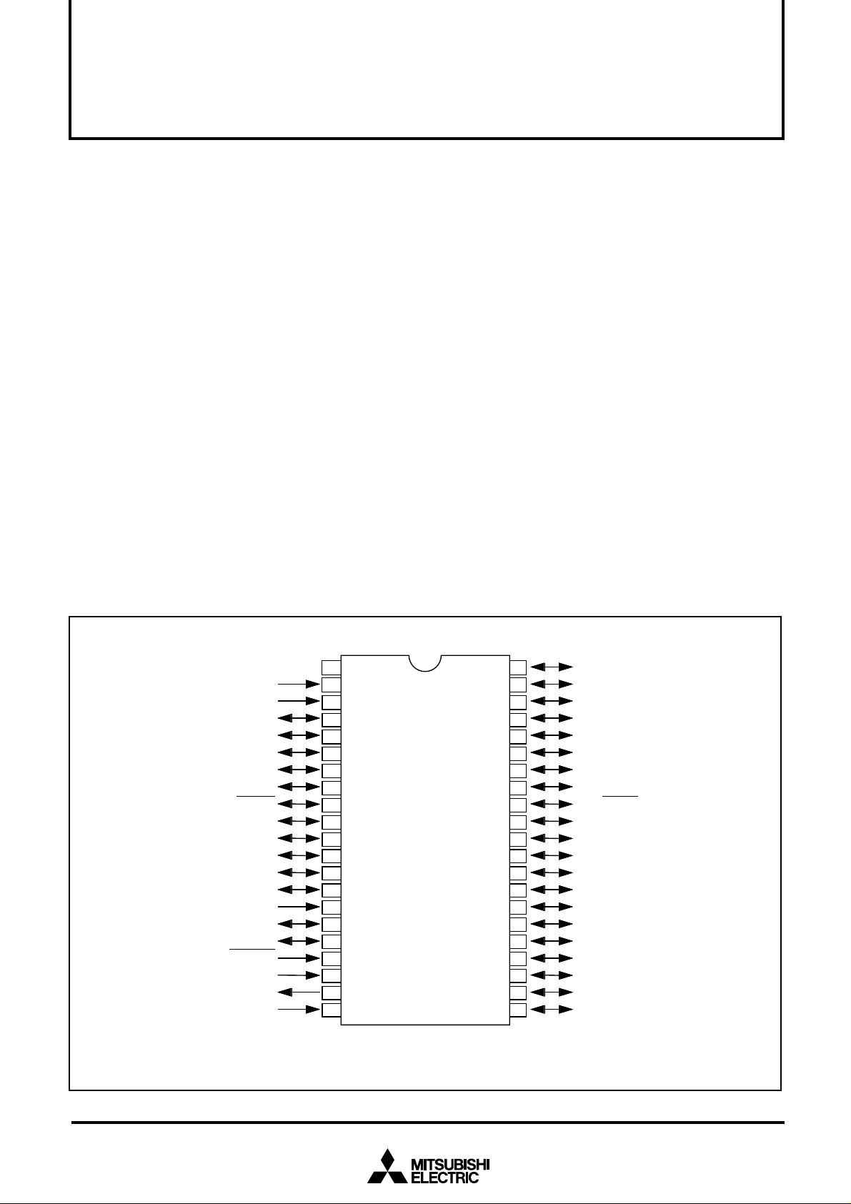
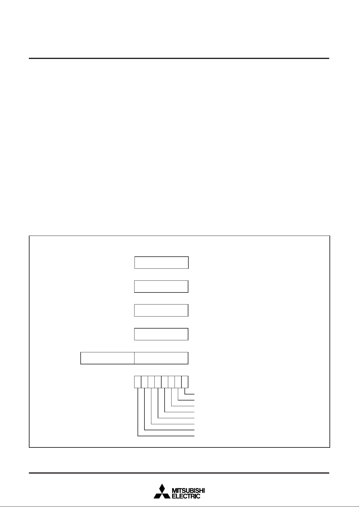
PIN CONFIGURATION (TOP VIEW)
VC
C
R E F
V
S
S
V
A
P 44/ I N T3/ P W M
M P
P 43/ I N T2/ SC
P 42/ I N T1
P 41/ I N T0
P 40/ C N T R1
C N T
D Y
7/
P 2
R0/ SR
L
P 26/ SC
P 25/ T x
P 24/ R x
I
P 21/ XC
O U
P 20/ XC
Package type : FP ........................... 42P2R-A/E (42-pin plastic-molded SSOP)
Package type : SP ........................... 42P4B (42-pin plastic-molded SDIP)
P 2
P 22
C N VS
R E S E
XI
U
XO
VS
2
1
N
1 0
1 1
1 2
1 3
1 4
1 5
1 6
1 7
1 8
1 9
2 0
2 1
1
2
3
4
5
6
7
8
9
M
P
M
P
3 8 5 0 3 M 4 H - X X X F
3 8 5 0 3 M 4 H - X X X S
4 2
4 1
4 0
3 9
3 8
3 7
3 6
3 5
3 4
3 3
3 2
3 1
3 0
2 9
2 8
2 7
2 6
2 5
2 4
2 3
2 2
P 30/ A N0
P 31/ A N1
P 32/ A N2
P 33/ A N3
P 34/ A N4
N
P 00/ SI
U T
P 01/ SO
L K
P 02/ SC
D Y
P 03/ SR
2
2
P 04
P 05
P 06
P 07
P 10/ ( L E D0)
P 11/ ( L E D1)
P 12/ ( L E D2)
P 13/ ( L E D3)
P 14/ ( L E D4)
P 15/ ( L E D5)
P 16/ ( L E D6)
P 17/ ( L E D7)
2
2
Fig. 1 M38503M4H-XXXFP/SP pin configuration
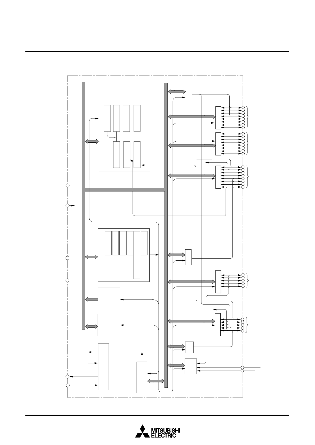
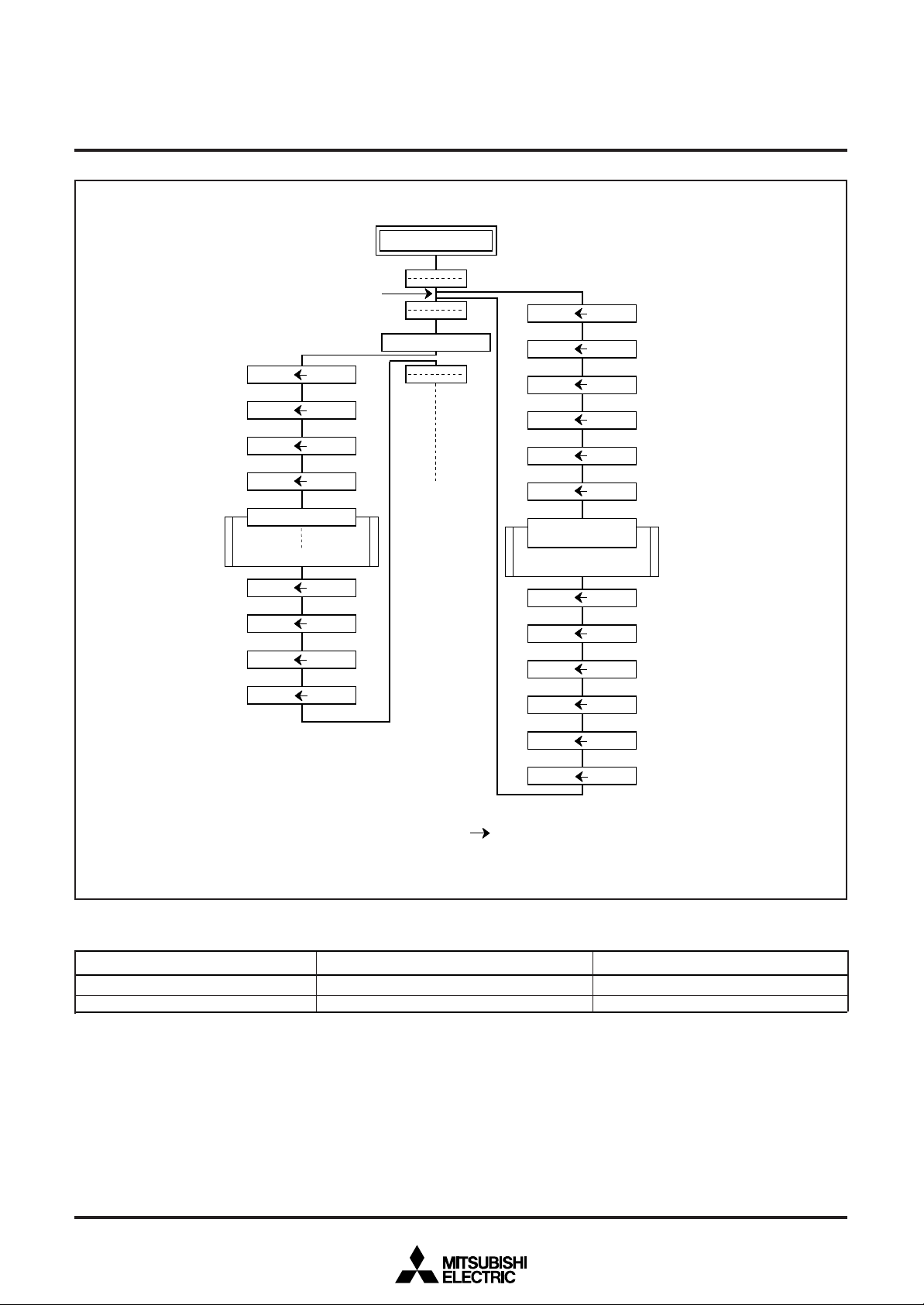
FUNCTIONAL BLOCK
INT
0
–
V
REF
AV
SS
R A M
R O M
C P U
A
X
Y
S
PC
H
PC
L
PS
VSS
21
RESET
18
VCC
1 15
CNV
SS
23
X
IN
19
20
SI/O1(8)
Reset input
Clock generating circuit
Main-clock
input
Main-clock
output
A-D
converter
(10)
CNTR
0
CNTR
1
Timer Y( 8 )
Timer X( 8 )
Prescaler 12(8)
Prescaler X(8)
Prescaler Y(8)
Timer 1( 8 )
Timer 2( 8 )
Sub-clock
input
X
OUT
XCIN
XCOUT
Sub-clock
output
Watchdog
timer
Reset
P2(8)
P3(5)
I/O port P2
I/O port P3
P4(5)
I/O port P4
INT
3
4
6
8
5
7
39
4138 40
42
9
11
13
17
10
12
14
16
P1(8)
I/O port P1
22 24 26 2823
25
27 29
P0(8)
I/O port P0
30 31
32 333435 36
37
PWM
(8)
X
CIN
X
COUT
SI/O2(8)
MITSUBISHI MICROCOMPUTERS
3850 Group (Spec. H)
SINGLE-CHIP 8-BIT CMOS MICROCOMPUTER
FUNCTIONAL BLOCK DIAGRAM
Fig. 2 Functional block diagram
2
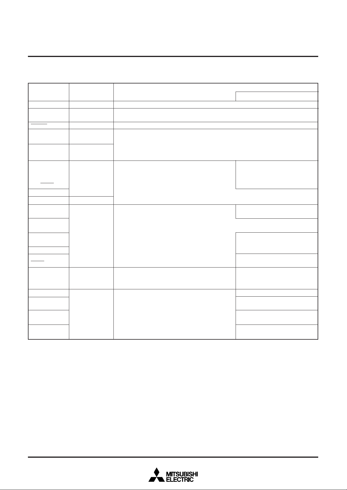
PIN DESCRIPTION
Table 1 Pin description
MITSUBISHI MICROCOMPUTERS
3850 Group (Spec. H)
SINGLE-CHIP 8-BIT CMOS MICROCOMPUTER
VCC, VSS
RESET
XIN
XOUT
P00/SIN2
P01/SOUT2
P02/SCLK2
P03/SRDY2
P04–P07
P20/XCOUT
P21/XCIN
P22
P23
P24/RxD
P25/TxD
P26/SCLK
P27/CNTR0/
SRDY1
P30/AN0–
P34/AN4
P40/CNTR1
P41/INT0
P42/INT1
P43/INT2/SCMP2
P44/INT3/PWM
NamePin
Power source
CNVSS inputCNVSS
Reset input
Clock input
Clock output
I/O port P0
I/O port P1P10–P17
I/O port P2
I/O port P3
I/O port P4
Functions
•Apply voltage of 2.7 V – 5.5 V to Vcc, and 0 V to Vss.
•This pin controls the operation mode of the chip.
•Normally connected to VSS.
•Reset input pin for active “L.”
•Input and output pins for the clock generating circuit.
•Connect a ceramic resonator or quartz-crystal oscillator between the XIN and XOUT pins to set
the oscillation frequency.
•When an external clock is used, connect the clock source to the XIN pin and leave the XOUT
pin open.
•8-bit CMOS I/O port.
•I/O direction register allows each pin to be individually
programmed as either input or output.
•CMOS compatible input level.
•CMOS 3-state output structure.
•P10 to P17 (8 bits) are enabled to output large current for LED drive.
•8-bit CMOS I/O port.
•I/O direction register allows each pin to be individually
programmed as either input or output.
•CMOS compatible input level.
•P20, P21, P24 to P27: CMOS3-state output structure.
•P22, P23: N-channel open-drain structure.
•8-bit CMOS I/O port with the same function as port P0.
•CMOS compatible input level.
•CMOS 3-state output structure.
•8-bit CMOS I/O port with the same function as port P0.
•CMOS compatible input level.
•CMOS 3-state output structure.
Function except a port function
• Serial I/O2 function pin
• Sub-clock generating circuit I/O
pins (connect a resonator)
• Serial I/O1 function pin
• Serial I/O1 function pin/
Timer X function pin
• A-D converter input pin
• Timer Y function pin
• Interrupt input pins
• Interrupt input pin
• SCMP2 output pin
• Interrupt input pin
• PWM output pin
3
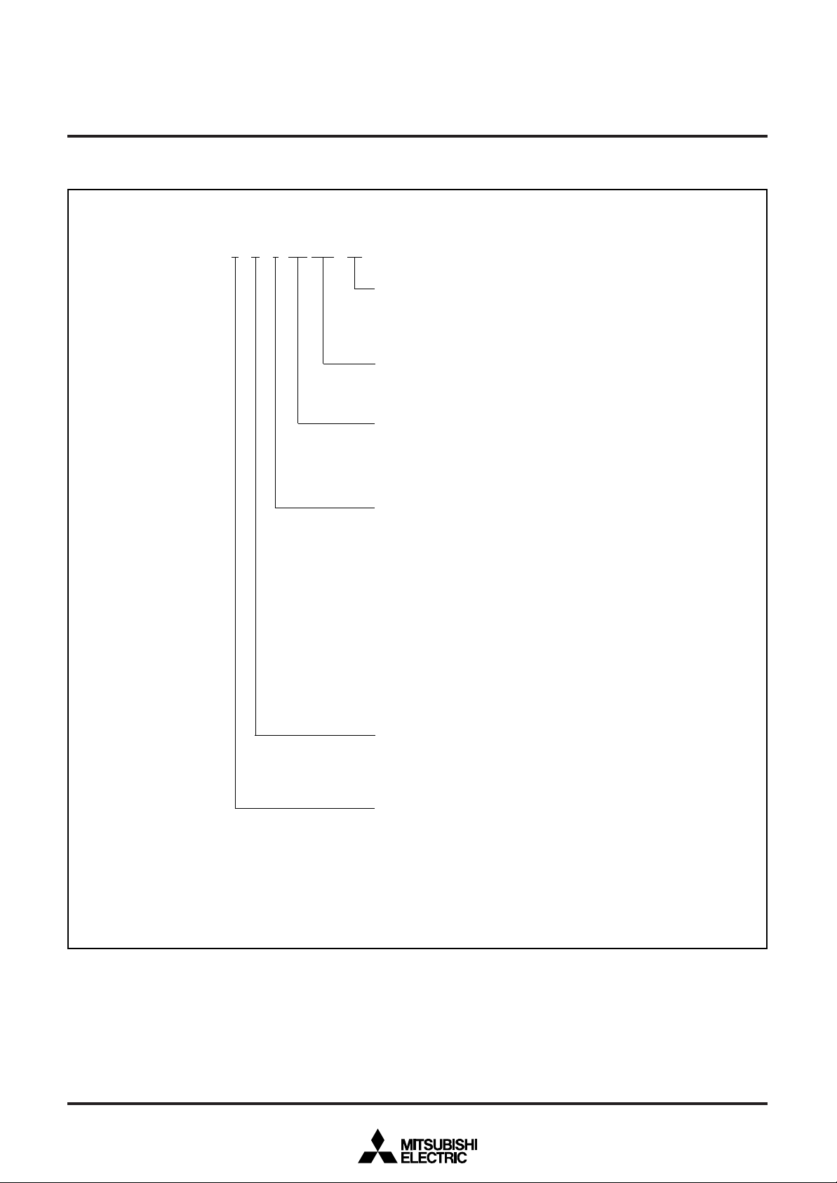
PART NUMBERING
MITSUBISHI MICROCOMPUTERS
3850 Group (Spec. H)
SINGLE-CHIP 8-BIT CMOS MICROCOMPUTER
P r o d u c t n a m e
M 3 8 5 0 3 M 4 H– X X XS P
P a c k a g e t y p e
S P : 4 2 P 4 B
F P : 4 2 P 2 R - A / E
S S : 4 2 S 1 B - A
R O M n u m b e r
O m i t t e d i n O n e T i m e P R O M v e r s i o n s h i p p e d i n b l a n k ,
E P R O M v e r s i o n , a n d f l a s h m e m o r y v e r s i o n .
– : s t a n d a r d
O m i t t e d i n O n e T i m e P R O M v e r s i o n s h i p p e d i n b l a n k , E P R O M
v e r s i o n , a n d f l a s h m e m o r y v e r s i o n .
H – : P a r t i a l s p e c i f i c a t i o n c h a n g e d v e r s i o n
R O M / P R O M / F l a s h m e m o r y s i z e
: 3 6 8 6 4 b y t e s
: 4 0 9 6 b y t e s
1
: 8 1 9 2 b y t e s
2
: 1 2 2 8 8 b y t e s
3
: 1 6 3 8 4 b y t e s
4
: 2 0 4 8 0 b y t e s
5
: 2 4 5 7 6 b y t e s
6
: 2 8 6 7 2 b y t e s
7
: 3 2 7 6 8 b y t e s
8
T h e f i r s t 1 2 8 b y t e s a n d t h e l a s t 2 b y t e s o f R O M a r e r e s e r v e d a r e a s ; t h e y
c a n n o t b e u s e d a s a u s e r ’ s R O M a r e a .
H o w e v e r , t h e y c a n b e p r o g r a m m e d o r e r a s e d i n t h e f l a s h m e m o r y v e r s i o n ,
s o t h a t t h e u s e r s c a n u s e t h e m .
9
: 4 0 9 6 0 b y t e s
A
: 4 5 0 5 6 b y t e s
B
: 4 9 1 5 2 b y t e s
C
: 5 3 2 4 8 b y t e s
D
: 5 7 3 4 4 b y t e s
E
: 6 1 4 4 0 b y t e s
F
Fig. 3 Part numbering
M e m o r y t y p e
M: M a s k R O M v e r s i o n
E : E P R O M o r O n e T i m e P R O M v e r s i o n
F: F l a s h m e m o r y v e r s i o n
R A M s i z e
5
0
: 1 9 2 b y t e s
1
: 2 5 6 b y t e s
2
: 3 8 4 b y t e s
3
: 5 1 2 b y t e s
4
: 6 4 0 b y t e s
: 7 6 8 b y t e s
6
: 8 9 6 b y t e s
7
: 1 0 2 4 b y t e s
8
: 1 5 3 6 b y t e s
9
: 2 0 4 8 b y t e s
4
MITSUBISHI MICROCOMPUTERS
3850 Group (Spec. H)
SINGLE-CHIP 8-BIT CMOS MICROCOMPUTER
GROUP EXPANSION
Mitsubishi plans to expand the 3850 group (spec. H) as follows.
Memory Type
Support for mask ROM, One Time PROM, and flash memory versions.
Memory Size
Flash memory size .........................................................32 K bytes
One Time PROM size.....................................................24 K bytes
Mask ROM size ................................................... 8 K to 32 K bytes
RAM size ...............................................................512 to 1 K bytes
Memory Expansion Plan
R O M s i z e ( b y t e s )
R O M
e x t e r a n a l
3 2 K
2 8 K
M a s s p r o d u c t i o n
U n d e r d e v e l o p m e n t
Packages
42P4B ......................................... 42-pin shrink plastic-molded DIP
42P2R-A/E........................................... 42-pin plastic-molded SOP
42S1B-A .................. 42-pin shrink ceramic DIP (EPROM version)
A s o f F e b . 2 0 0 0
M 3 8 5 0 7 M 8 / F 8
2 4 K
2 0 K
M a s s p r o d u c t i o n
1 6 K
1 2 K
M a s s p r o d u c t i o n
8 K
3 8 45 1 26 4 07 6 88 9 61 0 2 4
P r o d u c t s u n d e r d e v e l o p m e n t o r p l a n n i n g : t h e d e v e l o p m e n t s c h e d u l e a n d s p e c i f i c a t i o n m a y b e r e v i s e d w i t h o u t n o t i c e .
T h e d e v e l o p m e n t o f pl a n n i n g p r o d u c t s m a y b e s t o p p e d .
Fig. 4 Memory expansion plan
M 3 8 5 0 4 M 6 / E 6
M 3 8 5 0 3 M 4 H
M 3 8 5 0 3 M 2 H
1 1 5 21 2 8 01 4 0 81 5 3 62 0 4 8
R A M s i z e ( b y t e s )
5
Currently planning products are listed below.
MITSUBISHI MICROCOMPUTERS
3850 Group (Spec. H)
SINGLE-CHIP 8-BIT CMOS MICROCOMPUTER
Table 2 Support products
Product name
M38503M2H-XXXSP
M38503M2H-XXXFP
M38503M4H-XXXSP
M38503M4H-XXXFP
M38504M6-XXXSP
M38504E6-XXXSP
M388504E6SP
M388504E6SS
M38504M6-XXXFP
M38504E6-XXXFP
M38504E6FP
Table 3 3850 group (standard) and 3850 group (spec. H)
corresponding products
3850 group (standard)
M38503M2-XXXFP/SP
M38503M4-XXXFP/SP
M38503E4-XXXFP/SP
M38503E4FP/SP
M38503E4SS
ROM size (bytes)
ROM size for User in ( )
8192
(8062)
16384
(16254)
24576
(24446)
3850 group (spec. H)
M38503M2H-XXXFP/SP
M38503M4H-XXXFP/SP
M38504M6-XXXFP/SP
M38504E6-XXXFP/SP
M38504E6FP/SP
M38504E6SS
M38507M8-XXXFP/SP
M38507F8FP/SP
RAM size (bytes)
512
512
640
Package
42P4B
42P2R-A/E
424P4B
42P2R-A/E
424P4B
42S1B-A
42P2R-A/E
As of Feb. 2000
Remarks
Mask ROM version
Mask ROM version
Mask ROM version
Mask ROM version
Mask ROM version
One Time PROM version
One Time PROM version (blank)
EPROM version
Mask ROM version
One Time PROM version
One Time PROM version (blank)
Table 4 Differences between 3850 group (standard) and 3850 group (spec. H)
3850 group (spec. H)
Serial I/O
A-D converter
Large current port
3850 group (standard)
1: Serial I/O (UART or Clock-synchronized)
Unserviceable in low-speed mode
5: P13–P17
2: Serial I/O1 (UART or Clock-synchronized)
Serial I/O2 (Clock-synchronized)
Serviceable in low-speed mode
8: P10–P17
Notes on differences between 3850 group (standard) and 3850 group (spec. H)
(1) The absolute maximum ratings of 3850 group (spec. H) is smaller than that of 3850 group (standard).
•Power source voltage Vcc = –0.3 to 6.5 V
•CNVss input voltage VI = –0.3 to Vcc +0.3 V
(2) The oscillation circuit constants of XIN-XOUT, XCIN-XCOUT may be some differences between 3850 group (standard) and 3850 group
(spec. H).
(3) Do not write any data to the reserved area and the reserved bit. (Do not change the contents after rest.)
(4) Fix bit 3 of the CPU mode register to “1”.
(5) Be sure to perform the termination of unused pins.
6
MITSUBISHI MICROCOMPUTERS
3850 Group (Spec. H)
SINGLE-CHIP 8-BIT CMOS MICROCOMPUTER
FUNCTIONAL DESCRIPTION
CENTRAL PROCESSING UNIT (CPU)
The 3850 group (spec. H) uses the standard 740 Family instruction set. Refer to the table of 740 Family addressing modes and
machine instructions or the 740 Family Software Manual for details on the instruction set.
Machine-resident 740 Family instructions are as follows:
The FST and SLW instructions cannot be used.
The STP, WIT, MUL, and DIV instructions can be used.
[Accumulator (A)]
The accumulator is an 8-bit register. Data operations such as data
transfer, etc., are executed mainly through the accumulator.
[Index Register X (X)]
The index register X is an 8-bit register. In the index addressing
modes, the value of the OPERAND is added to the contents of
register X and specifies the real address.
[Index Register Y (Y)]
The index register Y is an 8-bit register. In partial instruction, the
value of the OPERAND is added to the contents of register Y and
specifies the real address.
[Stack Pointer (S)]
The stack pointer is an 8-bit register used during subroutine calls
and interrupts. This register indicates start address of stored area
(stack) for storing registers during subroutine calls and interrupts.
The low-order 8 bits of the stack address are determined by the
contents of the stack pointer. The high-order 8 bits of the stack address are determined by the stack page selection bit. If the stack
page selection bit is “0” , the high-order 8 bits becomes “0016”. If
the stack page selection bit is “1”, the high-order 8 bits becomes
“0116”.
The operations of pushing register contents onto the stack and
popping them from the stack are shown in Figure 6.
Store registers other than those described in Figure 6 with program when the user needs them during interrupts or subroutine
calls.
[Program Counter (PC)]
The program counter is a 16-bit counter consisting of two 8-bit
registers PCH and PCL. It is used to indicate the address of the
next instruction to be executed.
b7
b0
A Accumulator
b7
b0
X Index register X
b7
b0
Y Index register Y
b7 b0
S Stack pointer
b7b15 b0
H
PC
L
Program counterPC
b7 b0
N V T B D I Z C Processor status register (PS)
Carry flag
Zero flag
Interrupt disable flag
Decimal mode flag
Break flag
Index X mode flag
Overflow flag
Negative flag
Fig. 5 740 Family CPU register structure
7
e
O n - g o i n g R o u t i n
MITSUBISHI MICROCOMPUTERS
3850 Group (Spec. H)
SINGLE-CHIP 8-BIT CMOS MICROCOMPUTER
P u s h r e t u r n a d d r e s s
o n s t a c k
P O P re t u r n
a d d r e s s f r o m s t a c k
I n t e r r u p t r e q u e s t
M ( S )( P CH)
( S )
M ( S )( P CL)
( S )
S u b r o u t i n e
E x e c u t e R T S
( S )
( P CL)M ( S )
( S )
( P CH)M ( S )
( S ) – 1
( S ) + 1
( S ) + 1
( N o t e )
( S ) – 1
E x e c u t e J S R
M ( S )( P CH)
( S )
( S ) – 1
M ( S )( P CL)
( S )
( S ) – 1
M ( S )( P S )
( S )
( S ) – 1
I n t e r r u p t
S e r v i c e R o u t i n e
E x e c u t e R T I
( S )
( S ) + 1
( P S )M ( S )
( S )
( S ) + 1
( P CL)M ( S )
( S )
( S ) + 1
P u s h r e t u r n a d d r e s s
o n s t a c k
P u s h c o n t e n t s o f p r o c e s s o r
s t a t u s r e g i s t e r o n s t a c k
I F l a g i s s e t f r o m “ 0 ” t o “ 1 ”
F e t c h t h e j u m p v e c t o r
P O P c o n t e n t s o f
p r o c e s s o r s t a t u s
r e g i s t e r f r o m s t a c k
P O P r e t u r n
a d d r e s s
f r o m s t a c k
N o t e: C o n d i t i o n f o r a c c e p t a n c e o f a n i n t e r r u p t I n t e r r u p t e n a b l e f l a g i s “ 1 ”
Fig. 6 Register push and pop at interrupt generation and subroutine call
Table 5 Push and pop instructions of accumulator or processor status register
Push instruction to stack
Accumulator
Processor status register
PHA
PHP
I n t e r r u p t d i s a b l e f l a g i s “ 0 ”
( P CH)M ( S )
Pop instruction from stack
PLA
PLP
8
MITSUBISHI MICROCOMPUTERS
3850 Group (Spec. H)
SINGLE-CHIP 8-BIT CMOS MICROCOMPUTER
[Processor status register (PS)]
The processor status register is an 8-bit register consisting of 5
flags which indicate the status of the processor after an arithmetic
operation and 3 flags which decide MCU operation. Branch operations can be performed by testing the Carry (C) flag , Zero (Z) flag,
Overflow (V) flag, or the Negative (N) flag. In decimal mode, the Z,
V, N flags are not valid.
•Bit 0: Carry flag (C)
The C flag contains a carry or borrow generated by the arithmetic
logic unit (ALU) immediately after an arithmetic operation. It can
also be changed by a shift or rotate instruction.
•Bit 1: Zero flag (Z)
The Z flag is set if the result of an immediate arithmetic operation
or a data transfer is “0”, and cleared if the result is anything other
than “0”.
•Bit 2: Interrupt disable flag (I)
The I flag disables all interrupts except for the interrupt
generated by the BRK instruction.
Interrupts are disabled when the I flag is “1”.
•Bit 3: Decimal mode flag (D)
The D flag determines whether additions and subtractions are
executed in binary or decimal. Binary arithmetic is executed when
this flag is “0”; decimal arithmetic is executed when it is “1”.
Decimal correction is automatic in decimal mode. Only the ADC
and SBC instructions can be used for decimal arithmetic.
•Bit 4: Break flag (B)
The B flag is used to indicate that the current interrupt was
generated by the BRK instruction. The BRK flag in the processor
status register is always “0”. When the BRK instruction is used to
generate an interrupt, the processor status register is pushed
onto the stack with the break flag set to “1”.
•Bit 5: Index X mode flag (T)
When the T flag is “0”, arithmetic operations are performed
between accumulator and memory. When the T flag is “1”, direct
arithmetic operations and direct data transfers are enabled
between memory locations.
•Bit 6: Overflow flag (V)
The V flag is used during the addition or subtraction of one byte
of signed data. It is set if the result exceeds +127 to -128. When
the BIT instruction is executed, bit 6 of the memory location
operated on by the BIT instruction is stored in the overflow flag.
•Bit 7: Negative flag (N)
The N flag is set if the result of an arithmetic operation or data
transfer is negative. When the BIT instruction is executed, bit 7 of
the memory location operated on by the BIT instruction is stored
in the negative flag.
Table 6 Set and clear instructions of each bit of processor status register
C flag Z flag I flag D flag B flag T flag V flag N flag
Set instruction
Clear instruction
SEC
CLC
_
_
SEI
CLI
SED
CLD
_
_
SET
CLT CLV
_
_
_
9
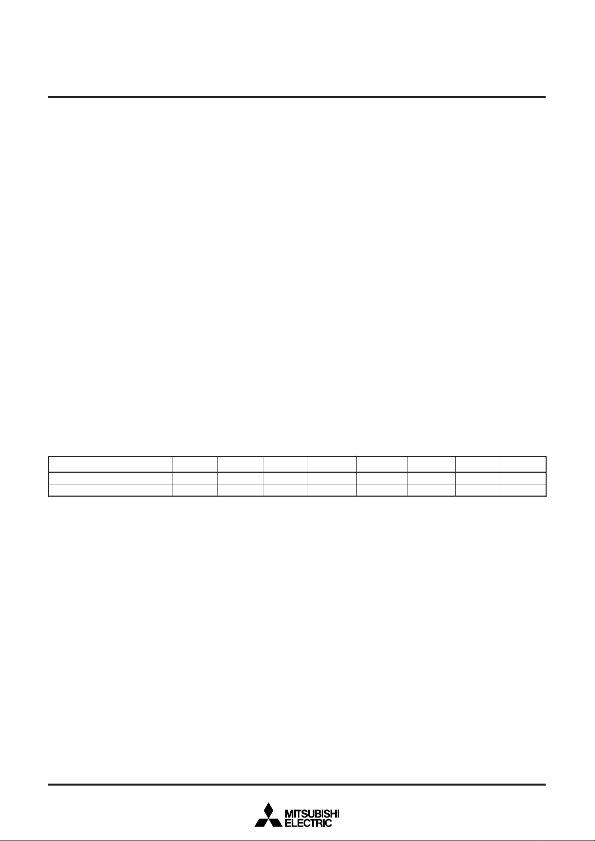
[CPU Mode Register (CPUM)] 003B16
The CPU mode register contains the stack page selection bit, etc.
The CPU mode register is allocated at address 003B16.
MITSUBISHI MICROCOMPUTERS
3850 Group (Spec. H)
SINGLE-CHIP 8-BIT CMOS MICROCOMPUTER
b7
b0
CPU mode register
(
CPUM : address
003B16)
Processor mode bits
b1 b0
0 0 : Single-chip mode
0 1 :
1 0 : Not available
1 1 :
Stack page selection bit
0 : 0 page
1 : 1 page
Fix this bit to “1”.
C switch bit
Port X
0 : I/O port function (stop oscillating)
CIN–XCOUT oscillating function
1 : X
Main clock (X
0 : Oscillating
1 : Stopped
Main clock division ratio selection bits
b7 b6
0 0 : φ = f(X
0 1 : φ = f(X
1 0 : φ = f(X
1 1 : Not available
IN–XOUT) stop bit
IN)/2 (high-speed mode)
IN)/8 (middle-speed mode)
CIN)/2 (low-speed mode)
Fig. 7 Structure of CPU mode register
10
MITSUBISHI MICROCOMPUTERS
3850 Group (Spec. H)
SINGLE-CHIP 8-BIT CMOS MICROCOMPUTER
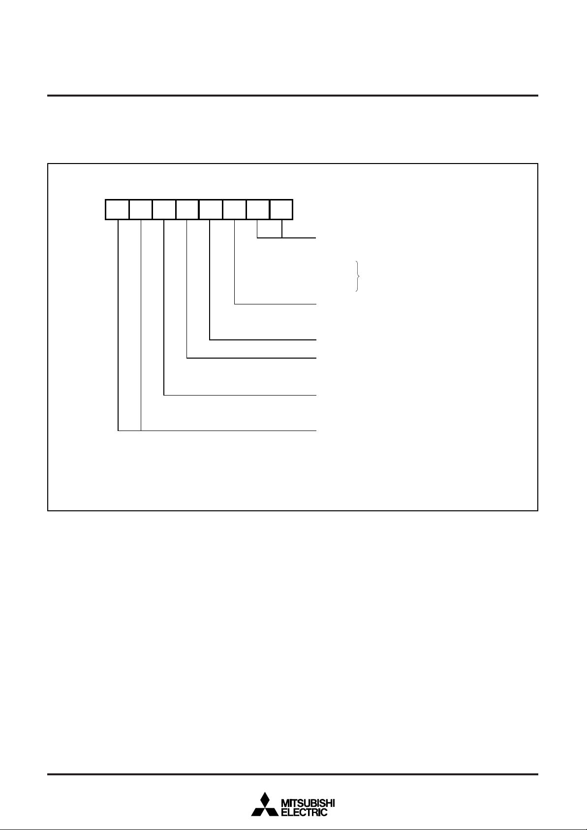
MEMORY
Special Function Register (SFR) Area
The Special Function Register area in the zero page contains
control registers such as I/O ports and timers.
RAM
RAM is used for data storage and for stack area of subroutine
calls and interrupts.
ROM
The first 128 bytes and the last 2 bytes of ROM are reserved for
device testing and the rest is user area for storing programs.
Interrupt Vector Area
The interrupt vector area contains reset and interrupt vectors.
RAM area
RAM size
(bytes)
192
256
384
512
640
768
896
1024
1536
2048
ROM area
ROM size
(bytes)
4096
8192
12288
16384
20480
24576
28672
32768
36864
40960
45056
49152
53248
57344
61440
Address
XXXX
00FF
013F
01BF
023F
02BF
033F
03BF
043F
063F
083F
Address
YYYY
F000
E000
D000
C000
B000
A000
9000
8000
7000
6000
5000
4000
3000
2000
1000
16
16
16
16
16
16
16
16
16
16
16
Address
16
16
16
16
16
16
16
16
16
16
16
16
16
16
16
16
ZZZZ
F080
E080
D080
C080
B080
A080
9080
8080
7080
6080
5080
4080
3080
2080
1080
16
16
16
16
16
16
16
16
16
16
16
16
16
16
16
16
Zero Page
Access to this area with only 2 bytes is possible in the zero page
addressing mode.
Special Page
Access to this area with only 2 bytes is possible in the special
page addressing mode.
0000
16
0040
16
0100
16
XXXX
0FF0
0FFF
YYYY
ZZZZ
16
16
16
16
16
RAM
ROM
FF00
16
FFDC
16
FFFE
16
FFFF
16
Note: Flash memory version only
SFR area
Not used
SFR area (Note)
Not used
Reserved ROM area
(128 bytes)
Interrupt vector area
Reserved ROM area
Zero page
Special page
Fig. 8 Memory map diagram
11
MITSUBISHI MICROCOMPUTERS
3850 Group (Spec. H)
SINGLE-CHIP 8-BIT CMOS MICROCOMPUTER
0 0 0 0
0 0 0 1
0 0 0 2
0 0 0 3
0 0 0 4
0 0 0 5
0 0 0 6
0 0 0 7
0 0 0 8
0 0 0 9
0 0 0 A
0 0 0 B
0 0 0 C
0 0 0 D
0 0 0 E
0 0 0 F
0 0 1 0
0 0 1 1
0 0 1 2
0 0 1 3
0 0 1 4
0 0 1 5
0 0 1 6
0 0 1 7
0 0 1 8
0 0 1 9
0 0 1 A
0 0 1 B
0 0 1 C
0 0 1 D
0 0 1 E
0 0 1 F
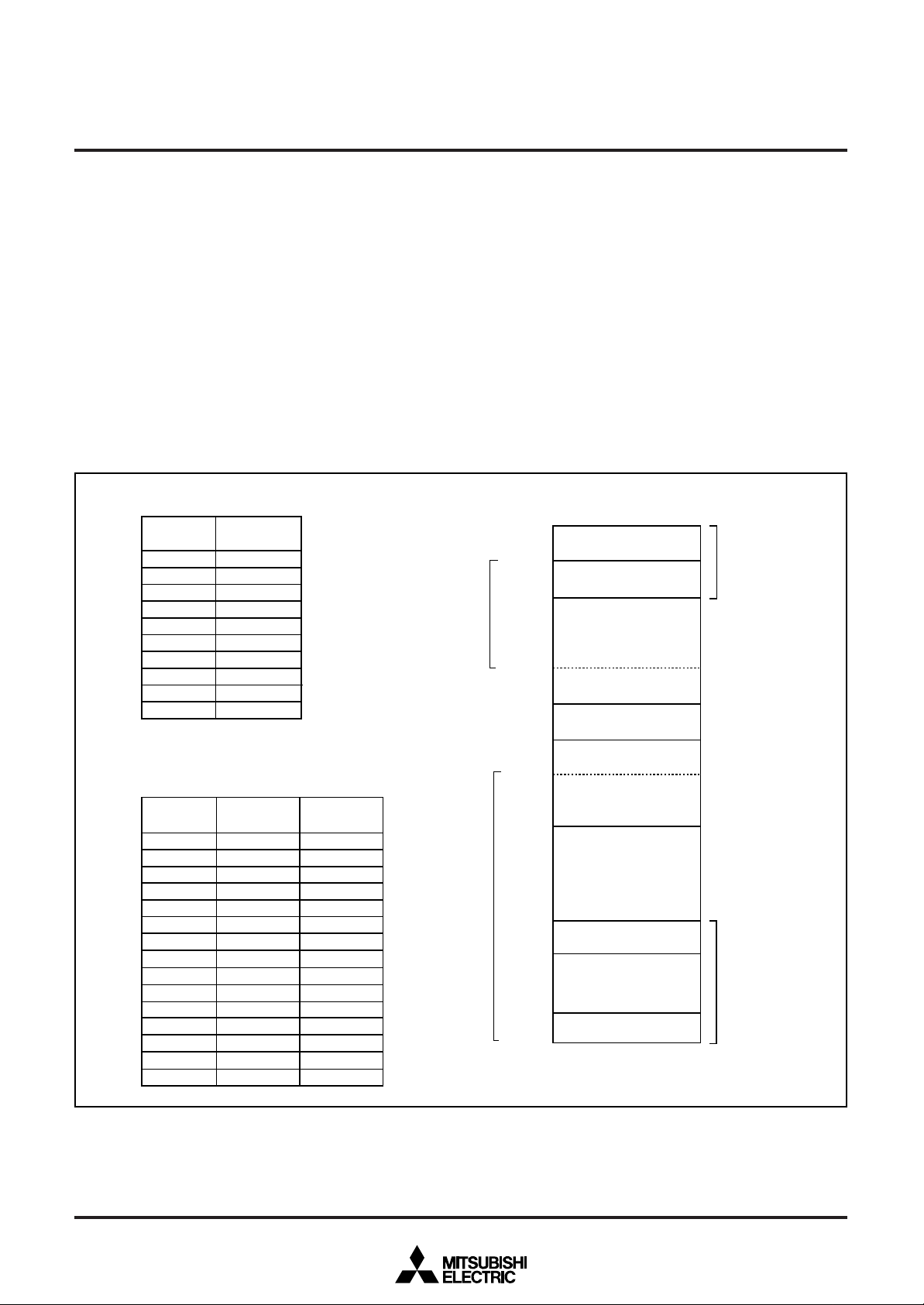
P o r t P 0 ( P 0 )
1 6
P o r t P 0 d i r e c t i o n r e g i s t e r ( P 0 D )
1 6
P o r t P 1 ( P 1 )
1 6
P o r t P 1 d i r e c t i o n r e g i s t e r ( P 1 D )
1 6
P o r t P 2 ( P 2 )
1 6
P o r t P 2 d i r e c t i o n r e g i s t e r ( P 2 D )
1 6
P o r t P 3 ( P 3 )
1 6
P o r t P 3 d i r e c t i o n r e g i s t e r ( P 3 D )
1 6
P o r t P 4 ( P 4 )
1 6
P o r t P 4 d i r e c t i o n r e g i s t e r ( P 4 D )
1 6
1 6
1 6
1 6
1 6
1 6
1 6
1 6
1 6
1 6
R e s e r v e d ✽
1 6
R e s e r v e d ✽
1 6
R e s e r v e d ✽
S e r i a l I / O 2 c o n t r o l r e g i s t e r 1 ( S I O 2 C O N 1 )
1 6
S e r i a l I / O 2 c o n t r o l r e g i s t e r 2 ( S I O 2 C O N 2 )
1 6
S e r i a l I / O 2 r e g i s t e r ( S I O 2 )
1 6
T r a n s m i t / R e c e i v e b u f f e r r e g i s t e r ( T B / R B )
1 6
S e r i a l I / O 1 s t a t u s r e g i s t e r ( S I O S T S )
1 6
S e r i a l I / O 1 c o n t r o l r e g i s t e r ( S I O C O N )
1 6
U A R T c o n t r o l r e g i s t e r ( U A R T C O N )
1 6
B a u d r a t e g e n e r a t o r ( B R G )
1 6
P W M c o n t r o l r e g i s t e r ( P W M C O N )
1 6
P W M p r e s c a l e r ( P R E P W M )
1 6
P W M r e g i s t e r ( P W M )
1 6
0 0 2 0
0 0 2 1
0 0 2 2
0 0 2 3
0 0 2 4
0 0 2 5
0 0 2 6
0 0 2 7
0 0 2 8
0 0 2 9
0 0 2 A
0 0 2 B
0 0 2 C
0 0 2 D
0 0 2 E
0 0 2 F
0 0 3 0
0 0 3 1
0 0 3 2
0 0 3 3
0 0 3 4
0 0 3 5
0 0 3 6
0 0 3 7
0 0 3 8
0 0 3 9
0 0 3 A
0 0 3 B
0 0 3 C
0 0 3 D
0 0 3 E
0 0 3 F
P r e s c a l e r 1 2 ( P R E 1 2 )
1 6
T i m e r 1 ( T 1 )
1 6
T i m e r 2 ( T 2 )
1 6
T i m e r X Y m o d e r e g i s t e r ( T M )
1 6
P r e s c a l e r X ( P R E X )
1 6
T i m e r X ( T X )
1 6
P r e s c a l e r Y ( P R E Y )
1 6
T i m e r Y ( T Y )
1 6
T i m e r c o u n t s o u r c e s e l e c t i o n r e g i s t e r ( T C S S )
1 6
1 6
1 6
1 6
R e s e r v e d ✽
R e s e r v e d ✽
1 6
1 6
R e s e r v e d ✽
1 6
R e s e r v e d ✽
1 6
R e s e r v e d ✽
1 6
R e s e r v e d ✽
1 6
R e s e r v e d ✽
1 6
1 6
A - D c o n t r o l r e g i s t e r ( A D C O N )
1 6
A - D c o n v e r s i o n l o w - o r d e r r e g i s t e r ( A D L )
1 6
A - D c o n v e r s i o n h i g h - o r d e r r e g i s t e r ( A D H )
1 6
1 6
R e s e r v e d ✽
M I S R G
1 6
W a t c h d o g t i m e r c o n t r o l r e g i s t e r ( W D T C O N )
1 6
I n t e r r u p t e d g e s e l e c t i o n r e g i s t e r ( I N T E D G E )
1 6
C P U m o d e r e g i s t e r ( C P U M )
1 6
I n t e r r u p t r e q u e s t r e g i s t e r 1 ( I R E Q 1 )
1 6
I n t e r r u p t r e q u e s t r e g i s t e r 2 ( I R E Q 2 )
1 6
I n t e r r u p t c o n t r o l r e g i s t e r 1 ( I C O N 1 )
1 6
I n t e r r u p t c o n t r o l r e g i s t e r 2 ( I C O N 2 )
1 6
✽ R e s e r v e d : D o n o t w r i t e a n y d a t a t o t h i s a d d r e s s e s , b e c a u s e t h e s e a r e a s a r e r e s e r v e d .
Fig. 9 Memory map of special function register (SFR)
12
I/O PORTS
The I/O ports have direction registers which determine the input/
output direction of each individual pin. Each bit in a direction
register corresponds to one pin, and each pin can be set to be
input port or output port.
When “0” is written to the bit corresponding to a pin, that pin
becomes an input pin. When “1” is written to that bit, that pin
becomes an output pin.
If data is read from a pin which is set to output, the value of the
port output latch is read, not the value of the pin itself. Pins set to
input are floating. If a pin set to input is written to, only the port
output latch is written to and the pin remains floating.
Table 5 I/O port function
Pin
P00/SIN2
P01/SOUT2
P02/SCLK2
P03/SRDY2
P04–P07
P10–P17
P20/XCOUT
P21/XCIN
P22
P23
P24/RxD
P25/TxD
Name
Port P0
Port P1
Port P2
Input/Output
Input/output,
individual
bits
I/O Structure Non-Port Function
CMOS compatible
input level
CMOS 3-state output
CMOS compatible
input level
N-channel open-drain
output
MITSUBISHI MICROCOMPUTERS
3850 Group (Spec. H)
SINGLE-CHIP 8-BIT CMOS MICROCOMPUTER
Related SFRs
Serial I/O2 function I/O
Sub-clock generating
circuit
Serial I/O1 function I/O
Serial I/O2 control
register
CPU mode register
Serial I/O1 control
register
Ref.No.
(1)
(2)
(3)
(4)
(5)
(6)
(7)
(8)
(9)
(10)
P26/SCLK
P27/CNTR0/SRDY1
P30/AN0–
P34/AN4
P40/CNTR1
P41/INT0
P42/INT1
P43/INT2/SCMP2
P44/INT3/PWM
Port P3
Port P4
CMOS compatible
input level
CMOS 3-state output
Serial I/O1 function I/O
Serial I/O1 function I/O
Timer X function I/O
A-D conversion input
Timer Y function I/O
External interrupt input
External interrupt input
SCMP2 output
External interrupt input
PWM output
Serial I/O1 control
register
Serial I/O1 control
register
Timer XY mode register
A-D control register
Timer XY mode register
Interrupt edge selection
register
Interrupt edge selection
register
Serial I/O2 control register
Interrupt edge selection
register
PWM control register
(11)
(12)
(13)
(14)
(15)
(16)
(17)
13
MITSUBISHI MICROCOMPUTERS
r
t
3850 Group (Spec. H)
SINGLE-CHIP 8-BIT CMOS MICROCOMPUTER
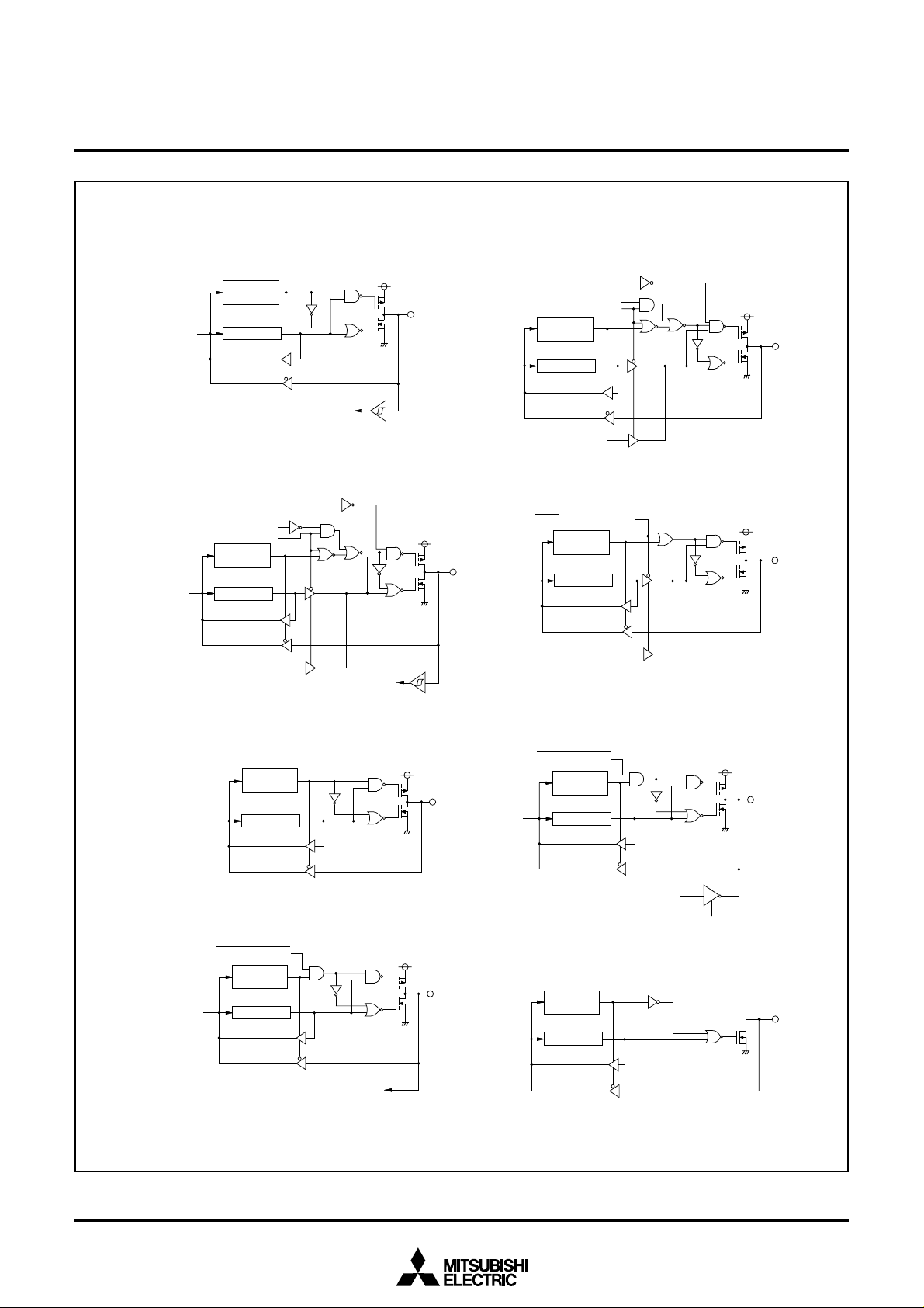
( 1 ) P o r t P 0
( 3 ) P o r t P 0
0
D a t a b u s
2
P 02/ S
C L K 2
S e r i a l I / O 2 s y n c h r o n o u s
S e r i a l I / O 2 p o r t s e l e c t i o n b i t
D a t a b u s
S e r i a l I / O 2 c l o c k o u t p u t
D i r e c t i o n
r e g i s t e r
P o r t l a t c h
S e r i a l I / O 2 i n p u t
P - c h a n n e l o u t p u t d i s a b l e b i t
c l o c k s e l e c t i o n b i t
D i r e c t i o n
r e g i s t e r
P o r t l a t c h
S e r i a l I / O 2 e x t e r n a l c l o c k i n p u t
( 2 ) P o r t P 0
P 01/ S
S e r i a l I / O 2 T r a n s m i t c o m p l e t i o n s i g n a l
D a t a b u s
( 4 ) P o r t P 0
1
O U T 2
P - c h a n n e l o u t p u t d i s a b l e b i t
S e r i a l I / O 2 p o r t s e l e c t i o n b i t
D i r e c t i o n
r e g i s t e r
P o r t l a t c h
S e r i a l I / O 2 o u t p u t
3
R D Y 2
o u t p u t e n a b l e b i t
S
D i r e c t i o n
r e g i s t e r
D a t a b u s
P o r t l a t c h
S e r i a l I / O 2 r e a d y o u t p u t
( 5 ) P o r t s P 04- P 0
( 7 ) P o r t P 2
D a t a b u s
D a t a b u s
1
7 ,
P o r t X
P 1
C
D i r e c t i o n
r e g i s t e r
P o r t l a t c h
Fig. 10 Port block diagram (1)
D i r e c t i o n
r e g i s t e r
P o r t l a t c h
s w i t c h b i t
S u b - c l o c k g e n e r a t i n g c i r c u i t i n p u
( 6 ) P o r t P 2
D a t a b u s
( 8 ) P o r t s P 2
D a t a b u s
0
C
s w i t c h b i t
P o r t X
D i r e c t i o n
r e g i s t e r
P o r t l a t c h
O s c i l l a t o
P o r t P 2
1
P o r t XC s w i t c h b i t
2 ,
P 2
3
D i r e c t i o n
r e g i s t e r
P o r t l a t c h
14
MITSUBISHI MICROCOMPUTERS
3850 Group (Spec. H)
SINGLE-CHIP 8-BIT CMOS MICROCOMPUTER
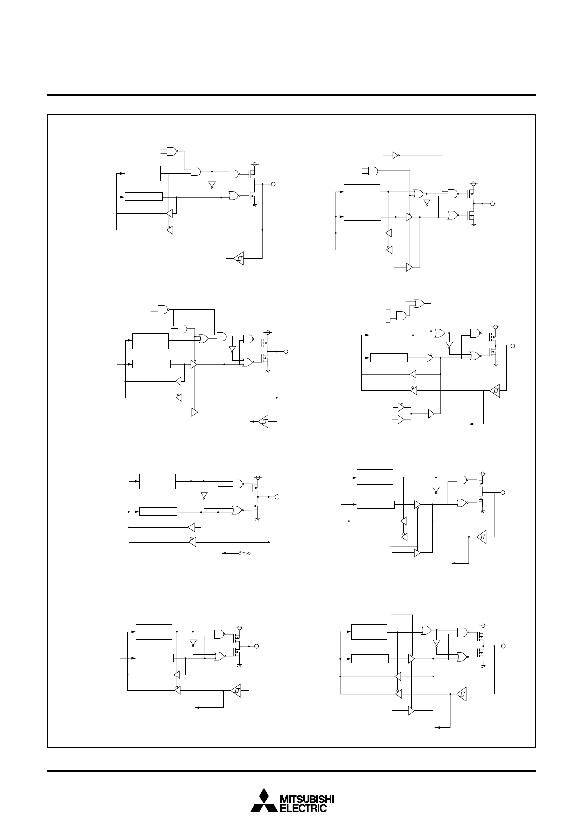
(9) Port P24
Serial I/O1 enable bit
Receive enable bit
Data bus
(11) Port P26
Serial I/O1 synchronous
clock selection bit
Serial I/O1 enable bit
Serial I/O1 mode selection bit
Serial I/O1 enable bit
Data bus
Serial I/O1 clock output
Direction
register
Port latch
Direction
register
Port latch
Serial I/O1 input
External clock input
(10) Port P25
P-channel output disable bit
Serial I/O1 enable bit
Transmit enable bit
Direction
register
Data bus
Port latch
Serial I/O1 output
(12) Port P27
Serial I/O1 mode selection bit
S
Pulse output mode
Serial I/O1 enable bit
RDY1 output enable bit
Data bus
Serial ready output
Timer output
Direction
register
Port latch
Pulse output mode
CNTR
0 interrupt
input
(13) Ports P30-P34
Data bus
(15) Ports P41,P42
Data bus
Direction
register
Port latch
Direction
register
Port latch
Interrupt input
A-D converter input
Analog input pin selection bit
(14) Port P40
Data bus
Pulse output mode
(16) Port P43
comparison signal control bit
Data bus
comparison signal output
Direction
register
Port latch
Timer output
Serial I/O2 I/O
Direction
register
Port latch
Serial I/O2 I/O
CNTR
1 interrupt
Interrupt input
input
Fig. 11 Port block diagram (2)
15
MITSUBISHI MICROCOMPUTERS
3850 Group (Spec. H)
SINGLE-CHIP 8-BIT CMOS MICROCOMPUTER
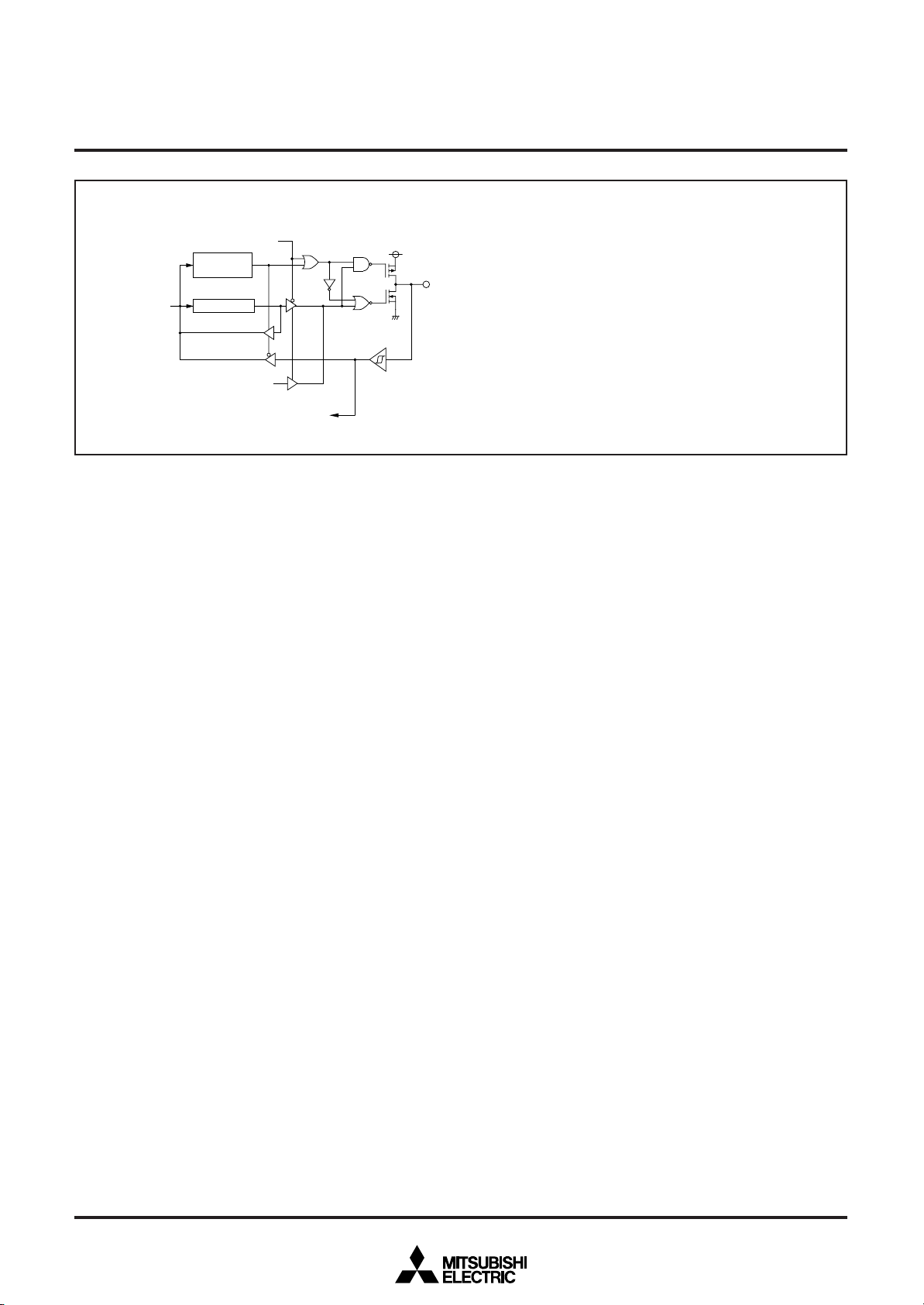
(17) Port P4
Data bus
4
PWM output enable bit
Direction
register
Port latch
PWM output
Fig. 12 Port block diagram (3)
Interrupt input
16

MITSUBISHI MICROCOMPUTERS
3850 Group (Spec. H)
SINGLE-CHIP 8-BIT CMOS MICROCOMPUTER
INTERRUPTS
Interrupts occur by 14 sources among 14 sources: six external,
seven internal, and one software.
Interrupt Control
Each interrupt is controlled by an interrupt request bit, an interrupt
enable bit, and the interrupt disable flag except for the software interrupt set by the BRK instruction. An interrupt occurs if the
corresponding interrupt request and enable bits are “1” and the interrupt disable flag is “0”.
Interrupt enable bits can be set or cleared by software.
Interrupt request bits can be cleared by software, but cannot be
set by software.
The BRK instruction cannot be disabled with any flag or bit. The I
(interrupt disable) flag disables all interrupts except the BRK instruction interrupt.
When several interrupts occur at the same time, the interrupts are
received according to priority.
Interrupt Operation
By acceptance of an interrupt, the following operations are automatically performed:
1. The contents of the program counter and the processor status
register are automatically pushed onto the stack.
2. The interrupt disable flag is set and the corresponding interrupt
request bit is cleared.
3. The interrupt jump destination address is read from the vector
table into the program counter.
■Notes
When the active edge of an external interrupt (INT0–INT3, CNTR0,
CNTR1) is set, the corresponding interrupt request bit may also be
set. Therefore, take the following sequence:
1. Disable the interrupt
2. Change the interrupt edge selection register
(the timer XY mode register for CNTR0 and CNTR1)
3. Clear the interrupt request bit to “0”
4. Accept the interrupt.
17

Table 8 Interrupt vector addresses and priority
Interrupt Source
Reset (Note 2)
INT0
Reserved
INT1
INT2
INT3/ Serial I/O2
Reserved
Timer X
Timer Y
Timer 1
Timer 2
Serial I/O1
reception
Serial I/O1
transmission
CNTR0
CNTR1
A-D converter
BRK instruction
Notes 1: Vector addresses contain interrupt jump destination addresses.
2: Reset function in the same way as an interrupt with the highest priority.
Priority
1
2
3
4
5
6
7
8
9
10
11
12
13
14
15
16
17
Vector Addresses (Note 1)
High
FFFD16
FFFB16
FFF916
FFF716
FFF516
FFF316
FFF116
FFEF16
FFED16
FFEB16
FFE916
FFE716
FFE516
FFE316
FFE116
FFDF16
Low
FFFC16
FFFA16
FFF816
FFF616
FFF416
FFF216
FFF016
FFEE16
FFEC16
FFEA16
FFE816
FFE616
FFE416
FFE216
FFE016
FFDE16
FFDC16FFDD16
MITSUBISHI MICROCOMPUTERS
3850 Group (Spec. H)
SINGLE-CHIP 8-BIT CMOS MICROCOMPUTER
Interrupt Request
Generating Conditions
At reset
At detection of either rising or
falling edge of INT0 input
Reserved
At detection of either rising or
falling edge of INT1 input
At detection of either rising or
falling edge of INT2 input
At detection of either rising or
falling edge of INT3 input/ At
completion of serial I/O2 data
reception/transmission
Reserved
At timer X underflow
At timer Y underflow
At timer 1 underflow
At timer 2 underflow
At completion of serial I/O1 data
reception
At completion of serial I/O1
transfer shift or when transmission buffer is empty
At detection of either rising or
falling edge of CNTR0 input
At detection of either rising or
falling edge of CNTR1 input
At completion of A-D conversion
At BRK instruction execution
Remarks
Non-maskable
External interrupt
(active edge selectable)
External interrupt
(active edge selectable)
External interrupt
(active edge selectable)
External interrupt
(active edge selectable)
Switch by Serial I/O2/INT3
interrupt source bit
STP release timer underflow
Valid when serial I/O1 is selected
Valid when serial I/O1 is selected
External interrupt
(active edge selectable)
External interrupt
(active edge selectable)
Non-maskable software interrupt
18

Interrupt request bit
Interrupt enable bit
Interrupt disable flag (I)
MITSUBISHI MICROCOMPUTERS
3850 Group (Spec. H)
SINGLE-CHIP 8-BIT CMOS MICROCOMPUTER
BRK instruction
Reset
Fig. 13 Interrupt control
b 7 b 0
I n t e r r u p t e d g e s e l e c t i o n r e g i s t e r
1 6
( I N T E D G E : a d d r e s s 0 0 3 A
)
I N T0 a c t i v e e d g e s e l e c t i o n b i t
1
a c t i v e e d g e s e l e c t i o n b i t
I N T
2
a c t i v e e d g e s e l e c t i o n b i t
I N T
3
a c t i v e e d g e s e l e c t i o n b i t
I N T
S e r i a l I / O 2 / I N T
0 : I N T
3
3
i n t e r r u p t s o u r c e b i t
i n t e r r u p t s e l e c t e d
0 : F a l l i n g e d g e a c t i v e
1 : R i s i n g e d g e a c t i v e
1 : S e r i a l I / O 2 i n t e r r u p t s e l e c t e d
N o t u s e d ( r e t u r n s “ 0 ” w h e n r e a d )
b 7 b 0 b 7 b 0
I n t e r r u p t r e q u e s t r e g i s t e r 1
( I R E Q 1 : a d d r e s s 0 0 3 C
1 6
)
I N T0 i n t e r r u p t r e q u e s t b i t
R e s e r v e d
1
i n t e r r u p t r e q u e s t b i t
I N T
2
i n t e r r u p t r e q u e s t b i t
I N T
3
/ S e r i a l I / O 2 i n t e r r u p t r e q u e s t b i t
I N T
R e s e r v e d
T i m e r X i n t e r r u p t r e q u e s t b i t
T i m e r Y i n t e r r u p t r e q u e s t b i t
0 : N o i n t e r r u p t r e q u e s t i s s u e d
1 : I n t e r r u p t r e q u e s t i s s u e d
Interrupt request
I n t e r r u p t r e q u e s t r e g i s t e r 2
1 6
( I R E Q 2 : a d d r e s s 0 0 3 D
)
T i m e r 1 i n t e r r u p t r e q u e s t b i t
T i m e r 2 i n t e r r u p t r e q u e s t b i t
S e r i a l I / O 1 r e c e p t i o n i n t e r r u p t r e q u e s t b i t
S e r i a l I / O 1 t r a n s m i t i n t e r r u p t r e q u e s t b i t
0
i n t e r r u p t r e q u e s t b i t
C N T R
C N T R
1
i n t e r r u p t r e q u e s t b i t
A D c o n v e r t e r i n t e r r u p t r e q u e s t b i t
N o t u s e d ( r e t u r n s “ 0 ” w h e n r e a d )
0 : N o i n t e r r u p t r e q u e s t i s s u e d
1 : I n t e r r u p t r e q u e s t i s s u e d
b 7 b 0 b 7 b 0
I n t e r r u p t c o n t r o l r e g i s t e r 1
( I C O N 1 : a d d r e s s 0 0 3 E
1 6
)
I N T0 i n t e r r u p t e n a b l e b i t
R e s e r v e d ( D o n o t w r i t e “ 1 ” t o t h i s b i t . )
1
i n t e r r u p t e n a b l e b i t
I N T
2
i n t e r r u p t e n a b l e b i t
I N T
3
/ S e r i a l I / O 2 i n t e r r u p t e n a b l e b i t
I N T
R e s e r v e d ( D o n o t w r i t e “ 1 ” t o t h i s b i t . )
T i m e r X i n t e r r u p t e n a b l e b i t
T i m e r Y i n t e r r u p t e n a b l e b i t
0 : I n t e r r u p t s d i s a b l e d
1 : I n t e r r u p t s e n a b l e d
Fig. 14 Structure of interrupt-related registers
I n t e r r u p t c o n t r o l r e g i s t e r 2
1 6
( I C O N 2 : a d d r e s s 0 0 3 F
)
T i m e r 1 i n t e r r u p t e n a b l e b i t
T i m e r 2 i n t e r r u p t e n a b l e b i t
S e r i a l I / O 1 r e c e p t i o n i n t e r r u p t e n a b l e b i t
S e r i a l I / O 1 t r a n s m i t i n t e r r u p t e n a b l e b i t
0
i n t e r r u p t e n a b l e b i t
C N T R
1
i n t e r r u p t e n a b l e b i t
C N T R
A D c o n v e r t e r i n t e r r u p t e n a b l e b i t
N o t u s e d ( r e t u r n s “ 0 ” w h e n r e a d )
( D o n o t w r i t e “ 1 ” t o t h i s b i t . )
0 : I n t e r r u p t s d i s a b l e d
1 : I n t e r r u p t s e n a b l e d
19

MITSUBISHI MICROCOMPUTERS
3850 Group (Spec. H)
SINGLE-CHIP 8-BIT CMOS MICROCOMPUTER
TIMERS
The 3850 group (spec. H) has four timers: timer X, timer Y, timer
1, and timer 2.
The division ratio of each timer or prescaler is given by 1/(n + 1),
where n is the value in the corresponding timer or prescaler latch.
All timers are count down. When the timer reaches “0016”, an underflow occurs at the next count pulse and the corresponding
timer latch is reloaded into the timer and the count is continued.
When a timer underflows, the interrupt request bit corresponding
to that timer is set to “1”.
b7
Fig. 15 Structure of timer XY mode register
b0
Timer XY mode register
(TM : address 0023
Timer X operating mode bit
b1b0
0 0: Timer mode
0 1: Pulse output mode
1 0: Event counter mode
1 1: Pulse width measurement mode
CNTR0 active edge selection bit
0: Interrupt at falling edge
Count at rising edge in event
counter mode
1: Interrupt at rising edge
Count at falling edge in event
counter mode
Timer X count stop bit
0: Count start
1: Count stop
Timer Y operating mode bits
b5b4
0 0: Timer mode
0 1: Pulse output mode
1 0: Event counter mode
1 1: Pulse width measurement mode
CNTR
1
active edge selection bit
0: Interrupt at falling edge
Count at rising edge in event
counter mode
1: Interrupt at rising edge
Count at falling edge in event
counter mode
Timer Y count stop bit
0: Count start
1: Count stop
16
)
Timer 1 and Timer 2
The count source of prescaler 12 is the oscillation frequency
which is selected by timer 12 count source selection bit. The output of prescaler 12 is counted by timer 1 and timer 2, and a timer
underflow sets the interrupt request bit.
Timer X and Timer Y
Timer X and Timer Y can each select in one of four operating
modes by setting the timer XY mode register.
(1) Timer Mode
The timer counts the count source selected by Timer count source
selection bit.
(2) Pulse Output Mode
The timer counts the count source selected by Timer count source
selection bit. Whenever the contents of the timer reach “0016”, the
signal output from the CNTR0 (or CNTR1) pin is inverted. If the
CNTR0 (or CNTR1) active edge selection bit is “0”, output begins
at “ H”.
If it is “1”, output starts at “L”. When using a timer in this mode, set
the corresponding port P27 ( or port P40) direction register to output mode.
(3) Event Counter Mode
Operation in event counter mode is the same as in timer mode,
except that the timer counts signals input through the CNTR0 or
CNTR1 pin.
When the CNTR0 (or CNTR1) active edge selection bit is “0”, the
rising edge of the CNTR0 (or CNTR1) pin is counted.
When the CNTR0 (or CNTR1) active edge selection bit is “1”, the
falling edge of the CNTR0 (or CNTR1) pin is counted.
(4) Pulse Width Measurement Mode
If the CNTR0 (or CNTR1) active edge selection bit is “0”, the timer
counts the selected signals by the count source selection bit while
the CNTR0 (or CNTR1) pin is at “H”. If the CNTR0 (or CNTR1) active edge selection bit is “1”, the timer counts it while the CNTR0
(or CNTR1) pin is at “L”.
b7
b0
Timer count source selection register
(TCSS : address 0028
Timer X count source selection bit
IN)/16 (f(XCIN)/16 at low-speed mode)
0 : f(X
1 : f(XIN)/2 (f(XCIN)/2 at low-speed mode)
Timer Y count source selection bit
0 : f(X
IN)/16 (f(XCIN)/16 at low-speed mode)
1 : f(XIN)/2 (f(XCIN)/2 at low-speed mode)
Timer 12 count source selection bit
IN)/16 (f(XCIN)/16 at low-speed mode)
0 : f(X
1 : f(XCIN)
Not used (returns “0” when read)
16)
Fig. 16 Structure of timer count source selection register
20
The count can be stopped by setting “1” to the timer X (or timer Y)
count stop bit in any mode. The corresponding interrupt request
bit is set each time a timer underflows.
■Note
When switching the count source by the timer 12, X and Y count
source bit, the value of timer count is altered in unconsiderable
amount owing to generating of a thin pulses in the count input
signals.
Therefore, select the timer count source before set the value to
the prescaler and the timer.

Data bus
MITSUBISHI MICROCOMPUTERS
3850 Group (Spec. H)
SINGLE-CHIP 8-BIT CMOS MICROCOMPUTER
(f(X
CIN
)/16 at low-speed mode)
CIN
)/2 at low-speed mode)
(f(X
P2
7
/CNTR
direction register
CIN
)/16 at low-speed mode)
(f(X
CIN
)/2 at low-speed mode)
(f(X
P40/CNTR
direction register
f(XIN)/16
f(XIN)/2
Timer X count source selection bit
CNTR
0
active
0
edge selection
“0”
bit
“1”
Port P2
7
Port P2
latch
Pulse output mode
f(XIN)/16
f(XIN)/2
Timer Y count source selection bit
1
active
CNTR
1
edge selection
bit
“0”
“1”
Port P4
Port P4
0
latch
Pulse output mode
Pulse width
measurement
mode
7
0
Event
counter
mode
CNTR
edge selection
bit
Pulse width
measurement mode
Event
counter
mode
CNTR
edge selection
bit
Timer mode
Pulse output mode
Timer X count stop bit
0
active
“1”
“0”
Timer mode
Pulse output mode
Timer Y count stop bit
1
active
“1”
“0”
Data bus
Prescaler X latch (8)
Prescaler X (8)
Q
Toggle flip-flop
Q
R
Data bus
Prescaler Y latch (8)
Prescaler Y (8)
Q
Toggle flip-flop
Q
R
Timer X latch (8)
Timer X (8)
To timer X interrupt
request bit
0
interrupt
To CNTR
request bit
T
Timer X latch write pulse
Pulse output mode
Timer Y latch (8)
Timer Y (8)
To timer Y interrupt
request bit
1
interrupt
To CNTR
request bit
T
Timer Y latch write pulse
Pulse output mode
Prescaler 12 latch (8)
CIN
)/16 at low-speed mode)
(f(X
f(XIN)/16
f(X
CIN
)
Prescaler 12 (8)
Timer 12 count source selection bit
Fig. 17 Block diagram of timer X, timer Y, timer 1, and timer 2
Timer 1 latch (8)
Timer 1 (8)
Timer 2 latch (8)
Timer 2 (8)
To timer 2 interrupt
request bit
To timer 1 interrupt
request bit
21

MITSUBISHI MICROCOMPUTERS
3850 Group (Spec. H)
SINGLE-CHIP 8-BIT CMOS MICROCOMPUTER
SERIAL I/O1
Serial I/O1 can be used as either clock synchronous or asynchronous (UART) serial I/O. A dedicated timer is also provided for
baud rate generation.
Data bus
Address 0018
Shift clock
Serial I/O1 synchronous
clock selection bit
Frequency division ratio 1/(n+1)
Transmit shift register
Transmit buffer register
Data bus
P24/RXD
P26/S
7/SRDY1
P2
P2
5/TX
X
CLK
BRG count source selection bit
IN
F/F
D
Receive buffer register
Receive shift register
1/4
Falling-edge detector
(1) Clock Synchronous Serial I/O Mode
Clock synchronous serial I/O mode can be selected by setting the
serial I/O1 mode selection bit of the serial I/O1 control register (bit
6 of address 001A16) to “1”.
For clock synchronous serial I/O, the transmitter and the receiver
must use the same clock. If an internal clock is used, transfer is
started by a write signal to the TB/RB.
16
Clock control circuit
Baud rate generator
Address 001C
Shift clock
Address 0018
16
Clock control circuit
16
Serial I/O1 control register
Receive buffer full flag (RBF)
Receive interrupt request (RI)
1/4
Transmit interrupt source selection bit
Serial I/O1 status register
Address 001A
Transmit shift completion flag (TSC)
Transmit interrupt request (TI)
Transmit buffer empty flag (TBE)
Address 0019
16
16
Fig. 18 Block diagram of clock synchronous serial I/O1
Transfer shift clock
(1/2 to 1/2048 of the internal
clock, or an external clock)
Serial output TxD
Serial input RxD
Receive enable signal S
RDY1
D
0
D
0
D
D
Write pulse to receive/transmit
buffer register (address 0018
16
)
TBE = 0
TBE = 1
TSC = 0
1: As the transmit interrupt (TI), either when the transmit buffer has emptied (TBE=1) or after the transmit shift operation has
Notes
ended (TSC=1), by setting the transmit interrupt source selection bit (TIC) of the serial I/O1 control register.
2: If data is written to the transmit buffer register when TSC=0, the transmit clock is generated continuously and serial data
is output continuously from the TxD pin.
3: The receive interrupt (RI) is set when the receive buffer full flag (RBF) becomes “1” .
Fig. 19 Operation of clock synchronous serial I/O1 function
D
1
D
2
1
D
2
D
3
D
3
D
4
D
4
D
5
D
5
D
6
D
6
7
D
7
RBF = 1
TSC = 1
Overrun error (OE)
detection
22

MITSUBISHI MICROCOMPUTERS
r
r
r
K
D
3850 Group (Spec. H)
SINGLE-CHIP 8-BIT CMOS MICROCOMPUTER
(2) Asynchronous Serial I/O (UART) Mode
Clock asynchronous serial I/O mode (UART) can be selected by
clearing the serial I/O1 mode selection bit (b6) of the serial I/O1
control register to “0”.
Eight serial data transfer formats can be selected, and the transfer
formats used by a transmitter and receiver must be identical.
The transmit and receive shift registers each have a buffer, but the
D a t a b u s
A d d r e s s 0 0 1 8
O E
/ RXD
C L
X
/ T
S T d e t e c t o
B R G c o u n t s o u r c e s e l e c t i o n b i t
I N
X
4
P 2
P 2
P 2
6
/ S
5
C h a r a c t e r l e n g t h s e l e c t i o n b i t
7 b i t s
8 b i t s
S e r i a l I / O s y n c h r o n o u s c l o c k s e l e c t i o n b i t
1 / 4
C h a r a c t e r l e n g t h s e l e c t i o n b i t
1 6
R e c e i v e b u f f e r r e g i s t e r
R e c e i v e s h i f t r e g i s t e r
P EF E
S P d e t e c t o r
F r e q u e n c y d i v i s i o n r a t i o 1 / ( n + 1 )
B a u d r a t e g e n e r a t o r
A d d r e s s 0 0 1 C
S T / S P / P A g e n e r a t o r
T r a n s m i t s h i f t r e g i s t e r
T r a n s m i t b u f f e r r e g i s t e
D a t a b u s
two buffers have the same address in memory. Since the shift register cannot be written to or read from directly, transmit data is
written to the transmit buffer register, and receive data is read
from the receive buffer register.
The transmit buffer register can also hold the next data to be
transmitted, and the receive buffer register can hold a character
while the next character is being received.
S e r i a l I / O 1 c o n t r o l r e g i s t e r
R e c e i v e b u f f e r f u l l f l a g ( R B F )
R e c e i v e i n t e r r u p t r e q u e s t ( R I )
C l o c k c o n t r o l c i r c u i t
1 6
1 / 1 6
T r a n s m i t i n t e r r u p t s o u r c e s e l e c t i o n b i t
S e r i a l I / O 1 s t a t u s r e g i s t e r
0 0 1 8
A d d r e s s
1 6
A d d r e s s 0 0 1 A
1 / 1 6
1 6
U A R T c o n t r o l r e g i s t e
A d d r e s s 0 0 1 B
T r a n s m i t s h i f t c o m p l e t i o n f l a g ( T S C )
T r a n s m i t i n t e r r u p t r e q u e s t ( T I )
T r a n s m i t b u f f e r e m p t y f l a g ( T B E )
A d d r e s s
0 0 1 9
1 6
1 6
Fig. 20 Block diagram of UART serial I/O1
23

Transmit or receive clock
MITSUBISHI MICROCOMPUTERS
3850 Group (Spec. H)
SINGLE-CHIP 8-BIT CMOS MICROCOMPUTER
Transmit buffer write
Receive buffer read
signal
TBE=0 TBE=0
TSC=0
TBE=1
Serial output TXD
signal
X
Serial input R
Notes
D
1: Error flag detection occurs at the same time that the RBF flag becomes “1” (at 1st stop bit, during reception).
2: As the transmit interrupt (TI), when either the TBE or TSC flag becomes “1,” can be selected to occur depending on the setting of the transmit
interrupt source selection bit (TIC) of the serial I/O1 control register.
3: The receive interrupt (RI) is set when the RBF flag becomes “1.”
4: After data is written to the transmit buffer when TSC=1, 0.5 to 1.5 cycles of the data shift cycle is necessary until changing to TSC=0.
ST
0
D
1
1 start bit
7 or 8 data bit
1 or 0 parity bit
1 or 2 stop bit (s)
ST
0
D
1
Fig. 21 Operation of UART serial I/O1 function
[Transmit Buffer Register/Receive Buffer
Register (TB/RB)] 0018
The transmit buffer register and the receive buffer register are located at the same address. The transmit buffer is write-only and
the receive buffer is read-only. If a character bit length is 7 bits, the
MSB of data stored in the receive buffer is “0”.
16
[Serial I/O1 Status Register (SIOSTS)] 001916
The read-only serial I/O1 status register consists of seven flags
(bits 0 to 6) which indicate the operating status of the serial I/O1
function and various errors.
Three of the flags (bits 4 to 6) are valid only in UART mode.
The receive buffer full flag (bit 1) is cleared to “0” when the receive
buffer register is read.
If there is an error, it is detected at the same time that data is
transferred from the receive shift register to the receive buffer register, and the receive buffer full flag is set. A write to the serial I/O1
status register clears all the error flags OE, PE, FE, and SE (bit 3
to bit 6, respectively). Writing “0” to the serial I/O1 enable bit SIOE
(bit 7 of the serial I/O1 control register) also clears all the status
flags, including the error flags.
Bits 0 to 6 of the serial I/O1 status register are initialized to “0” at
reset, but if the transmit enable bit (bit 4) of the serial I/O1 control
register has been set to “1”, the transmit shift completion flag (bit
2) and the transmit buffer empty flag (bit 0) become “1”.
TBE=1
STD
SP
RBF=1
STD
SP D
D
0
D
1
Generated at 2nd bit in 2-stop-bit mode
RBF=0
0
D
1
TSC=1
SP
RBF=1
SP
[Serial I/O1 Control Register (SIOCON)] 001A16
The serial I/O1 control register consists of eight control bits for the
serial I/O1 function.
[UART Control Register (UARTCON)] 001B16
The UART control register consists of four control bits (bits 0 to 3)
which are valid when asynchronous serial I/O is selected and set
the data format of an data transfer and one bit (bit 4) which is always valid and sets the output structure of the P25/TXD pin.
[Baud Rate Generator (BRG)] 001C16
The baud rate generator determines the baud rate for serial transfer.
The baud rate generator divides the frequency of the count source
by 1/(n + 1), where n is the value written to the baud rate generator.
24

MITSUBISHI MICROCOMPUTERS
3850 Group (Spec. H)
SINGLE-CHIP 8-BIT CMOS MICROCOMPUTER
b 7
b 0
S e r i a l I / O 1 s t a t u s r e g i s t e r
( S I O S T S : a d d r e s s 0 0 1 9
1 6
)
b 7
T r a n s m i t b u f f e r e m p t y f l a g ( T B E )
0 : B u f f e r f u l l
1 : B u f f e r e m p t y
R e c e i v e b u f f e r f u l l f l a g ( R B F )
0 : B u f f e r e m p t y
1 : B u f f e r f u l l
T r a n s m i t s h i f t c o m p l e t i o n f l a g ( T S C )
0 : T r a n s m i t s h i f t i n p r o g r e s s
1 : T r a n s m i t s h i f t c o m p l e t e d
O v e r r u n e r r o r f l a g ( O E )
0 : N o e r r o r
1 : O v e r r u n e r r o r
P a r i t y e r r o r f l a g ( P E )
0 : N o e r r o r
1 : P a r i t y e r r o r
F r a m i n g e r r o r f l a g ( F E )
0 : N o e r r o r
1 : F r a m i n g e r r o r
S u m m i n g e r r o r f l a g ( S E )
0 : ( O E ) U ( P E ) U ( F E ) = 0
1 : ( O E ) U ( P E ) U ( F E ) = 1
N o t u s e d ( r e t u r n s “ 1 ” w h e n r e a d )
b 0
S e r i a l I / O 1 c o n t r o l r e g i s t e r
( S I O C O N : a d d r e s s 0 0 1 A
1 6
)
B R G c o u n t s o u r c e s e l e c t i o n b i t ( C S S )
I N
)
0 : f ( X
I N
) / 4
1 : f ( X
S e r i a l I / O 1 s y n c h r o n o u s c l o c k s e l e c t i o n b i t ( S C S )
0 : B R G o u t p u t d i v i d e d b y 4 w h e n c l o c k s y n c h r o n o u s
s e r i a l I / O 1 i s s e l e c t e d , B R G o u t p u t d i v i d e d b y 1 6
w h e n U A R T i s s e l e c t e d .
1 : E x t e r n a l c l o c k i n p u t w h e n c l o c k s y n c h r o n o u s s e r i a l
I / O 1 i s s e l e c t e d , e x t e r n a l c l o c k i n p u t d i v i d e d b y 1 6
w h e n U A R T i s s e l e c t e d .
R D Y 1
o u t p u t e n a b l e b i t ( S R D Y )
S
7
p i n o p e r a t e s a s o r d i n a r y I / O p i n
0 : P 2
7
p i n o p e r a t e s a s S
1 : P 2
R D Y 1
o u t p u t p i n
T r a n s m i t i n t e r r u p t s o u r c e s e l e c t i o n b i t ( T I C )
0 : I n t e r r u p t w h e n t r a n s m i t b u f f e r h a s e m p t i e d
1 : I n t e r r u p t w h e n t r a n s m i t s h i f t o p e r a t i o n i s c o m p l e t e d
T r a n s m i t e n a b l e b i t ( T E )
0 : T r a n s m i t d i s a b l e d
1 : T r a n s m i t e n a b l e d
R e c e i v e e n a b l e b i t ( R E )
0 : R e c e i v e d i s a b l e d
1 : R e c e i v e e n a b l e d
S e r i a l I / O 1 m o d e s e l e c t i o n b i t ( S I O M )
0 : C l o c k a s y n c h r o n o u s ( U A R T ) s e r i a l I / O
1 : C l o c k s y n c h r o n o u s s e r i a l I / O
S e r i a l I / O 1 e n a b l e b i t ( S I O E )
b 7
b 0
U A R T c o n t r o l r e g i s t e r
( U A R T C O N : a d d r e s s 0 0 1 B
1 6
)
C h a r a c t e r l e n g t h s e l e c t i o n b i t ( C H A S )
0 : S e r i a l I / O 1 d i s a b l e d
4
( p i n s P 2
t o P 27 o p e r a t e a s o r d i n a r y I / O p i n s )
1 : S e r i a l I / O 1 e n a b l e d
4
( p i n s P 2
t o P 27 o p e r a t e a s s e r i a l I / O 1 p i n s )
0 : 8 b i t s
1 : 7 b i t s
P a r i t y e n a b l e b i t ( P A R E )
0 : P a r i t y c h e c k i n g d i s a b l e d
1 : P a r i t y c h e c k i n g e n a b l e d
P a r i t y s e l e c t i o n b i t ( P A R S )
0 : E v e n p a r i t y
1 : O d d p a r i t y
S t o p b i t l e n g t h s e l e c t i o n b i t ( S T P S )
0 : 1 s t o p b i t
1 : 2 s t o p b i t s
5
/ TXD P - c h a n n e l o u t p u t d i s a b l e b i t ( P O F F )
P 2
0 : C M O S o u t p u t ( i n o u t p u t m o d e )
1 : N - c h a n n e l o p e n d r a i n o u t p u t ( i n o u t p u t m o d e )
N o t u s e d ( r e t u r n “ 1 ” w h e n r e a d )
Fig. 22 Structure of serial I/O1 control registers
25

SERIAL I/O2
The serial I/O2 can be operated only as the clock synchronous type.
As a synchronous clock for serial transfer, either internal clock or
external clock can be selected by the serial I/O2 synchronous clock
selection bit (b6) of serial I/O2 control register 1.
The internal clock incorporates a dedicated divider and permits selecting 6 types of clock by the internal synchronous clock selection
bits (b2, b1, b0) of serial I/O2 control register 1.
Regarding SOUT2 and SCLK2 being output pins, either CMOS output
format or N-channel open-drain output format can be selected by the
P01/SOUT2, P02/SCLK2 P-channel output disable bit (b7) of
serial I/O2 control register 1.
When the internal clock has been selected, a transfer starts by a
write signal to the serial I/O2 register (address 001716). After completion of data transfer, the level of the SOUT2 pin goes to high impedance automatically but bit 7 of the serial I/O2 control register 2 is not
set to “1” automatically.
When the external clock has been selected, the contents of the serial
I/O2 register is continuously sifted while transfer clocks are input.
Accordingly, control the clock externally. Note that the SOUT2 pin does
not go to high impedance after completion of data transfer.
To cause the SOUT2 pin to go to high impedance in the case where
the external clock is selected, set bit 7 of the serial I/O2 control register 2 to “1” when SCLK2 is “H” after completion of data transfer. After
the next data transfer is started (the transfer clock falls), bit 7 of the
serial I/O2 control register 2 is set to “0” and the SOUT2 pin is put into
the active state.
Regardless of the internal clock to external clock, the interrupt request bit is set after the number of bits (1 to 8 bits) selected by the
optional transfer bit is transferred. In case of a fractional number of
bits less than 8 bits as the last data, the received data to be stored in
the serial I/O2 register becomes a fractional number of bits close to
MSB if the transfer direction selection bit of serial I/O2 control register 1 is LSB first, or a fractional number of bits close to LSB if the said
bit is MSB first. For the remaining bits, the previously received data
is shifted.
At transmit operation using the clock synchronous serial I/O, the SCMP2
signal can be output by comparing the state of the transmit pin SOUT2
with the state of the receive pin SIN2 in synchronization with a rise of
the transfer clock. If the output level of the SOUT2 pin is equal to the
input level to the SIN2 pin, “L” is output from the SCMP2 pin. If not, “H”
is output. At this time, an INT2 interrupt request can also be generated. Select a valid edge by bit 2 of the interrupt edge selection register (address 003A16).
MITSUBISHI MICROCOMPUTERS
3850 Group (Spec. H)
SINGLE-CHIP 8-BIT CMOS MICROCOMPUTER
b 7
b 7 b 0
Fig. 23 Structure of Serial I/O2 control registers 1, 2
b 0
S e r i a l I / O 2 c o n t r o l r e g i s t e r 1
( S I O 2 C O N 1 : a d d r e s s 0 0 1 5
I n t e r n a l s y n c h r o n o u s c l o c k s e l e c t i o n b i t s
b 2 b 1 b 0
0 0 0 : f ( X
0 0 1 : f ( X
0 1 0 : f ( X
0 1 1 : f ( X
1 1 0 : f ( X
1 1 1 : f ( X
S e r i a l I / O 2 p o r t s e l e c t i o n b i t
0 : I / O p o r t
1 : S
S
0 : P 0
1 : P 0
T r a n s f e r d i r e c t i o n s e l e c t i o n b i t
0 : L S B f i r s t
1 : M S B f i r s t
S e r i a l I / O 2 s y n c h r o n o u s c l o c k s e l e c t i o n b i t
0 : E x t e r n a l c l o c k
1 : I n t e r n a l c l o c k
P 0
0 : C M O S o u t p u t ( i n o u t p u t m o d e )
1 : N - c h a n n e l o p e n - d r a i n o u t p u t ( i n o u t p u t m o d e )
S e r i a l I / O 2 c o n t r o l r e g i s t e r 2
( S I O 2 C O N 2 : a d d r e s s 0 0 1 6
p - p
O p t i o n a l t r a n s f e r b i t s
b 2 b 1 b 0
0 0 0 : 1 b i t
0 0 1 : 2 b i t
0 1 0 : 3 b i t
0 1 1 : 4 b i t
1 0 0 : 5 b i t
1 0 1 : 6 b i t
1 1 0 : 7 b i t
1 1 1 : 8 b i t
N o t u s e d ( r e t u r n s " 0 " w h e n r e a d )
S e r i a l I / O 2 I / O c o m p a r i s o n s i g n a l c o n t r o l b i t
0 : P 43 I / O
1 : S
S
0 : O u t p u t a c t i v e
I N
) / 8 ( f ( X
I N
) / 1 6 ( f ( X
I N
) / 3 2 ( f ( X
I N
) / 6 4 ( f ( X
I N
) / 1 2 8 f ( X
I N
) / 2 5 6 ( f ( X
O U T 2
, S
C L K 2
R D Y 2
o u t p u t e n a b l e b i t
3
p i n i s n o r m al I / O p i n
3
p i n i s S
1
/ S
O U T 2 ,
P 02/ S
C M P 2
o u t p u t
O U T 2
p i n c o n t r o l b i t ( P 01)
R D Y 2
1 6
)
C I N
) / 8 i n l o w - s p e e d m o d e )
C I N
) / 1 6 i n l o w - s p e e d m o d e )
C I N
) / 3 2 i n l o w - s p e e d m o d e )
C I N
) / 6 4 i n l o w - s p e e d m o d e )
C I N
) / 1 2 8 i n l o w - s p e e d m o d e )
C I N
) / 2 5 6 i n l o w - s p e e d m o d e )
o u t p u t p i n
o u t p u t p i n
C L K 2
P - c h a n n e l o u t p u t d i s a b l e b i t
1 6
)
[Serial I/O2 Control Registers 1, 2 (SIO2CON1 /
SIO2CON2)] 0015
The serial I/O2 control registers 1 and 2 are containing various selection bits for serial I/O2 control as shown in Figure 23.
26
16, 001616

MITSUBISHI MICROCOMPUTERS
3850 Group (Spec. H)
SINGLE-CHIP 8-BIT CMOS MICROCOMPUTER
D Y
P 03/ SR
L K
P 02/ SC
U T
P 01/ SO
N
P 00/ SI
M P
I N
P 43/ SC
I
XC
N
M a i n c l o c k d i v i s i o n r a t i o
s e l e c t i o n b i t s ( N o t e )
XI
N
2
2
S e r i a l I / O 2 p o r t s e l e c t i o n b i t
2
S e r i a l I / O 2 p o r t s e l e c t i o n b i t
2
2/
T2
S e r i a l I / O 2 I / O c o m p a r i s o n
s i g n a l c o n t r o l b i t
o u t p u t e n a b l e b i
S
R D Y 2
l a t c
3
P 0
“0 ”
“1 ”
P 02 l a t c h
“0 ”
“1 ”
l a t c
1
P 0
“0 ”
“1 ”
“0 ”
“1 0 ”
“0 0 ”
“ 0 1 ”
h
D Y
SR
h
P 43 l a t c h
“1 ”
S e r i a l I / O 2 s y n c h r o n o u s
c l o c k s e l e c t i o n b i t
2
S y n c h r o n o u s c i r c u i t
t
2
L K
SC
E x t e r n a l c l o c k
Q
D
1 / 8
1 / 1 6
1 / 3 2
r
1 / 6 4
D
i v i d e
1 / 1 2 8
1 / 2 5 6
“1 ”
“0 ”
O p t i o n a l t r a n s f e r b i t s ( 3 )
S e r i a l I / O c o u n t e r 2 ( 3 )
S e r i a l I / O 2 r e g i s t e r ( 8 )
I n t e r n a l s y n c h r o n o u s
c l o c k s e l e c t i o n b i t
D a t a b u s
S e r i a l I / O 2
i n t e r r u p t r e q u e s t
N o t e : E i t h e r h i g h - s p e e d , m i d d l e - s p e e d o r l o w - s p e e d m o d e i s s e l e c t e d b y b i t s 6 a n d 7 o f C P U m o d e r e g i s t e r .
Fig. 24 Block diagram of Serial I/O2
T r a n s f e r c l o c k ( N o t e 1 )
W r i t e - i n s i g n a l t o
s e r i a l I / O 2 r e g i s t e r
S e r i a l I / O 2 o u t p u t S
S e r i a l I / O 2 i n p u t S
R e c e i v e e n a b l e s i g n a l S
N o t e s
1 : W h e n t h e i n t e r n a l c l o c k i s s e l e c t e d a s a t r a n s f e r c l o c k , t h e f ( X
O U T 2
I N 2
R D Y 2
b y s e t t i n g b i t s 0 t o 2 o f s e r i a l I / O 2 c o n t r o l r e g i s t e r 1 .
2 : W h e n t h e i n t e r n a l c l o c k i s s e l e c t e d a s a t r a n s f e r c l o c k , t h e S
Fig. 25 Timing chart of Serial I/O2
D
0
.
D
1
D
2
D
3
D
4
D
5
D
6
( N o t e 2 )
D
7
S e r i a l I / O 2 i n t e r r u p t r e q u e s t b i t s e t
I N
) c l o c k d i v i s i o n ( f ( X
O U T 2
p i n h a s h i g h i m p e d a n c e a f t e r t r a n s f e r c o m p l e t i o n .
C I N
) i n l o w - s p e e d m o d e ) c a n b e s e l e c t e d
27

SCMP2
SCLK2
SOUT2
SIN2
MITSUBISHI MICROCOMPUTERS
3850 Group (Spec. H)
SINGLE-CHIP 8-BIT CMOS MICROCOMPUTER
Fig. 26 SCMP2 output operation
Judgement of I/O data comparison
28

MITSUBISHI MICROCOMPUTERS
4
3850 Group (Spec. H)
SINGLE-CHIP 8-BIT CMOS MICROCOMPUTER
PULSE WIDTH MODULATION (PWM)
The 3850 group (spec. H) has a PWM function with an 8-bit
resolution, based on a signal that is the clock input XIN or that
clock input divided by 2.
Data Setting
The PWM output pin also functions as port P44. Set the PWM
period by the PWM prescaler, and set the “H” term of output pulse
by the PWM register.
If the value in the PWM prescaler is n and the value in the PWM
register is m (where n = 0 to 255 and m = 0 to 255) :
PWM period = 255 ✕ (n+1) / f(XIN)
= 31.875 ✕ (n+1) µs
(when f(XIN) = 8 MHz,count source selection bit = “0”)
Output pulse “H” term = PWM period ✕ m / 255
= 0.125 ✕ (n+1) ✕ m µs
(when f(XIN) = 8 MHz,count source selection bit = “0”)
PWM Operation
When bit 0 (PWM enable bit) of the PWM control register is set to
“1”, operation starts by initializing the PWM output circuit, and
pulses are output starting at an “H”.
If the PWM register or PWM prescaler is updated during PWM
output, the pulses will change in the cycle after the one in which
the change was made.
31.875 ✕ m ✕ (n+1)
PWM output
T = [31.875 ✕ (n+1)] µs
m: Contents of PWM register
n : Contents of PWM prescaler
T : PWM period (when f(X
selection bit = “0”)
Fig. 27 Timing of PWM period
255
IN
) = 8 MHz,count source
µs
Data bus
Count source
selection bit
1/2
“0”
“1”
(X
CIN at low-speed mode)
X
IN
Fig. 28 Block diagram of PWM function
PWM
prescaler pre-latch
Transfer control circuit
PWM
prescaler latch
PWM prescaler
PWM
register pre-latch
PWM
register latch
PWM register
Port P4
Port P44 latch
PWM enable bit
29

MITSUBISHI MICROCOMPUTERS
3850 Group (Spec. H)
SINGLE-CHIP 8-BIT CMOS MICROCOMPUTER
b7
Fig. 29 Structure of PWM control register
b0
PWM control register
(PWMCON : address 001D
PWM function enable bit
0: PWM disabled
1: PWM enabled
Count source selection bit
IN) (f(XCIN) at low-speed mode)
0: f(X
IN)/2 (f(XCIN)/2 at low-speed mode)
1: f(X
Not used (return “0” when read)
ABC
PWM output
PWM register
write signal
16)
T
T
(Changes “H” term from “A” to “B”.)
T2
C
B
=
T2
T
PWM prescaler
write signal
(Changes PWM period from “T” to “T2”.)
When the contents of the PWM register or PWM prescaler have changed, the PWM
output will change from the next period after the change.
Fig. 30 PWM output timing when PWM register or PWM prescaler is changed
■Note
The PWM starts after the PWM function enable bit is set to enable and “L” level is output from the PWM pin.
The length of this “L” level output is as follows:
n+1
2 • f(XIN)
n+1
f(XIN)
sec (Count source selection bit = 0, where n is the value set in the prescaler)
sec (Count source selection bit = 1, where n is the value set in the prescaler)
30

MITSUBISHI MICROCOMPUTERS
3850 Group (Spec. H)
SINGLE-CHIP 8-BIT CMOS MICROCOMPUTER
A-D CONVERTER
[A-D Conversion Registers (ADL, ADH)]
16, 003616
0035
The A-D conversion registers are read-only registers that store the
result of an A-D conversion. Do not read these registers during an
A-D conversion.
[AD Control Register (ADCON)] 003416
The AD control register controls the A-D conversion process. Bits
0 to 2 select a specific analog input pin. Bit 4 indicates the
completion of an A-D conversion. The value of this bit remains at
“0” during an A-D conversion and changes to “1” when an A-D
conversion ends. Writing “0” to this bit starts the A-D conversion.
Comparison Voltage Generator
The comparison voltage generator divides the voltage between
AVSS and VREF into 1024 and outputs the divided voltages.
Channel Selector
The channel selector selects one of ports P30/AN0 to P34/AN4 and
inputs the voltage to the comparator.
Comparator and Control Circuit
The comparator and control circuit compare an analog input voltage with the comparison voltage, and the result is stored in the
A-D conversion registers. When an A-D conversion is completed,
the control circuit sets the A-D conversion completion bit and the
A-D interrupt request bit to “1”.
Note that because the comparator consists of a capacitor coupling, set f(XIN) to 500 kHz or more during an A-D conversion.
When the A-D converter is operated at low-speed mode, f(XIN)
and f(XCIN) do not have the lower limit of frequency, because of
the A-D converter has a built-in self-oscillation circuit.
b7
b0
AD control register
(ADCON : address 0034
Analog input pin selection bits
b2 b1 b0
0 0 0: P3
0 0 1: P31/AN
0 1 0: P32/AN
0 1 1: P33/AN
1 0 0: P34/AN
Not used (returns “0” when read)
A-D conversion completion bit
0: Conversion in progress
1: Conversion completed
Not used (returns “0” when read)
0
/AN
Fig. 31 Structure of AD control register
10-bit reading
(Read address 003616 before 003516)
b7 b0
(Address 003616)
b7
(Address 0035
Note : The high-order 6 bits of address 003616 become “0”
at reading.
16
)
b7 b6 b5 b4 b3 b2 b1 b0
8-bit reading (Read only address 0035
b7
(Address 0035
Fig. 32 Structure of A-D conversion registers
16
)
b9 b8 b7 b6 b5 b4 b3 b2
16
)
0
1
2
3
4
b8
b9
b0
16
)
b0
AD control register
(Address 0034
P30/AN
P31/AN
P32/AN
P33/AN
P34/AN
16
0
1
2
3
4
Fig. 33 Block diagram of A-D converter
b7 b0
)
3
Comparator
Channel selector
Data bus
A-D control circuit
A-D conversion high-order register
A-D conversion low-order register
10
Resistor ladder
V
REF
AV
SS
A-D interrupt request
(Address 0036
(Address 0035
16
)
16
)
31

MITSUBISHI MICROCOMPUTERS
3850 Group (Spec. H)
SINGLE-CHIP 8-BIT CMOS MICROCOMPUTER
WATCHDOG TIMER
The watchdog timer gives a mean of returning to the reset status
when a program cannot run on a normal loop (for example, because of a software run-away). The watchdog timer consists of an
8-bit watchdog timer L and an 8-bit watchdog timer H.
Standard Operation of Watchdog Timer
When any data is not written into the watchdog timer control register (address 003916) after reset, the watchdog timer is in the
stop state. The watchdog timer starts to count down by writing an
optional value into the watchdog timer control register (address
003916) and an internal reset occurs at an underflow of the watchdog timer H.
Accordingly, programming is usually performed so that writing to
the watchdog timer control register (address 003916) may be
started before an underflow. When the watchdog timer control register (address 003916) is read, the values of the high-order 6 bits
of the watchdog timer H, STP instruction disable bit, and watchdog timer H count source selection bit are read.
●Initial value of watchdog timer
At reset or writing to the watchdog timer control register (address
003916), each watchdog timer H and L is set to “FF16.”
●Watchdog timer H count source selection bit operation
Bit 7 of the watchdog timer control register (address 003916) permits selecting a watchdog timer H count source. When this bit is
set to “0”, the count source becomes the underflow signal of
watchdog timer L. The detection time is set to 131.072 ms at f(XIN)
= 8 MHz frequency and 32.768 s at f(XCIN) = 32 kHz frequency.
When this bit is set to “1”, the count source becomes the signal
divided by 16 for f(XIN) (or f(XCIN)). The detection time in this case
is set to 512 µs at f(XIN) = 8 MHz frequency and 128 ms at f(XCIN)
= 32 kHz frequency. This bit is cleared to “0” after reset.
●Operation of STP instruction disable bit
Bit 6 of the watchdog timer control register (address 003916) permits disabling the STP instruction when the watchdog timer is in
operation.
When this bit is “0”, the STP instruction is enabled.
When this bit is “1”, the STP instruction is disabled, once the STP
instruction is executed, an internal reset occurs. When this bit is
set to “1”, it cannot be rewritten to “0” by program. This bit is
cleared to “0” after reset.
“FF
X
CIN
Main clock division
ratio selection bits
(Note)
X
IN
STP instruction disable bit
RESET
Note: Any one of high-speed, middle-speed or low-speed mode is selected by bits 7 and 6 of the CPU mode register.
watchdog timer
control register is
written to.
“10”
“00”
“01”
STP instruction
1/16
Fig. 34 Block diagram of Watchdog timer
b7
16
” is set when
Watchdog timer L (8)
b0
“0”
“1”
Watchdog timer H count
source selection bit
Watchdog timer control register
(WDTCON : address 0039
Watchdog timer H (for read-out of high-order 6 bit)
STP instruction disable bit
0: STP instruction enabled
1: STP instruction disabled
Watchdog timer H (8)
Reset
circuit
16)
Data bus
“FF
watchdog timer
control register is
written to.
Internal reset
16
” is set when
Fig. 35 Structure of Watchdog timer control register
32
Watchdog timer H count source selection bit
0: Watchdog timer L underflow
IN)/16 or f(XCIN)/16
1: f(X

RESET CIRCUIT
To reset the microcomputer, RESET pin must be held at an "L"
level for 2 µs or more. Then the RESET pin is returned to an "H"
level (the power source voltage must be between 2.7 V and 5.5 V,
and the oscillation must be stable), reset is released. After the reset is completed, the program starts from the address contained in
address FFFD16 (high-order byte) and address FFFC16 (low-order
byte). Make sure that the reset input voltage is less than 0.54 V for
VCC of 2.7 V.
MITSUBISHI MICROCOMPUTERS
3850 Group (Spec. H)
SINGLE-CHIP 8-BIT CMOS MICROCOMPUTER
Poweron
(Note)
0.2V
CC
VCCRESET
Power source
voltage
0V
Reset input
voltage
0V
Note : Reset release voltage ; Vcc=2.7 V
X
φ
RESET
RESET
RESET
VCC
Power source
voltage detection
circuit
Fig. 36 Reset circuit example
IN
OUT
Address
Data
SYNC
Fig. 37 Reset sequence
?
XIN: 8 to 13 clock cycles
AD
?
?
Notes
??
??
1: The frequency relation of f(XIN) and f(φ) is f(XIN) = 2 • f(φ).
2: The question marks (?) indicate an undefined state that depends on the previous state.
3: All signals except X
?
FFFC FFFD
?
?
IN
and RESET are internals.
AD
L
H,L
Reset address from the vector table.
ADH
33

MITSUBISHI MICROCOMPUTERS
3850 Group (Spec. H)
SINGLE-CHIP 8-BIT CMOS MICROCOMPUTER
(1)
Port P0 (P0)
(2)
Port P0 direction register (P0D)
(3)
Port P1 (P1)
(4)
Port P1 direction register (P1D)
(5)
Port P2 (P2)
(6)
Port P2 direction register (P2D)
(7)
Port P3 (P3)
(8)
Port P3 direction register (P3D)
(9)
Port P4 (P4)
(10)
Port P4 direction register (P4D)
(11)
Serial I/O2 control register 1 (SIO2CON1)
(12)
Serial I/O2 control register 2 (SIO2CON2)
(13)
Serial I/O2 register (SIO2)
(14)
Transmit/Receive buffer register (TB/RB)
(15)
Serial I/O1 status register (SIOSTS)
(16)
Serial I/O1 control register (SIOCON)
(17)
UART control register (UARTCON)
(18)
Baud rate generator (BRG)
(19)
PWM control register (PWMCON)
(20)
PWM prescaler (PREPWM)
(21)
PWM register (PWM)
(22)
Prescaler 12 (PRE12)
(23)
Timer 1 (T1)
(24)
Timer 2 (T2)
(25)
Timer XY mode register (TM)
(26)
Prescaler X (PREX)
(27)
Timer X (TX)
(28)
Prescaler Y (PREY)
(29)
Timer Y (TY)
(30)
Timer count source selection register (TCSS)
(31)
A-D control register (ADCON)
(32)
A-D conversion low-order register (ADL)
(33)
A-D conversion high-order register (ADH)
Address
0000
0001
0002
0003
0004
0005
0006
0007
0008
0009
0015
0016
0017
0018
0019
001A
001B
001C
001D
001E
001F
0020
0021
0022
0023
0024
0025
0026
0027
0028
0034
0035
0036
16
16
16
16
16
16
16
16
16
16
16
16
16
16
16
16
16
16
16
16
16
16
16
16
16
16
16
16
16
16
16
16
16
Register contents
00
16
00
16
00
16
00
16
00
16
00
16
00
16
00
16
00
16
00
16
00
16
00000111
XXXXXXXX
XXXXXXXX
10000000
00
16
11100000
XXXXXXXX
00
16
XXXXXXXX
XXXXXXXX
16
FF
01
16
00
16
00
16
FF
16
FF
16
FF
16
FF
16
00
16
00010000
XXXXXXXX
000000
XX
MISRG
(34)
Watchdog timer control register (WDTCON)
(35)
Interrupt edge selection register (INTEDGE)
(36)
CPU mode register (CPUM)
(37)
Interrupt request register 1 (IREQ1)
(38)
Interrupt request register 2 (IREQ2)
(39)
Interrupt control register 1 (ICON1)
(40)
Interrupt control register 2 (ICON2)
(41)
Processor status register
(42)
Program counter
(43)
Address
0038
16
0039
16
003A
16
003B
16
003C
003D
003E
16
003F
16
(PS)
H
)
(PC
(PC
L
)
16
16
Register contents
00
16
00111111
00
16
01001000
00
16
00
16
00
16
00
16
XXXXX1XX
FFFD16 contents
FFFC
16 contents
Note : X : Not fixed
Since the initial values for other than above mentioned registers and
RAM contents are indefinite at reset, they must be set.
Fig. 38 Internal status at reset
34

MITSUBISHI MICROCOMPUTERS
3850 Group (Spec. H)
SINGLE-CHIP 8-BIT CMOS MICROCOMPUTER
CLOCK GENERATING CIRCUIT
The 3850 group (spec. H) has two built-in oscillation circuits. An
oscillation circuit can be formed by connecting a resonator between XIN and XOUT (XCIN and XCOUT). Use the circuit constants
in accordance with the resonator manufacturer’s recommended
values. No external resistor is needed between XIN and XOUT
since a feed-back resistor exists on-chip. However, an external
feed-back resistor is needed between XCIN and XCOUT.
Immediately after power on, only the XIN oscillation circuit starts
oscillating, and XCIN and XCOUT pins function as I/O ports.
Frequency Control
(1) Middle-speed mode
The internal clock φ is the frequency of XIN divided by 8. After reset, this mode is selected.
(2) High-speed mode
The internal clock φ is half the frequency of XIN.
(3) Low-speed mode
The internal clock φ is half the frequency of XCIN.
■Note
If you switch the mode between middle/high-speed and lowspeed, stabilize both XIN and XCIN oscillations. The sufficient time
is required for the sub-clock to stabilize, especially immediately after power on and at returning from the stop mode. When switching
the mode between middle/high-speed and low-speed, set the frequency on condition that f(XIN) > 3•f(XCIN).
(4) Low power dissipation mode
The low power consumption operation can be realized by stopping
the main clock XIN in low-speed mode. To stop the main clock, set
bit 5 of the CPU mode register to “1.” When the main clock XIN is
restarted (by setting the main clock stop bit to “0”), set sufficient
time for oscillation to stabilize.
The sub-clock XCIN-XCOUT oscillating circuit can not directly input
clocks that are generated externally. Accordingly, make sure to
cause an external resonator to oscillate.
Oscillation Control
(1) Stop mode
If the STP instruction is executed, the internal clock φ stops at an
“H” level, and XIN and XCIN oscillation stops. When the oscillation
stabilizing time set after STP instruction released bit is “0,” the
prescaler 12 is set to “FF16” and timer 1 is set to “0116.” When the
oscillation stabilizing time set after STP instruction released bit is
“1,” set the sufficient time for oscillation of used oscillator to stabilize since nothing is set to the prescaler 12 and timer 1.
Either XIN or XCIN divided by 16 is input to the prescaler 12 as
count source. Oscillator restarts when an external interrupt is received, but the internal clock φ is not supplied to the CPU (remains
at “H”) until timer 1 underflows. The internal clock φ is supplied for
the first time, when timer 1 underflows. This ensures time for the
clock oscillation using the ceramic resonators to be stabilized.
When the oscillator is restarted by reset, apply “L” level to the
RESET pin until the oscillation is stable since a wait time will not
be generated.
(2) Wait mode
If the WIT instruction is executed, the internal clock φ stops at an
“H” level, but the oscillator does not stop. The internal clock φ restarts at reset or when an interrupt is received. Since the oscillator
does not stop, normal operation can be started immediately after
the clock is restarted.
To ensure that the interrupts will be received to release the STP or
WIT state, their interrupt enable bits must be set to “1” before executing of the STP or WIT instruction.
When releasing the STP state, the prescaler 12 and timer 1 will
start counting the clock XIN divided by 16. Accordingly, set the
timer 1 interrupt enable bit to “0” before executing the STP instruction.
■Note
When using the oscillation stabilizing time set after STP instruction
released bit set to “1”, evaluate time to stabilize oscillation of the
used oscillator and set the value to the timer 1 and prescaler 12.
X
CIN
X
COUT XIN XOUT
Rf
Rd
C
OUT
C
C
COUT
C
CIN
Fig. 39 Ceramic resonator circuit
X
CIN
X
COUT XIN XOUT
Rf
Rd
C
COUT
C
CIN
Fig. 40 External clock input circuit
IN
Open
External oscillation
circuit
Vcc
Vss
35

MITSUBISHI MICROCOMPUTERS
3850 Group (Spec. H)
SINGLE-CHIP 8-BIT CMOS MICROCOMPUTER
[MISRG (MISRG)] 003816
MISRG consists of three control bits (bits 1 to 3) for middle-speed
mode automatic switch and one control bit (bit 0) for oscillation
stabilizing time set after STP instruction released.
By setting the middle-speed mode automatic switch start bit to “1”
while operating in the low-speed mode and setting the middlespeed mode automatic switch set bit to “1”, XIN oscillation
automatically starts and the mode is automatically switched to the
middle-speed mode.
X
“1”
COUT
“0”
Port X
C
switch bit
X
CIN
b7
Note:When the mode is automatically switched from the low-speed mode to
the middle-speed mode, the value of CPU mode register (address 003B16)
changes.
b0
MISRG
(MISRG : address 0038
Oscillation stabilizing time set after STP instruction
released bit
0: Automatically set “01
16
” to Prescaler 12
“FF
1: Automatically set nothing
Middle-speed mode automatic switch set bit
0: Not set automatically
1: Automatic switching enable
Middle-speed mode automatic switch wait time set bit
0: 4.5 to 5.5 machine cycles
1: 6.5 to 7.5 machine cycles
Middle-speed mode automatic switch start bit
(Depending on program)
0: Invalid
1: Automatic switch start
Not used (return “0” when read)
16
)
16
” to Timer 1,
Fig. 41 Structure of MISRG
X
IN
SRQ
Interrupt disable flag l
Interrupt request
X
Reset
OUT
Main clock division ratio
selection bits (Note 1)
Low-speed mode
High-speed or
middle-speed
mode
Main clock stop bit
STP instruction
1/2 1/4
High-speed or
low-speed mode
WIT instruction
1/2
Main clock division ratio
selection bits (Note 1)
Middle-speed mode
SRQ
Prescaler 12 Timer 1
FF
16
Timing f (internal clock)
SRQ
STP instruction
01
16
Reset or
STP instruction
(Note 2)
Notes 1: Any one of high-speed, middle-speed or low-speed mode is selected by bits 7 and 6 of the CPU mode register.
When low-speed mode is selected, set port Xc switch bit (b1) to “1”.
2: When bit 0 of MISRG = “0”
Fig. 42 System clock generating circuit block diagram (Single-chip mode)
36

R e s e t
MITSUBISHI MICROCOMPUTERS
3850 Group (Spec. H)
SINGLE-CHIP 8-BIT CMOS MICROCOMPUTER
M i d d l e - s p e e d m o d e
( f (
φ
) = 1 M H z )
0 ( 3 2 k H z s t o p p e d
0 ( 8 M H z o s c i l l a t i n g
C M7
=
0
6 =
1
C M
C M5
=
4 =
C M
”
4
←→
M
C
“
1 ”
“ 0
M i d d l e - s p e e d m o d e
( f (
φ
) = 1 M H z )
1 ( 3 2 k H z o s c i l l a t i n g
0 ( 8 M H z o s c i l l a t i n g
7 =
0
C M
C M6
=
1
C M5
=
4 =
C M
H i g h - s p e e d m o d e
( f (
φ
C M
6
“ 1 ” ←→ “ 0 ”
)
)
0 ”
“ 1
1 ”
“ 0
“
M
6
←→
0 ”
“ 1
1 ”
“ 0
C
M
←→
“
C
7
“
M
6
←→
C
←→
”
M
4
”
”
4
1 ”
“ 0
1 ”
“ 0
M
C
“
)
)
←→
M
C
“
6
←→
”
C M
6
“ 1 ” ←→ “ 0 ”
C
“
”
0 ( 3 2 k H z s t o p p e d
0 ( 8 M H z o s c i l l a t i n g
C M
7 =
6 =
C M
C M5
=
4 =
C M
4
M
”
C
1 ”
“ 0
H i g h - s p e e d m o d e
( f (
0 ( 8 M H z o s c i l l a t i n g
1 ( 3 2 k H z o s c i l l a t i n g
C M
7 =
0
6 =
0
C M
C M5
=
C M4
=
7
M
C
1 ”
“ 0
L o w - s p e e d m o d e
1 ( 3 2 k H z o s c i l l a t i n g
0 ( 8 M H z o s c i l l a t i n g
7 =
C M
6 =
C M
C M5
=
4 =
C M
) = 4 M H z )
0
0
”
←→
“
φ
) = 4 M H z )
”
←→
“
( f (
φ
) = 1 6 k H z )
1
0
)
)
)
)
)
)
b 7b 4
C P U m o d e r e g i s t e r
( C P U M : a d d r e s s 0 0 3 B
1 6
)
N o t e s
1 : S w i t c h t h e m o d e b y t h e a l l o w s s h o w n b e t w e e n t h e m o d e b l o c k s . ( D o n o t s w i t c h b e t w e e n t h e m o d e s d i r e c t l y w i t h o u t a n a l l o w . )
2 : T h e a l l m o d e s c a n b e s w i t c h e d t o t h e s t o p m o d e o r t h e w a i t m o d e a n d r e t u r n t o t h e s o u r c e m o d e w h e n t h e s t o p m o d e o r t h e w a i t m o d e i s
e n d e d .
3 : T i m e r o p e r a t e s i n t h e w a i t m o d e .
4 : W h e n b i t 0 o f M I S R G i s “ 0 ” a n d t h e s t o p m o d e i s e n d e d , a d e l a y o f a p p r o x i m a t e l y 1 m s o c c u r s b y c o n n e c t i n g t i m e r 1 i n m i d d l e / h i g h - s p e e d
m o d e .
5 : W h e n b i t 0 o f M I S R G i s “ 0 ” a n d t h e s t o p m o d e i s e n d e d , t h e f o l l o w i n g i s p e r f o r m e d .
( 1 ) A f t e r t h e c l o c k i s r e s t a r t e d , a d e l a y o f a p p r o x i m a t e l y 2 5 6 m s o c c u r s i n l o w - s p e e d m o d e i f T i m e r 1 2 c o u n t s o u r c e s e l e c t i o n b i t i s “ 0 ” .
( 2 ) A f t e r t h e c l o c k i s r e s t a r t e d , a d e l a y o f a p p r o x i m a t e l y 1 6 m s o c c u r s i n l o w - s p e e d m o d e i f T i m e r 1 2 c o u n t s o u r c e s e l e c t i o n b i t i s “ 1 ” .
6 : W a i t u n t i l o s c i l l a t i o n s t a b i l i z e s a f t e r o s c i l l a t i n g t h e m a i n c l o c k X
m o d e .
7 : T h e e x a m p l e a s s u m e s t h a t 8 M H z i s b e i n g a p p l i e d t o t h e X
Fig. 43 State transitions of system clock
1 ( 3 2 k H z o s c i l l a t i n g
1 ( 8 M H z s t o p p e d
C M
C M6
C M5
C M
1 ”
“ 0
7 =
1
=
0
=
4 =
”
5
←→
M
C
“
L o w - s p e e d m o d e
( f (
φ
) = 1 6 k H z )
)
)
I N
b e f o r e t h e s w i t c h i n g f r o m t h e l o w - s p e e d m o d e t o m i d d l e / h i g h - s p e e d
I N
p i n a n d 3 2 k H z t o t h e X
C M
4
: P o r t X c s w i t c h b i t
0 : I / O p o r t f u n c t i o n ( s t o p o s c i l l a t i n g )
1 : X
C M
0 : O p e r a t i n g
1 : S t o p p e d
C M
b 7 b 6
0 0 :
0 1 :
1 0 :
1 1 : N o t a v a i l a b l e
C I N
p i n . f i n d i c a t e s t h e i n t e r n a l c l o c k .
C I N
- X
C O U T
5
: M a i n c l o c k ( X
7
, C M6: M a i n c l o c k d i v i s i o n r a t i o s e l e c t i o n b i t
o s c i l l a t i n g f u n c t i o n
I N
- X
O U T
φ
= f ( X
I N
) / 2 ( H i g h - s p e e d m o d e )
φ
= f ( X
I N
) / 8 ( M i d d l e - s p e e d m o d e )
φ
= f ( X
C I N
) / 2 ( L o w - s p e e d m o d e )
) s t o p b i t
37

MITSUBISHI MICROCOMPUTERS
3850 Group (Spec. H)
SINGLE-CHIP 8-BIT CMOS MICROCOMPUTER
NOTES ON PROGRAMMING
Processor Status Register
The contents of the processor status register (PS) after a reset are
undefined, except for the interrupt disable flag (I) which is “1.” After a reset, initialize flags which affect program execution. In
particular, it is essential to initialize the index X mode (T) and the
decimal mode (D) flags because of their effect on calculations.
Interrupts
The contents of the interrupt request bits do not change immediately after they have been written. After writing to an interrupt
request register, execute at least one instruction before performing a BBC or BBS instruction.
Decimal Calculations
• To calculate in decimal notation, set the decimal mode flag (D)
to “1”, then execute an ADC or SBC instruction. After executing
an ADC or SBC instruction, execute at least one instruction before executing a SEC, CLC, or CLD instruction.
• In decimal mode, the values of the negative (N), overflow (V),
and zero (Z) flags are invalid.
Timers
If a value n (between 0 and 255) is written to a timer latch, the frequency division ratio is 1/(n+1).
Multiplication and Division Instructions
• The index X mode (T) and the decimal mode (D) flags do not affect the MUL and DIV instruction.
• The execution of these instructions does not change the contents of the processor status register.
Ports
The contents of the port direction registers cannot be read. The
following cannot be used:
• The data transfer instruction (LDA, etc.)
• The operation instruction when the index X mode flag (T) is “1”
• The addressing mode which uses the value of a direction register as an index
• The bit-test instruction (BBC or BBS, etc.) to a direction register
• The read-modify-write instructions (ROR, CLB, or SEB, etc.) to
a direction register.
Use instructions such as LDM and STA, etc., to set the port direction registers.
A-D Converter
The comparator uses capacitive coupling amplifier whose charge
will be lost if the clock frequency is too low.
Therefore, make sure that f(XIN) in the middle/high-speed mode is
at least on 500 kHz during an A-D conversion.
Do not execute the STP or WIT instruction during an A-D conversion.
Instruction Execution Time
The instruction execution time is obtained by multiplying the frequency of the internal clock φ by the number of cycles needed to
execute an instruction.
The number of cycles required to execute an instruction is shown
in the list of machine instructions.
The frequency of the internal clock φ is half of the XIN frequency in
high-speed mode.
NOTES ON USAGE
Differences between 3850 group (standard)
and 3850 group (spec. H)
(1) The absolute maximum ratings of 3850 group (spec. H) is
smaller than that of 3850 group (standard).
•Power source voltage Vcc = –0.3 to 6.5 V
•CNVss input voltage VI = –0.3 to Vcc +0.3 V
(2) The oscillation circuit constants of XIN-XOUT, XCIN-XCOUT may
be some differences between 3850 group (standard) and 3850
group (spec. H).
(3) Do not write any data to the reserved area and the reserved
bit. (Do not change the contents after rest.)
(4) Fix bit 3 of the CPU mode register to “1”.
(5) Be sure to perform the termination of unused pins.
Handling of Source Pins
In order to avoid a latch-up occurrence, connect a capacitor suitable for high frequencies as bypass capacitor between power
source pin (VCC pin) and GND pin (VSS pin) and between power
source pin (VCC pin) and analog power source input pin (AVSS
pin). Besides, connect the capacitor to as close as possible. For
bypass capacitor which should not be located too far from the pins
to be connected, a ceramic capacitor of 0.01 µF–0.1µF is recommended.
Serial I/O
In clock synchronous serial I/O, if the receive side is using an external clock and it is to output the SRDY1 signal, set the transmit
enable bit, the receive enable bit, and the SRDY1 output enable bit
to “1.”
Serial I/O1 continues to output the final bit from the TXD pin after
transmission is completed.
SOUT2 pin for serial I/O2 goes to high impedance after transmission is completed.
When an external clock is used as synchronous clock in serial I/
O1 or serial I/O2, write transmission data to the transmit buffer
register or serial I/O2 register while the transfer clock is “H.”
38

MITSUBISHI MICROCOMPUTERS
3850 Group (Spec. H)
SINGLE-CHIP 8-BIT CMOS MICROCOMPUTER
ELECTRICAL CHARACTERISTICS
Table 7 Absolute maximum ratings
Symbol Parameter Conditions Ratings
VCC
VI
VI
VI
VI
VO
VO
Pd
Topr
Tstg
Note : The rating becomes 300mW at the 42P2R-A/E package.
Power source voltage
Input voltage P00–P07, P10–P17, P20, P21,
P24–P27, P30–P34, P40–P44,
VREF
Input voltage P22, P23
Input voltage RESET, XIN
Input voltage CNVSS
Output voltage P00–P07, P10–P17, P20, P21,
P24–P27, P30–P34, P40–P44,
XOUT
Output voltage P22, P23
Power dissipation
Operating temperature
Storage temperature
All voltages are based on VSS.
Output transistors are cut off.
Ta = 25 °C
–0.3 to 6.5
–0.3 to VCC +0.3
–0.3 to 5.8
–0.3 to VCC +0.3
–0.3 to VCC +0.3
–0.3 to VCC +0.3
–0.3 to 5.8
1000 (Note)
–20 to 85
–40 to 125
Unit
V
V
V
V
V
V
V
mW
°C
°C
Table 8 Recommended operating conditions (1)
(VCC = 2.7 to 5.5 V, Ta = –20 to 85 °C, unless otherwise noted)
4.0
2.7
2.0
0
0
0
Limits
Typ. Max.
5.0
5.0
0
0
5.5
5.5
VCC
VCC
VCC
VCC
0.2VCC
0.2VCC
0.16VCC
–80
–80
80
120
80
–40
–40
40
60
40
Unit
V
V
V
V
V
V
V
V
V
V
mA
mA
mA
mA
mA
mA
mA
mA
mA
mA
Symbol Parameter
VCC
VSS
VREF
AVSS
VIA
VIH
VIH
VIL
VIL
VIL
ΣIOH(peak)
ΣIOH(peak)
ΣIOL(peak)
ΣIOL(peak)
ΣIOL(peak)
ΣIOH(avg)
ΣIOH(avg)
ΣIOL(avg)
ΣIOL(avg)
ΣIOL(avg)
Note : The total output current is the sum of all the currents flowing through all the applicable ports. The total average current is an average value measured
Power source voltage
Power source voltage
A-D convert reference voltage
Analog power source voltage
Analog input voltage AN0–AN4
“H” input voltage P00–P07, P10–P17, P20–P27, P30–P34, P40–P44
“H” input voltage RESET, XIN, CNVSS
“L” input voltage P00–P07, P10–P17, P20–P27, P30–P34, P40–P44
“L” input voltage RESET, CNVSS
“L” input voltage XIN
“H” total peak output current P00–P07, P10–P17, P30–P34 (Note)
“H” total peak output current P20, P21, P24–P27, P40–P44 (Note)
“L” total peak output current (Note) P00–P07, P30–P34
“L” total peak output current (Note) P10–P17
“L” total peak output current P20–P27,P40–P44 (Note)
“H” total average output current P00–P07, P10–P17, P30–P34 (Note)
“H” total average output current P20, P21, P24–P27, P40–P44 (Note)
“L” total average output current (Note) P00–P07, P30–P34
“L” total average output current (Note) P10–P17
“L” total average output current P20–P27,P40–P44 (Note)
over 100 ms. The total peak current is the peak value of all the currents.
8 MHz (high-speed mode)
8 MHz (middle-speed mode), 4 MHz (high-speed mode)
Min.
AVSS
0.8VCC
0.8VCC
39

Table 9 Recommended operating conditions (2)
(VCC = 2.7 to 5.5 V, Ta = –20 to 85 °C, unless otherwise noted)
Symbol Parameter
IOH(peak)
IOL(peak)
IOL(peak)
IOH(avg)
IOL(avg)
IOL(avg)
f(XIN)
f(XIN)
Notes 1: The peak output current is the peak current flowing in each port.
2: The average output current I
3: When the oscillation frequency has a duty cycle of 50%.
“H” peak output current P00–P07, P10–P17, P20, P21, P24–P27, P30–P3 4,
“L” peak output current (Note 1) P00–P07, P20–P27, P30–P34, P40–P44
“L” peak output current (Note 1) P10–P17
“H” average output current P00–P07, P10–P17, P20, P21, P24–P27, P30–P34,
“L” average output current
“L” average output current
Internal clock oscillation frequency (VCC = 4.0 to 5.5V) (Note 3)
Internal clock oscillation frequency (VCC = 2.7 to 5.5V) (Note 3)
(Note 2)
(Note 2)
OL(avg), IOH(avg) are average value measured over 100 ms.
P40–P44 (Note 1)
P40–P44 (Note 2)
P00–P07, P20–P27, P30–P34, P40–P44
P10–P17
MITSUBISHI MICROCOMPUTERS
3850 Group (Spec. H)
SINGLE-CHIP 8-BIT CMOS MICROCOMPUTER
Min.
Limits
Typ. Max.
–10
10
20
–5
15
Unit
mA
mA
mA
mA
5
mA
mA
8
MHz
4
MHz
40

MITSUBISHI MICROCOMPUTERS
3850 Group (Spec. H)
SINGLE-CHIP 8-BIT CMOS MICROCOMPUTER
Table 10 Electrical characteristics (1)
(VCC = 2.7 to 5.5 V, VSS = 0 V, Ta = –20 to 85 °C, unless otherwise noted)
Limits
Typ.
0.4
0.5
0.5
4
–4
VOH
VOL
Symbol
“H” output voltage
P00–P07, P10–P17, P20, P21,
P24–P27, P30–P34, P40–P44
(Note)
“L” output voltage
P00–P07, P20–P27,P30–P34,
P40–P44
Parameter
Test conditions
IOH = –10 mA
VCC = 4.0–5.5 V
IOH = –1.0 mA
VCC = 2.7–5.5 V
IOL = 10 mA
VCC = 4.0–5.5 V
IOL = 1.0 mA
Min.
VCC–2.0
VCC–1.0
VCC = 2.7–5.5 V
VOL
“L” output voltage
P10–P17
IOL = 20 mA
VCC = 4.0–5.5 V
IOL = 10 mA
VCC = 2.7–5.5 V
VT+–VT–
Hysteresis
CNTR0, CNTR1, INT0–INT3
VT+–VT–
VT+–VT–
IIH
Hysteresis
RxD, S
CLK
Hysteresis
“H” input current
____________
RESET
VI = VCC
P00–P07, P10–P17, P20, P21,
IIH
IIH
IIL
P24–P27, P30–P34, P40–P44
“H” input current
“H” input current XIN
“L” input current
____________
RESET, CNVSS
VI = VCC
VI = VCC
VI = VSS
P00–P07, P10–P17, P20–P27
P30–P34, P40–P44
IIL
IIL
VRAM
Note: P25 is measured when the P25/TXD P-channel output disable bit of the UART control register (bit 4 of address 001B16) is “0”.
“L” input current
“L” input current XIN
RAM hold voltage
____________
RESET,CNVSS
VI = VSS
VI = VSS
When clock stopped
2.0
Max.
2.0
1.0
2.0
1.0
5.0
5.0
–5.0
–5.0
5.5
Unit
V
V
V
V
V
V
V
V
V
µA
µA
µA
µA
µA
µA
V
41

Table 11 Electrical characteristics (2)
(VCC = 2.7 to 5.5 V, VSS = 0 V, Ta = –20 to 85 °C, unless otherwise noted)
Symbol
ICC
Parameter
Power source current
Test conditions
High-speed mode
f(XIN) = 8 MHz
f(XCIN) = 32.768 kHz
Output transistors “off”
High-speed mode
f(XIN) = 8 MHz (in WIT state)
f(XCIN) = 32.768 kHz
Output transistors “off”
Low-speed mode
f(XIN) = stopped
f(XCIN) = 32.768 kHz
Output transistors “off”
Low-speed mode
f(XIN) = stopped
f(XCIN) = 32.768 kHz (in WIT state)
Output transistors “off”
Low-speed mode (VCC = 3 V)
f(XIN) = stopped
f(XCIN) = 32.768 kHz
Output transistors “off”
Low-speed mode (VCC = 3 V)
f(XIN) = stopped
f(XCIN) = 32.768 kHz (in WIT state)
Output transistors “off”
Middle-speed mode
f(XIN) = 8 MHz
f(XCIN) = stopped
Output transistors “off”
Middle-speed mode
f(XIN) = 8 MHz (in WIT state)
f(XCIN) = stopped
Output transistors “off”
Increment when A-D conversion is
executed
f(XIN) = 8 MHz
All oscillation stopped
(in STP state)
Output transistors “off”
Ta = 25 °C
Ta = 85 °C
MITSUBISHI MICROCOMPUTERS
3850 Group (Spec. H)
SINGLE-CHIP 8-BIT CMOS MICROCOMPUTER
Min.
Limits
Typ.
6.8
1.6
60
20
20
5.0
4.0
1.5
800
0.1
Max.
13
200
40
55
10.0
7.0
1.0
10
Unit
mA
mA
µA
µA
µA
µA
mA
mA
µA
µA
µA
42

MITSUBISHI MICROCOMPUTERS
3850 Group (Spec. H)
SINGLE-CHIP 8-BIT CMOS MICROCOMPUTER
Table 12 A-D converter characteristics
(VCC = 2.7 to 5.5 V, VSS = AVSS = 0 V, Ta = –20 to 85 °C, f(XIN) = 8 MHz, unless otherwise noted)
–
–
tCONV
RLADDER
IVREF
II(AD)
Parameter
Resolution
Absolute accuracy (excluding quantization error)
Conversion time
Ladder resistor
Reference power source input current
A-D port input current
VREF “on”
VREF “off”
Test conditionsSymbol
High-speed mode,
Middle-speed mode
Low-speed mode
VREF = 5.0 V
Min.
50
Limits
Typ.
40
35
150
0.5
Max.
10
±4
61
200
5.0
5.0
Unit
bit
LSB
2tc(XIN)
µs
kΩ
µA
µA
43

MITSUBISHI MICROCOMPUTERS
3850 Group (Spec. H)
SINGLE-CHIP 8-BIT CMOS MICROCOMPUTER
TIMING REQUIREMENTS
Table 13 Timing requirements (1)
(VCC = 4.0 to 5.5 V, VSS = 0 V, Ta = –20 to 85 °C, unless otherwise noted)
Symbol Unit
tW(RESET)
tC(XIN)
tWH(XIN)
tWL(XIN)
tC(CNTR)
tWH(CNTR)
tWL(CNTR)
tWH(INT)
tWL(INT)
tC(SCLK1)
tWH(SCLK1)
tWL(SCLK1)
tsu(RxD-SCLK1)
th(SCLK1-RxD)
tC(SCLK2)
tWH(SCLK2)
tWL(SCLK2)
tsu(SIN2-SCLK2)
th(SCLK2-SIN2)
Note : When f(XIN) = 8 MHz and bit 6 of address 001A16 is “1” (clock synchronous).
Divide this value by four when f(X
Reset input “L” pulse width
External clock input cycle time
External clock input “H” pulse width
External clock input “L” pulse width
CNTR0, CNTR1 input cycle time
CNTR0, CNTR1 input “H” pulse width
CNTR0, CNTR1 input “L” pulse width
INT0 to INT3 input “H” pulse width
INT0 to INT3 input “L” pulse width
Serial I/O1 clock input cycle time (Note)
Serial I/O1 clock input “H” pulse width (Note)
Serial I/O1 clock input “L” pulse width (Note)
Serial I/O1 input setup time
Serial I/O1 input hold time
Serial I/O2 clock input cycle time
Serial I/O2 clock input “H” pulse width
Serial I/O2 clock input “L” pulse width
Serial I/O2 clock input setup time
Serial I/O2 clock input hold time
IN) = 8 MHz and bit 6 of address 001A16 is “0” (UART).
Parameter
Min.
2
125
50
50
200
80
80
80
80
800
370
370
220
100
1000
400
400
200
200
Limits
Typ. Max.
µs
ns
ns
ns
ns
ns
ns
ns
ns
ns
ns
ns
ns
ns
ns
ns
ns
ns
ns
Table 14 Timing requirements (2)
(VCC = 2.7 to 5.5 V, VSS = 0 V, Ta = –20 to 85 °C, unless otherwise noted)
Symbol
tW(RESET)
tC(XIN)
tWH(XIN)
tWL(XIN)
tC(CNTR)
tWH(CNTR)
tWL(CNTR)
tWH(INT)
tWL(INT)
tC(SCLK1)
tWH(SCLK1)
tWL(SCLK1)
tsu(RxD-SCLK1)
th(SCLK1-RxD)
tC(SCLK2)
tWH(SCLK2)
tWL(SCLK2)
tsu(SIN2-SCLK2)
th(SCLK2-SIN2)
Note : When f(XIN) = 4 MHz and bit 6 of address 001A16 is “1” (clock synchronous).
Divide this value by four when f(X
Reset input “L” pulse width
External clock input cycle time
External clock input “H” pulse width
External clock input “L” pulse width
CNTR0, CNTR1 input cycle time
CNTR0, CNTR1 input “H” pulse width
CNTR0, CNTR1 input “L” pulse width
INT0 to INT3 input “H” pulse width
INT0 to INT3 input “L” pulse width
Serial I/O1 clock input cycle time (Note)
Serial I/O1 clock input “H” pulse width (Note)
Serial I/O1 clock input “L” pulse width (Note)
Serial I/O1 input setup time
Serial I/O1 input hold time
Serial I/O2 clock input cycle time
Serial I/O2 clock input “H” pulse width
Serial I/O2 clock input “L” pulse width
Serial I/O2 clock input setup time
Serial I/O2 clock input hold time
IN) = 4 MHz and bit 6 of address 001A16 is “0” (UART).
Parameter
Min.
2
250
100
100
500
230
230
230
230
2000
950
950
400
200
2000
950
950
400
300
Limits
Typ.
Max.
Unit
µs
ns
ns
ns
ns
ns
ns
ns
ns
ns
ns
ns
ns
ns
ns
ns
ns
ns
ns
44

MITSUBISHI MICROCOMPUTERS
3850 Group (Spec. H)
SINGLE-CHIP 8-BIT CMOS MICROCOMPUTER
Table 15 Switching characteristics (1)
(VCC = 4.0 to 5.5 V, VSS = 0 V, Ta = –20 to 85 °C, unless otherwise noted)
Symbol Unit
tWH (SCLK1)
tWL (SCLK1)
td (SCLK1-TXD)
tv (SCLK1-TXD)
tr (SCLK1)
tf (SCLK1)
tWH (SCLK2)
tWL (SCLK2)
td (SCLK2-SOUT2)
tv (SCLK2-SOUT2)
tf (SCLK2)
tr (CMOS)
tf (CMOS)
Notes 1: When the P25/TXD P-channel output disable bit of the UART control register (bit 4 of address 001B16) is “0”.
2: When the P0
3: The X
Serial I/O1 clock output “H” pulse width
Serial I/O1 clock output “L” pulse width
Serial I/O1 output delay time (Note 1)
Serial I/O1 output valid time (Note 1)
Serial I/O1 clock output rising time
Serial I/O1 clock output falling time
Serial I/O2 clock output “H” pulse width
Serial I/O2 clock output “L” pulse width
Serial I/O2 output delay time (Note 2)
Serial I/O2 output valid time (Note 2)
Serial I/O2 clock output falling time
CMOS output rising time (Note 3)
CMOS output falling time (Note 3)
1/SOUT2 and P02/SCLK2 P-channel output disable bit of the Serial I/O2 control register 1 (bit 7 of address 001516) is “0”.
OUT pin is excluded.
Parameter
Test conditions
Fig.44
tC(SCLK1)/2–30
tC(SCLK1)/2–30
tC(SCLK2)/2–160
tC(SCLK2)/2–160
Min.
–30
0
Limits
Typ.
10
10
Max.
140
30
30
200
30
30
30
ns
ns
ns
ns
ns
ns
ns
ns
ns
ns
ns
ns
ns
Table 16 Switching characteristics (2)
(VCC = 2.7 to 5.5 V, VSS = 0 V, Ta = –20 to 85 °C, unless otherwise noted)
Symbol Unit
tWH (SCLK1)
tWL (SCLK1)
td (SCLK1-TXD)
tv (SCLK1-TXD)
tr (SCLK1)
tf (SCLK1)
tWH (SCLK2)
tWL (SCLK2)
td (SCLK2-SOUT2)
tv (SCLK2-SOUT2)
tf (SCLK2)
tr (CMOS)
tf (CMOS)
Notes 1: When the P25/TXD P-channel output disable bit of the UART control register (bit 4 of address 001B16) is “0”.
2: When the P0
3: The X
Serial I/O1 clock output “H” pulse width
Serial I/O1 clock output “L” pulse width
Serial I/O1 output delay time (Note 1)
Serial I/O1 output valid time (Note 1)
Serial I/O1 clock output rising time
Serial I/O1 clock output falling time
Serial I/O2 clock output “H” pulse width
Serial I/O2 clock output “L” pulse width
Serial I/O2 output delay time (Note 2)
Serial I/O2 output valid time (Note 2)
Serial I/O2 clock output falling time
CMOS output rising time (Note 3)
CMOS output falling time (Note 3)
1/SOUT2 and P02/SCLK2 P-channel output disable bit of the Serial I/O2 control register 1 (bit 7 of address 001516) is “0”.
OUT pin is excluded.
Parameter
Test conditions
Fig.44
tC(SCLK1)/2–50
tC(SCLK1)/2–50
tC(SCLK2)/2–240
tC(SCLK2)/2–240
Min.
–30
0
Limits
Typ.
20
20
Max.
350
50
50
400
50
50
50
ns
ns
ns
ns
ns
ns
ns
ns
ns
ns
ns
ns
ns
45

Measurement output pin
MITSUBISHI MICROCOMPUTERS
3850 Group (Spec. H)
SINGLE-CHIP 8-BIT CMOS MICROCOMPUTER
100pF
CMOS output
Fig. 44 Circuit for measuring output switching characteristics
46

CNTR
CNTR
0
1
INT0 to INT
MITSUBISHI MICROCOMPUTERS
3850 Group (Spec. H)
SINGLE-CHIP 8-BIT CMOS MICROCOMPUTER
t
C(CNTR)
t
WH(CNTR)
0.8V
CC
t
WH(INT)
0.8V
3
CC
t
W(RESET)
0.2V
0.2V
CC
CC
t
WL(CNTR)
t
WL(INT)
RESET
X
IN
S
CLK1
S
CLK2
RXD
S
IN2
t
f
0.8V
0.2V
t
d(S
CLK1-TX
t
d(S
CLK2-SOUT2
0.2V
t
WH(X
CC
t
WL(S
CC
D),
CC
CLK1
IN
)
), tWL(S
)
CLK2
t
su(RxD-S
t
su(S
IN2
0.8V
0.2V
t
C(XIN)
t
C(S
)
-
S
CLK1
CLK2
CC
CC
CLK1
), tC(S
),
)
0.8V
CC
t
WL(XIN)
0.2V
CC
CLK2
)
t
WH(S
CLK1
), tWH(S
CLK2
t
r
0.8V
CC
t
h(S
CLK1
-Rx
D),
t
h(S
CLK2
-
S
IN2
)
)
t
v(S
CLK1-TX
D),
t
v(S
CLK2-SOUT2
)
TXD
S
OUT2
Fig. 45 Timing diagram
47

PACKAGE OUTLINE
MITSUBISHI MICROCOMPUTERS
3850 Group (Spec. H)
SINGLE-CHIP 8-BIT CMOS MICROCOMPUTER
42P4B
EIAJ Package Code
SDIP42-P-600-1.78
A
L
SEATING PLANE
42P2R-A/E
EIAJ Package Code
SSOP42-P-450-0.80
42
1
JEDEC Code
–
JEDEC Code
–
Weight(g)
e
Weight(g)
0.63
4.1
Plastic 42pin 600mil SDIP
Lead Material
Alloy 42/Cu Alloy
22
E
21
Symbol
D
2
A
1
A
A
1
A
A
2
b
b
1
b
2
c
D
E
b
1
b
b
2
e
e
1
L
c
1
e
Dimension in Millimeters
Min Nom Max
– – 5.5
0.51 – –
–3.8–
0.35 0.45 0.55
0.9 1.0 1.3
0.63 0.73 1.03
0.22 0.27 0.34
36.5 36.7 36.9
12.85 13.0 13.15
– 1.778 –
– 15.24 –
3.0 – –
0° –15°
Plastic 42pin 450mil SSOP
Lead Material
Alloy 42
e
b
2
42 22
2
1
e
E
E
H
F
1
G
e
D
y
21
A
A
2
A
1
b
1
L
L
c
z
Z
1
Detail G
Detail F
Recommended Mount Pad
Symbol
Dimension in Millimeters
Min Nom Max
A
A
A
H
L
Z
–
1
.050
2
–
b
D
E
e
L
.250
.130
c
.317
.28
–
.6311
E
.30
–
1
z
–
–
1
y
–
0° –10°
2
b
e
–.50–
1
–
I
2
.271
0.75
I
–
–
.02
.30
.150
.517
.48
.80
.9311
.50
.7651
.42
–
–
.40
.20
.717
.68
–
.2312
.70
–
–
–
0.9
–
.4311
–
.150
–
–
48

MITSUBISHI MICROCOMPUTERS
3850 Group (Spec. H)
SINGLE-CHIP 8-BIT CMOS MICROCOMPUTER
42S1B-A
EIAJ Package Code
WDIP42-C-600-1.78
AL
JEDEC Code
–
42 22
1
e
Weight(g)
D
bZ
b
1
SEATING PLANE
Metal seal 42pin 600mil DIP
c
E
21
Symbol
2
A
1
A
Dimension in Millimeters
Min Nom Max
A
1.0
A
1
A
2
b
1
b
c
D
–
E
e
e
–
1
–
3.05
L
Z
1.778
15.24
1
e
5.0
––
––
3.44
––
0.46
0.25
0.540.38
0.9 0.8 0.7
0.33 0.17
––
41.1
15.8 –
–
––
––
–
3.05
49

HEAD OFFICE: 2-2-3, MARUNOUCHI, CHIYODA-KU, TOKYO 100-8310, JAPAN
Keep safety first in your circuit designs!
• Mitsubishi Electric Corporation puts the maximum effort into making semiconductor products better and more reliable, but there is always the possibility that trouble may occur with them. Trouble with semiconductors may lead to
personal injury, fire or property damage. Remember to give due consideration to safety when making your circuit designs, with appropriate measures such as (i) placement of substitutive, auxiliary circuits, (ii) use of non-flammable
material or (iii) prevention against any malfunction or mishap.
Notes regarding these materials
• These materials are intended as a reference to assist our customers in the selection of the Mitsubishi semiconductor product best suited to the customer’s application; they do not convey any license under any intellectual property
rights, or any other rights, belonging to Mitsubishi Electric Corporation or a third party.
• Mitsubishi Electric Corporation assumes no responsibility for any damage, or infringement of any third-party’s rights, originating in the use of any product data, diagrams, charts, programs, algorithms, or circuit application examples
contained in these materials.
• All information contained in these materials, including product data, diagrams, charts, programs and algorithms represents information on products at the time of publication of these materials, and are subject to change by
Mitsubishi Electric Corporation without notice due to product improvements or other reasons. It is therefore recommended that customers contact Mitsubishi Electric Corporation or an authorized Mitsubishi Semiconductor product
distributor for the latest product information before purchasing a product listed herein.
The information described here may contain technical inaccuracies or typographical errors. Mitsubishi Electric Corporation assumes no responsibility for any damage, liability, or other loss rising from these inaccuracies or errors.
Please also pay attention to information published by Mitsubishi Electric Corporation by various means, including the Mitsubishi Semiconductor home page (http://www.mitsubishichips.com).
• When using any or all of the information contained in these materials, including product data, diagrams, charts, programs, and algorithms, please be sure to evaluate all information as a total system before making a final decision
on the applicability of the information and products. Mitsubishi Electric Corporation assumes no responsibility for any damage, liability or other loss resulting from the information contained herein.
• Mitsubishi Electric Corporation semiconductors are not designed or manufactured for use in a device or system that is used under circumstances in which human life is potentially at stake. Please contact Mitsubishi Electric
Corporation or an authorized Mitsubishi Semiconductor product distributor when considering the use of a product contained herein for any specific purposes, such as apparatus or systems for transportation, vehicular, medical,
aerospace, nuclear, or undersea repeater use.
• The prior written approval of Mitsubishi Electric Corporation is necessary to reprint or reproduce in whole or in part these materials.
• If these products or technologies are subject to the Japanese export control restrictions, they must be exported under a license from the Japanese government and cannot be imported into a country other than the approved
destination.
Any diversion or reexport contrary to the export control laws and regulations of Japan and/or the country of destination is prohibited.
• Please contact Mitsubishi Electric Corporation or an authorized Mitsubishi Semiconductor product distributor for further details on these materials or the products contained therein.
© 2000 MITSUBISHI ELECTRIC CORP.
New publication, effective Mar. 2000.
Specifications subject to change without notice.

REVISION DESCRIPTION LIST 3850 GROUP (SPEC. H) DATA SHEET
Rev. Rev.
No. date
1.0 First Edition 000309
1.1 Font errors are revised. 000322
Revision Description
(1/1)
 Loading...