

Mitsubishi M38027M8DXXXSP, M38027M8DXXXFP, M38027E8DXXXSP, M38027E8DXXXFP, M38027E8DSP Datasheet
...
ADVANCED AND EVER ADVANCING
MITSUBISHI 8-BIT SINGLE-CHIP MICROCOMPUTER
740 FAMILY / 38000 SERIES
MITSUBISHI ELECTRIC
3802
Group
User’s Manual
MITSUBISHI
ELECTRIC

keep safety first in your circuit designs !
● Mitsubishi Electric Corporation puts the maximum effort into making semiconductor
products better and more reliable, but there is always the possibility that trouble
may occur with them. Trouble with semiconductors may lead to personal injury,
fire or property damage. Remember to give due consideration to safety when
making your circuit designs, with appropriate measures such as (i) placement
of substitutive, auxiliary circuits, (ii) use of non-flammable material or (iii) prevention
against any malfunction or mishap.
Notes regarding these materials
● These materials are intended as a reference to assist our customers in the
selection of the Mitsubishi semiconductor product best suited to the customer’s
application; they do not convey any license under any intellectual property rights,
or any other rights, belonging to Mitsubishi Electric Corporation or a third party.
●Mitsubishi Electric Corporation assumes no responsibility for any damage, or
infringement of any third-party’s rights, originating in the use of any product
data, diagrams, charts or circuit application examples contained in these materials.
●All information contained in these materials, including product data, diagrams
and charts, represent information on products at the time of publication of these
materials, and are subject to change by Mitsubishi Electric Corporation without
notice due to product improvements or other reasons. It is therefore recommended
that customers contact Mitsubishi Electric Corporation or an authorized Mitsubishi
Semiconductor product distributor for the latest product information before
purchasing a product listed herein.
● Mitsubishi Electric Corporation semiconductors are not designed or manufactured
for use in a device or system that is used under circumstances in which human
life is potentially at stake. Please contact Mitsubishi Electric Corporation or an
authorized Mitsubishi Semiconductor product distributor when considering the
use of a product contained herein for any specific purposes, such as apparatus
or systems for transportation, vehicular, medical, aerospace, nuclear, or undersea
repeater use.
● The prior written approval of Mitsubishi Electric Corporation is necessary to
reprint or reproduce in whole or in part these materials.
● If these products or technologies are subject to the Japanese export control
restrictions, they must be exported under a license from the Japanese government
and cannot be imported into a country other than the approved destination.
Any diversion or reexport contrary to the export control laws and regulations of
Japan and/or the country of destination is prohibited.
● Please contact Mitsubishi Electric Corporation or an authorized Mitsubishi
Semiconductor product distributor for further details on these materials or the
products contained therein.

Preface
This user’s manual describes Mitsubishi’s CMOS 8bit microcomputers 3802 Group.
After reading this manual, the user should have a
through knowledge of the functions and features of
the 3802 Group, and should be able to fully utilize
the product. The manual starts with specifications
and ends with application examples.
For details of software, refer to the “SERIES MELPS
740 <SOFTWARE> USER’S MANUAL.”
For details of development support tools, refer to the
“DEVELOPMENT SUPPORT TOOLS FOR MICROCOMPUTERS” data book.
BEFORE USING THIS USER’S MANUAL
This user’s manual consists of the following three chapters. Refer to the chapter appropriate to your conditions, such
as hardware design or software development. Chapter 3 also includes necessary information for systems development.
Be sure to refer to this chapter.
1. Organization
● CHAPTER 1 HARDWARE
This chapter describes features of the microcomputer and operation of each peripheral function.
● CHAPTER 2 APPLICATION
This chapter describes usage and application examples of peripheral functions, based mainly on setting examples
of related registers.
● CHAPTER 3 APPENDIX
This chapter includes necessary information for systems development using the microcomputer, electric
characteristics, a list of registers, the masking confirmation (mask ROM version), and mark specifications which
are to be submitted when ordering.
2. Structure of register
The figure of each register structure describes its functions, contents at reset, and attributes as follows :
(Note 1)
(Note 2)
At reset
0
0
0
0
0
1
✻
✻
RWB
✕
✕
Bits
b0b1b2b3b4b5b6b7
0
CPU mode register (CPUM) [Address : 3B16]
0
Processor mode bits
1
2
Stack page selection bit
3
Nothing arranged for these bits. These are write disabled
bits. When these bits are read out, the contents are “0.”
4
5
Fix this bit to “0.”
6
Main clock (X
7
Internal system clock selection bit
: Bit in which nothing is arranged
Note 1. Contents immediately after reset release
0••••••“0” at reset release
1••••••“1” at reset release
Undefined••••••Undefined or reset release
••••••Contents determined by option at reset release
✻
Contents immediately after reset release
Name Function
IN-XOUT
) stop bit
: Bit that is not used for control of the corresponding function
b1 b0
0 0 : Single-chip mode
0 1 :
1 0 :
1 1 :
0 : 0 page
1 : 1 page
0 : Operating
1 : Stopped
0 : X
1 : X
Not available
IN-XOUT
selected
CIN-XCOUT
Bit attributes
selected
Note 2. Bit attributes••••••The attributes of control register bits are classified into 3 bytes : read-only, write-only
and read and write. In the figure, these attributes are represented as follows :
R••••••Read
••••••Read enabled
✕••••••Read disabled
W••••••Write
••••••Write enabled
✕ ••••••Write disabled
LIST OF GROUPS HAVING THE SIMILAR FUNCTIONS
3802 group, one of the CMOS 8-bit microcomputer 38000 series presented in this user’s manual is provided with
standard functions.
The basic functions of the 3800, 3802, 3806 and 3807 groups having the same functions are shown below. For the
detailed functions of each group, refer to the related data book and user’s manual.
List of groups having the same functions
Group
Function
Pin
(Package type)
Clock generating circuit
Timer
Serial I/O
A-D converter
D-A converter
3800 group
64 pin
• 64P4B
• 64P6N-A
• 64P6D-A
1 circuit
<8-bit>
Prescaler : 3
Timer : 4
UART or
Clock synchronous ✕ 1
<8-bit>
UART or
Clock synchronous ✕ 1
Clock synchronous ✕ 1
8-bit ✕ 8-channel
8-bit ✕ 2-channel
3802 group
64 pin
• 64P4B
• 64P6N-A
1 circuit
Prescaler : 3
Timer : 4
As of September 1995
3806 group 3807 group
80 pin
• 80P6N-A
• 80P6S-A
• 80P6D-A
1 circuit
<8-bit>
<8-bit>
Prescaler : 3
Timer : 4
UART or
Clock synchronous ✕ 1
Clock synchronous ✕ 1
8-bit ✕ 8-channel
8-bit ✕ 2-channel
<16-bit>
UART or
Clock synchronous ✕ 1
Clock synchronous ✕ 1
8-bit ✕ 13-channel
8-bit ✕ 4-channel
80 pin
• 80P6N-A
2 circuit
Timer : 3
Timer X/Y : 2
Timer A/B : 2
Memory
Mask
ROM
One Time
PROM
8K
(Note 1)
8K
16K
(Note 1)
16K
(Note 1)
24K
32K
(Note 1)
32K
8K
(Note 1)
16K
(Note 1)
24K
✽
type
EPROM
RAM
16K 32K
384 384 640
512 384
384 384 640
PWM output
Remarks
Notes 1: Extended operating temperature version available
2: High-speed version available
3: Extended operating temperature version and High-speed version available
✽. ROM expansion
32K
(Note 1)
32K
(Note 1)
32K
1024
12K
(Note 1)
16K
(Note 1)
24K
(Note 3)
24K
(Note 2)
24K
32K
48K
(Note 3)
(Note 3)
48K
(Note 3)
48K
(Note 2)
1024512384 384 1024
16K
16K
16K
512
Real time port output
Analog comparator
Watchdog timer

CHAPTER 1. HARDWARE
DESCRIPTION ................................................................................................................................ 1-2
FEATURES ...................................................................................................................................... 1-2
APPLICATIONS .............................................................................................................................. 1 -2
PIN CONFIGURATION ................................................................................................................... 1 -2
FUNCTIONAL BLOCK ................................................................................................................... 1 -4
PIN DESCRIPTION ......................................................................................................................... 1 -5
PART NUMBERING .......................................................................................................................1-6
GROUP EXPANSION ..................................................................................................................... 1- 7
Table of contents
Table of contents
GROUP EXPANSION (EXTENDED OPERATING TEMPERATURE VERSION) .................... 1 -8
FUNCTIONAL DESCRIPTION ....................................................................................................... 1 -9
Central Processing Unit (CPU) ...............................................................................................1-9
Memory .................................................................................................................................... 1-13
I/O Ports .................................................................................................................................. 1-15
Interrupts .................................................................................................................................. 1-18
Timers ...................................................................................................................................... 1-20
Serial I/O.................................................................................................................................. 1-22
Pulse Width Modulation (PWM) ............................................................................................ 1-28
A-D Converter ......................................................................................................................... 1-30
D-A Converter ......................................................................................................................... 1-31
Reset Circuit ............................................................................................................................ 1- 32
Clock Generating Circuit ........................................................................................................ 1-34
Processor Modes .................................................................................................................... 1-35
NOTES ON PROGRAMMING ..................................................................................................... 1-37
Processor Status Register .....................................................................................................1-37
Interrupts .................................................................................................................................. 1-37
Decimal Calculations ..............................................................................................................1-37
Timers ...................................................................................................................................... 1-37
Multiplication and Division Instructions ................................................................................ 1-37
Ports ......................................................................................................................................... 1-37
Serial I/O.................................................................................................................................. 1-37
A-D Converter ......................................................................................................................... 1-37
D-A Converter ......................................................................................................................... 1-37
Instruction Execution Time .................................................................................................... 1-37
Memory Expansion Mode.......................................................................................................1-37
Memory Expansion Mode and Microprocessor Mode ....................................................... 1-37
DATA REQUIRED FOR MASK ORDERS .................................................................................1-38
3802 GROUP USER'S MANUAL
i

Table of contents
ROM PROGRAMMING METHOD ............................................................................................... 1-38
FUNCTIONAL DESCRIPTION SUPPLEMENT .......................................................................... 1-39
Interrupt ....................................................................................................................................1-39
Timing After Interrupt ............................................................................................................. 1-40
A-D Converter ......................................................................................................................... 1-41
CHAPTER 2. APPLICATION
2.1 I/O port ..................................................................................................................................... 2-2
2.1.1 Memory map of I/O port................................................................................................ 2 -2
2.1.2 Related registers ............................................................................................................. 2 -3
2.1.3 Handling of unused pins ................................................................................................ 2 -4
2.2 Timer ......................................................................................................................................... 2-5
2.2.1 Memory map of timer ..................................................................................................... 2 -5
2.2.2 Related registers ............................................................................................................. 2 -6
2.2.3 Timer application examples ......................................................................................... 2-11
2.3 Serial I/O ................................................................................................................................ 2-23
2.3.1 Memory map of serial I/O ........................................................................................... 2-23
2.3.2 Related registers ........................................................................................................... 2-24
2.3.3 Serial I/O connection examples .................................................................................. 2-30
2.3.4 Setting of serial I/O transfer data format ................................................................. 2-32
2.3.5 Serial I/O application examples .................................................................................. 2-33
2.4 PWM ........................................................................................................................................ 2-53
2.4.1 Memory map of PWM .................................................................................................. 2-53
2.4.2 Related registers ........................................................................................................... 2-54
2.4.3 PWM output circuit application example ................................................................... 2-56
2.5 A-D converter ........................................................................................................................ 2-59
2.5.1 Memory map of A-D conversion................................................................................. 2-59
2.5.2 Related registers ........................................................................................................... 2-60
2.5.3 A-D conversion application example .......................................................................... 2-62
2.6 Processor mode ................................................................................................................... 2-64
2.6.1 Memory map of processor mode ................................................................................ 2-64
2.6.2 Related register ............................................................................................................. 2-64
2.6.3 Processor mode application examples ...................................................................... 2-65
2.7 Reset ....................................................................................................................................... 2-69
2.7.1 Connection example of reset IC ................................................................................. 2-69
CHAPTER 3. APPENDIX
3.1 Electrical characteristics ...................................................................................................... 3- 2
3.1.1 Absolute maximum ratings ............................................................................................ 3 -2
3.1.2 Recommended operating conditions............................................................................. 3-2
3.1.3 Electrical characteristics................................................................................................. 3- 3
ii
3802 GROUP USER'S MANUAL

Table of contents
3.1.4 A-D converter characteristics ........................................................................................3-3
3.1.5 D-A converter characteristics ........................................................................................3-4
3.1.6 Timing requirements and Switching characteristics .................................................. 3-5
3.1.7 Absolute maximum ratings (Extended operating temperature version) .................. 3 -9
3.1.8 Recommended operating conditions(Extended operating temperature version) .... 3-9
3.1.9 Electrical characteristics (Extended operating temperature version) .................... 3-10
3.1.10 A-D converter characteristics (Extended operating temperature version) ........ 3-10
3.1.11 D-A converter characteristics (Extended operating temperature version) ........ 3-11
3.1.12 Timing requirements and Switching characteristics
(Extended operating temperature version) ......................................................... 3-12
3.1.13 Timing diagram ........................................................................................................... 3-14
3.2 Standard characteristics ..................................................................................................... 3-17
3.2.1 Power source current characteristic examples ........................................................ 3-17
3.2.2 Port standard characteristic examples ...................................................................... 3-18
3.2.3 A-D conversion standard characteristics .................................................................. 3-20
3.2.4 D-A conversion standard characteristics .................................................................. 3-21
3.3 Notes on use......................................................................................................................... 3-22
3.3.1 Notes on interrupts ....................................................................................................... 3-22
3.3.2 Notes on the serial I/O1 .............................................................................................. 3-22
3.3.3 Notes on the A-D converter ........................................................................................3-23
3.3.4 Notes on the RESET pin ............................................................................................. 3-24
3.3.5 Notes on input and output pins.................................................................................. 3-24
3.3.6 Notes on memory expansion mode and microprocessor mode ............................ 3-25
3.3.7 Notes on built-in PROM ............................................................................................... 3-26
3.4 Countermeasures against noise ....................................................................................... 3-28
3.4.1 Shortest wiring length .................................................................................................. 3-28
3.4.2 Connection of a bypass capacitor across the Vss line and the Vcc line ............ 3-29
3.4.3 Wiring to analog input pins ......................................................................................... 3-30
3.4.4 Consideration for oscillator .......................................................................................... 3-30
3.4.5 Setup for I/O ports ....................................................................................................... 3-31
3.4.6 Providing of watchdog timer function by software .................................................. 3-31
3.5 List of registers .................................................................................................................... 3-33
3.6 Mask ROM ordering method .............................................................................................. 3-47
3.7 Mark specification form ...................................................................................................... 3-61
3.8 Package outline .................................................................................................................... 3-63
3.9 List of instruction codes .................................................................................................... 3-65
3.10 Machine Instructions ......................................................................................................... 3-66
3.11 SFR memory map .............................................................................................................. 3-76
3.12 Pin configuration................................................................................................................ 3-77
3802 GROUP USER'S MANUAL
iii

CHAPTER 1 HARDWARE
Fig. 1 Pin configuration of M38022M4-XXXFP ..........................................................................1 -2
Fig. 2 Pin configuration of M38022M4-XXXSP .......................................................................... 1-3
Fig. 3 Functional block diagram ................................................................................................... 1- 4
Fig. 4 Part numbering .................................................................................................................... 1 -6
Fig. 5 Memory expansion plan ..................................................................................................... 1 -7
Fig. 6 Memory expansion plan (Extended operating temperature version) .......................... 1-8
Fig. 7 740 Family CPU register structure................................................................................... 1- 9
Fig. 8 Register push and pop at interrupt generation and subroutine call ........................ 1-10
Fig. 9 Structure of CPU mode register ..................................................................................... 1-11
Fig. 10 Memory map diagram .................................................................................................... 1-12
Fig. 11 Memory map of special function register (SFR) ....................................................... 1-13
Fig. 12 Port block diagram (single-chip mode) (1) ................................................................ 1-16
Fig. 13 Port block diagram (single-chip mode) (2) ................................................................ 1-17
Fig. 14 Interrupt control...............................................................................................................1-18
Fig. 15 Structure of interrupt-related registers ........................................................................ 1-18
Fig. 16 Structure of timer XY register .......................................................................................1-19
Fig. 17 Block diagram of timer X, timer Y, timer 1, and timer 2 ........................................ 1-21
Fig. 18 Block diagram of clock synchronous serial I/O1....................................................... 1-22
Fig. 19 Operation of clock synchronous serial I/O1 function ............................................... 1-22
Fig. 20 Block diagram of UART serial I/O .............................................................................. 1-23
Fig. 21 Operation of UART serial I/O function ....................................................................... 1-24
Fig. 22 Structure of serial I/O control registers ...................................................................... 1-25
Fig. 23 Structure of serial I/O2 control register...................................................................... 1-26
Fig. 24 Block diagram of serial I/O2 function ......................................................................... 1-26
Fig. 25 Timing of serial I/O2 function ....................................................................................... 1-27
Fig. 26 Timing of PWM cycle .....................................................................................................1-28
Fig. 27 Block diagram of PWM function ................................................................................... 1-28
Fig. 28 Structure of PWM control register............................................................................... 1-29
Fig. 29 PWM output timing when PWM register or PWM prescaler is changed ............... 1-29
Fig. 30 Structure of AD/DA control register ............................................................................ 1-30
Fig. 31 Block diagram of A-D converter ................................................................................... 1-30
Fig. 32 Block diagram of D-A converter ................................................................................... 1-31
Fig. 33 Equivalent connection circuit of D-A converter ......................................................... 1-31
Fig. 34 Example of reset circuit ................................................................................................. 1-32
Fig. 35 Internal status of microcomputer after reset ............................................................. 1-32
Fig. 36 Timing of reset ................................................................................................................ 1-33
Fig. 37 Ceramic resonator circuit...............................................................................................1-34
Fig. 38 External clock input circuit ............................................................................................ 1-34
Fig. 39 Block diagram of clock generating circuit .................................................................................. 1-34
Fig. 40 Memory maps in various processor modes............................................................... 1-35
Fig. 41 Structure of CPU mode register ................................................................................... 1-35
Fig. 42 ONW function timing ......................................................................................................1-36
Fig. 43 Programming and testing of One Time PROM version ........................................... 1-38
Fig. 44 Timing chart after an interrupt occurs ........................................................................ 1-40
Fig. 45 Time up to execution of the interrupt processing routine ....................................... 1-40
Fig. 46 A-D conversion equivalent circuit ................................................................................. 1-42
Fig. 47 A-D conversion timing chart .......................................................................................... 1-42
List of figures
List of figures
3802 GROUP USER’S MANUAL
i

List of figures
CHAPTER 2 APPLICATION
Fig. 2.1.1 Memory map of I/O port related registers ............................................................... 2 -2
Fig. 2.1.2 Structure of Port Pi (i=0, 1, 2, 3, 4, 5, 6)............................................................... 2- 3
Fig. 2.1.3 Structure of Port Pi direction register (i=0, 1, 2, 3, 4, 5, 6) ................................ 2 -3
Fig. 2.2.1 Memory map of timer related registers ......................................................................2 -5
Fig. 2.2.2 Structure of Prescaler 12, Prescaler X, Prescaler Y.............................................. 2 -6
Fig. 2.2.3 Structure of Timer 1.....................................................................................................2-6
Fig. 2.2.4 Structure of Timer 2, Timer X, Timer Y ....................................................................2 -7
Fig. 2.2.5 Structure of Timer XY mode register......................................................................... 2-8
Fig. 2.2.6 Structure of Interrupt request register 1.................................................................... 2-9
Fig. 2.2.7 Structure of Interrupt request register 2.................................................................... 2-9
Fig. 2.2.8 Structure of Interrupt control register 1 .................................................................. 2-10
Fig. 2.2.9 Structure of Interrupt control register 2 .................................................................. 2-10
Fig. 2.2.10 Connection of timers and setting of division ratios [Clock function] ................ 2-12
Fig. 2.2.11 Setting of related registers [Clock function] ......................................................... 2-13
Fig. 2.2.12 Control procedure [Clock function] ........................................................................ 2-14
Fig. 2.2.13 Example of a peripheral circuit ............................................................................... 2-15
Fig. 2.2.14
Fig. 2.2.15 Setting of related registers [Piezoelectric buzzer output] ................................... 2-16
Fig. 2.2.16 Control procedure [Piezoelectric buzzer output] .................................................. 2-16
Fig. 2.2.17 A method for judging if input pulse exists ........................................................... 2-17
Fig. 2.2.18 Setting of related registers [Measurement of frequency] ................................... 2-18
Fig. 2.2.19 Control procedure [Measurement of frequency] ................................................... 2-19
Fig. 2.2.20
Fig. 2.2.21 Setting of related registers [Measurement of pulse width] ................................ 2-21
Fig. 2.2.22 Control procedure [Measurement of pulse width] ................................................ 2-22
Connection of the timer and setting of the division ratio [Piezoelectric buzzer output]
Connection of the timer and setting of the division ratio [Measurement of pulse width] ...........
........... 2-15
2-20
Fig. 2.3.1 Memory map of serial I/O related registers ........................................................... 2-23
Fig. 2.3.2 Structure of Transmit/Receive buffer register ........................................................ 2-24
Fig. 2.3.3 Structure of Serial I/O1 status register ................................................................... 2-24
Fig. 2.3.4 Structure of Serial I/O1 control register .................................................................. 2-25
Fig. 2.3.5 Structure of UART control register ........................................................................... 2-25
Fig. 2.3.6 Structure of Baud rate generator .............................................................................. 2-26
Fig. 2.3.7 Structure of Serial I/O2 control register .................................................................. 2-26
Fig. 2.3.8 Structure of Serial I/O2 register................................................................................2-27
Fig. 2.3.9 Structure of Interrupt edge selection register ........................................................ 2-27
Fig. 2.3.10 Structure of Interrupt request register 1 ............................................................... 2-28
Fig. 2.3.11 Structure of Interrupt request register 2 ............................................................... 2-28
Fig. 2.3.12 Structure of Interrupt control register 1 ................................................................ 2-29
Fig. 2.3.13 Structure of Interrupt control register 2 ................................................................ 2-29
Fig. 2.3.14 Serial I/O connection examples (1) ....................................................................... 2-30
Fig. 2.3.15 Serial I/O connection examples (2) ....................................................................... 2-31
Fig. 2.3.16 Setting of Serial I/O transfer data format ............................................................. 2-32
Fig. 2.3.17 Connection diagram [Communication using a clock synchronous serial I/O] .. 2-33
Fig. 2.3.18 Timing chart [Communication using a clock synchronous serial I/O] ............... 2-33
Fig. 2.3.19 Setting of related registers at a transmitting side
[Communication using a clock synchronous serial I/O] ................................ 2-34
Fig. 2.3.20 Setting of related registers at a receiving side
[Communication using a clock synchronous serial I/O] ................................ 2-35
ii
3802 GROUP USER’S MANUAL

List of figures
Fig. 2.3.21 Control procedure at a transmitting side
[Communication using a clock synchronous serial I/O] .................................. 2-36
Fig. 2.3.22
Fig. 2.3.23 Connection diagram [Output of serial data] ......................................................... 2-38
Fig. 2.3.24 Timing chart [Output of serial data] ...................................................................... 2-38
Fig. 2.3.25 Setting of serial I/O1 related registers [Output of serial data] .......................... 2-39
Fig. 2.3.26 Setting of serial I/O1 transmission data [Output of serial data]........................ 2-39
Fig. 2.3.27 Control procedure of serial I/O1 [Output of serial data] .................................... 2-40
Fig. 2.3.28 Setting of serial I/O2 related registers [Output of serial data] .......................... 2-41
Fig. 2.3.29 Setting of serial I/O2 transmission data [Output of serial data]........................ 2-41
Fig. 2.3.30 Control procedure of serial I/O2 [Output of serial data] .................................... 2-42
Fig. 2.3.31 Connection diagram
[Cyclic transmission or reception of block data between microcomputers]..2-43
Fig. 2.3.32
Fig. 2.3.33 Setting of related registers
[Cyclic transmission or reception of block data between microcomputers]..2-44
Fig. 2.3.34 Control in the master unit ....................................................................................... 2-45
Fig. 2.3.35 Control in the slave unit .......................................................................................... 2-46
Fig. 2.3.36 Connection diagram [Communication using UART] ............................................ 2-47
Fig. 2.3.37 Timing chart [Communication using UART] ......................................................... 2-47
Fig. 2.3.38
Fig. 2.3.39
Fig. 2.3.40 Control procedure at a transmitting side [Communication using UART] .......... 2-51
Fig. 2.3.41 Control procedure at a receiving side [Communication using UART] ............. 2-52
Control procedure at a receiving side[Communication using a clock synchronous serial I/O]
Timing chart [Cyclic transmission or reception of block data between microcomputers] ..........
Setting of related registers at a transmitting side [Communication using UART] ........................
Setting of related registers at a receiving side [Communication using UART] ............................
..2-37
2-44
2-49
2-50
Fig. 2.4.1 Memory map of PWM related registers .................................................................. 2-53
Fig. 2.4.2 Structure of PWM control register ............................................................................2-54
Fig. 2.4.3 Structure of PWM prescaler...................................................................................... 2-54
Fig. 2.4.4 Structure of PWM register......................................................................................... 2-55
Fig. 2.4.5 Connection diagram .................................................................................................... 2-56
Fig. 2.4.6 PWM output timing.....................................................................................................2-56
Fig. 2.4.7 Setting of related registers ........................................................................................2-57
Fig. 2.4.8 PWM output .................................................................................................................2-57
Fig. 2.4.9 Control procedure .......................................................................................................2-58
Fig. 2.5.1 Memory map of A-D conversion related registers ................................................ 2-59
Fig. 2.5.2 Structure of AD/DA control register ........................................................................ 2-60
Fig. 2.5.3 Structure of A-D conversion register ...................................................................... 2-60
Fig. 2.5.4 Structure of Interrupt request register 2 ................................................................ 2-61
Fig. 2.5.5 Structure of Interrupt control register 2 ................................................................. 2-61
Fig. 2.5.6 Connection diagram [Conversion of Analog input voltage] ................................. 2-62
Fig. 2.5.7 Setting of related registers [Conversion of Analog input voltage] ..................... 2-62
Fig. 2.5.8 Control procedure [Conversion of Analog input voltage]..................................... 2-63
Fig. 2.6.1 Memory map of processor mode related register ................................................ 2-64
Fig. 2.6.2 Structure of CPU mode register .............................................................................. 2-64
Fig. 2.6.3 Expansion example of ROM and RAM .................................................................. 2-65
Fig. 2.6.4 Read-cycle (OE access, SRAM) ............................................................................. 2-66
Fig. 2.6.5 Read-cycle (OE access, EPROM) .......................................................................... 2-66
Fig. 2.6.6 Write-cycle (W control, SRAM).................................................................................2-67
Fig. 2.6.7 Application example of the ONW function ............................................................. 2-68
3802 GROUP USER’S MANUAL
iii

List of figures
Fig. 2.7.1 Example of Poweron reset circuit ........................................................................... 2-69
Fig. 2.7.2 RAM back-up system ................................................................................................. 2-69
CHAPTER 3 APPENDIX
Fig. 3.1.1 Circuit for measuring output switching characteristics ......................................... 3-13
Fig. 3.1.2 Timing diagram (in single-chip mode) ..................................................................... 3-14
Fig. 3.1.3 Timing diagram (in memory expansion mode and microprocessor mode) (1) .. 3-15
Fig. 3.1.4 Timing diagram (in memory expansion mode and microprocessor mode) (2) .. 3-16
Fig. 3.2.1 Power source current characteristic example ....................................................... 3-17
Fig. 3.2.2 Power source current characteristic example (in wait mode) ............................. 3-17
Fig. 3.2.3 Standard characteristic example of CMOS output port at P-channel drive(1) . 3-18
Fig. 3.2.4 Standard characteristic example of CMOS output port at P-channel drive(2) . 3-18
Fig. 3.2.5 Standard characteristic example of CMOS output port at N-channel drive(1) . 3-19
Fig. 3.2.6 Standard characteristic example of CMOS output port at N-channel drive(2) . 3-19
Fig. 3.2.7 A-D conversion standard characteristics ................................................................ 3-20
Fig. 3.2.8 D-A conversion standard characteristics ................................................................ 3-21
Fig. 3.3.1 Structure of interrupt control register 2 ................................................................. 3-22
Fig. 3.4.1 Wiring for the RESET pin ......................................................................................... 3-28
Fig. 3.4.2 Wiring for clock I/O pins ........................................................................................... 3-29
Fig. 3.4.3 Wiring for the VPP pin of the One Time PROM and the EPROM version ....... 3-29
Fig. 3.4.4 Bypass capacitor across the VSS line and the VCC line..................................... 3-29
Fig. 3.4.5 Analog signal line and a resistor and a capacitor ............................................... 3-30
Fig. 3.4.6 Wiring for a large current signal line ..................................................................... 3-30
Fig. 3.4.7 Wiring to a signal line where potential levels change frequently ...................... 3-30
Fig. 3.4.8 Stepup for I/O ports ................................................................................................... 3-31
Fig. 3.4.9 Watchdog timer by software ..................................................................................... 3-31
Fig. 3.5.1 Structure of Port Pi (i=0, 1, 2, 3, 4, 5, 6)............................................................. 3-33
Fig. 3.5.2 Structure of Port Pi direction register (i=0, 1, 2, 3, 4, 5, 6) .............................. 3-33
Fig. 3.5.3 Structure of Transmit/Receive buffer register ....................................................... 3-34
Fig. 3.5.4 Structure of Serial I/O1 status register .................................................................. 3-34
Fig. 3.5.5 Structure of Serial I/O1 control register ................................................................. 3-35
Fig. 3.5.6 Structure of UART control register ......................................................................... 3-35
Fig. 3.5.7 Structure of Baud rate generator ............................................................................ 3-36
Fig. 3.5.8 Structure of Serial I/O2 control register ................................................................. 3-36
Fig. 3.5.9 Structure of Serial I/O2 register .............................................................................. 3-37
Fig. 3.5.10 Structure of Prescaler 12, Prescaler X, Prescaler Y ......................................... 3-37
Fig. 3.5.11 Structure of Timer 1 ................................................................................................ 3-38
Fig. 3.5.12 Structure of Timer 2, Timer X, Timer Y .............................................................. 3-38
Fig. 3.5.13 Structure of Timer XY mode register ................................................................... 3-39
Fig. 3.5.14 Structure of PWM control register ........................................................................ 3-40
Fig. 3.5.15 Structure of PWM prescaler ................................................................................... 3-40
Fig. 3.5.16 Structure of PWM register ....................................................................................... 3-41
Fig. 3.5.17 Structure of AD/DA control register ...................................................................... 3-42
Fig. 3.5.18 Structure of A-D conversion register ..................................................................... 3-42
Fig. 3.5.19 Structure of D-A 1 conversion, D-A 2 conversion register ................................ 3-43
Fig. 3.5.20 Structure of Interrupt edge selection register ...................................................... 3-43
Fig. 3.5.21 Structure of CPU mode register ............................................................................. 3-44
iv
3802 GROUP USER’S MANUAL

List of figures
Fig. 3.5.22 Structure of Interrupt request register 1 ............................................................... 3-45
Fig. 3.5.23 Structure of Interrupt request register 2 ............................................................... 3-45
Fig. 3.5.24 Structure of Interrupt control register 1 ................................................................ 3-46
Fig. 3.5.25 Structure of Interrupt control register 2 ................................................................ 3-46
3802 GROUP USER’S MANUAL
v

CHAPTER 1 HARDWARE
Table 1 Pin description.................................................................................................................. 1- 5
Table 2 List of supported products.............................................................................................. 1- 7
Table 3 List of supported products (Extended operating temperature version)................... 1- 8
Table 4 Push and pop instructions of accumulator or processor status register .............. 1-10
Table 5 Set and clear instructions of each bit of processor status register ...................... 1-11
Table 6 List of I/O port functions .............................................................................................. 1-15
Table 7 Interrupt vector addresses and priority ..................................................................... 1-18
Table 8 Functions of ports in memory expansion mode and microprocessor mode ........ 1-35
Table 9 Programming adapter ....................................................................................................1-38
Table 10 Interrupt sources, vector addresses and interrupt priority.................................... 1-39
Table 11 Change of A-D conversion register during A-D conversion ................................. 1-41
CHAPTER 2 APPLICATION
Table 2.1.1 Handling of unused pins (in single-chip mode) .................................................... 2 -4
Table 2.1.2 Handling of unused pins (
List of tables
in memory expansion mode and microprocessor mode
List of tables
)......... 2 -4
Table 2.2.1 Function of CNTR0/CNTR1 edge switch bit .......................................................... 2 -8
Table 2.3.1
Setting examples of Baud rate generator values and transfer bit rate values
CHAPTER 3 APPENDIX
Table 3.1.1 Absolute maximum ratings .......................................................................................3-2
Table 3.1.2 Recommended operating conditions ....................................................................... 3-2
Table 3.1.3 Electrical characteristics ........................................................................................... 3- 3
Table 3.1.4 A-D converter characteristics................................................................................... 3 -3
Table 3.1.5 D-A converter characteristics................................................................................... 3 -4
Table 3.1.6 Timing requirements ................................................................................................. 3- 5
Table 3.1.7 Timing requirements (2) ........................................................................................... 3 -5
Table 3.1.8 Switching characteristics (1) .................................................................................... 3- 6
Table 3.1.9 Switching characteristics (2) .................................................................................... 3- 6
Table 3.1.10
Table 3.1.11
Table 3.1.12
Table 3.1.13
Table 3.1.14 Absolute maximum ratings (Extended operating temperature version) .......... 3 -9
Table 3.1.15 Recommended operating conditions (
Table 3.1.16 Electrical characteristics (Extended operating temperature version) ............ 3-10
Table 3.1.17 A-D converter characteristics (Extended operating temperature version) ....3-10
Table 3.1.18 D-A converter characteristics (Extended operating temperature version) ....3-11
Table 3.1.19 Timing requirements (Extended operating temperature version) ................... 3-12
Table 3.1.20 Switching characteristics (Extended operating temperature version) ........... 3-12
Timing requirements in memory expansion mode and microprocessor mode (1) .....................
Switching characteristics in memory expansion mode and microprocessor mode (1) ............
Timing requirements in memory expansion mode and microprocessor mode (2) .....................
Switching characteristics in memory expansion mode and microprocessor mode (2) ............
...................... 2-48
3-7
3-7
3-8
3-8
Extended operating temperature version
) ...... 3 -9
3802 GROUP USER’S MANUAL
i

List of tables
Table 3.1.21 Timing requirements in memory expansion mode and microprocessor mode
(Extended operating temperature version) .................................................. 3-13
Table 3.1.22 Switching characteristics in memory expansion mode and microprocessor mode
(Extended operating temperature version) .................................................. 3-13
Table 3.3.1 Programming adapter ..............................................................................................3-26
Table 3.3.2 Setting of programming adapter switch .............................................................. 3-26
Table 3.3.3 Setting of PROM programmer address ............................................................... 3-27
Table 3.5.1 Function of CNTR0/CNTR1 edge switch bit ....................................................... 3-39
ii
3802 GROUP USER’S MANUAL

CHAPTER 1CHAPTER 1
HARDWARE
DESCRIPTION
FEATURES
APPLICATIONS
PIN CONFIGURATION
FUNCTIONAL BLOCK
PIN DESCRIPTION
PART NUMBERING
GROUP EXPANSION
FUNCTIONAL DESCRIPTION
NOTES ON PROGRAMMING
DATA REQUIRED FOR
MASK ORDERS
ROM PROGRAMMING METHOD
FUNCTIONAL DESCRIPTION
SUPPLEMENT
HARDWARE
DESCRIPTION/FEATURES/APPLICATIONS/PIN CONFIGURATION
DESCRIPTION
The 3802 group is the 8-bit microcomputer based on the 740 family core technology.
The 3802 group is designed for controlling systems that require
analog signal processing and include two serial I/O functions, A-D
converters, and D-A converters.
The various microcomputers in the 3802 group include variations
of internal memory size and packaging. For details, refer to the
section on part numbering.
For details on availability of microcomputers in the 3802 group, refer to the section on group expansion.
FEATURES
Basic machine-language instructions....................................... 71
•
The minimum instruction execution time ............................ 0.5 µs
•
(at 8 MHz oscillation frequency)
Memory size
•
ROM .................................................................. 8 K to 32 K bytes
RAM ................................................................. 384 to 1024 bytes
PIN CONFIGURATION (TOP VIEW)
2
/AD3
P01/AD1
P03
P00/AD0
P02/AD
Programmable input/output ports ............................................. 56
•
Interrupts .................................................. 16 sources, 16 vectors
•
Timers ............................................................................. 8 bit ✕ 4
•
Serial I/O1 .................... 8-bit ✕ 1 (UART or Clock-synchronized)
•
Serial I/O2 ....................................8-bit ✕ 1 (Clock-synchronized)
•
PWM................................................................................ 8-bit ✕ 1
•
A-D converter .................................................. 8-bit ✕ 8 channels
•
D-A converter.................................................. 8-bit ✕ 2 channels
•
Clock generating circuit ....................... Internal feedback resistor
•
(connect to external ceramic resonator or quartz-crystal oscillator)
Power source voltage..................................................3.0 to 5.5 V
•
(Extended operating temperature version : 4.0 to 5.5 V)
Power dissipation............................................................... 32 mW
•
Memory expansion possible
•
Operating temperature range .................................... –20 to 85°C
•
(Extended operating temperature version : –40 to 85°C)
APPLICATIONS
Office automation, VCRs, tuners, musical instruments, cameras,
air conditioners, etc.
7
P04/AD4
/AD8
P06/AD6
P10
P05/AD5
P07/AD
/AD13
P12/AD10
P14/AD12
P16/AD14
P13/AD11
P15
P11/AD9
P17/AD15
P37/RD
P36/WR
P35/SYNC
P34/φ
P33/RESETOUT
P32/ONW
P31/DA2
P30/DA1
VCC
VREF
SS
AV
7
/AN
7
P6
6
/AN
6
P6
P65/AN5
P64/AN4
P63 /AN3
Fig. 1 Pin configuration of M38022M4-XXXFP
38
39
45
46
48
47
49
50
51
52
53
54
55
56
M38022M4-XXXFP
57
58
59
60
61
62
63
64
123
4
/AN2
/AN1
/INT3
P60/AN0
P62
P61
P57
41
44
43
42
56789
0
/PWM
/SRDY2
/CNTR1
5
P56
P53
P54/CNTR
P5
40
P52/SCLK2
10
P51/SOUT2
37
35
36
34
11
12
131415
D
/SIN2
P50
/SRDY1
P47
P46/SCLK1
4/RXD
P45/TX
P4
Package type : 64P6N-A
64-pin plastic-molded QFP
33
32
P20/DB0
31
P21/DB1
30
P22/DB2
29
P23/DB3
28
P24/DB4
27
P25/DB5
26
P26/DB6
25
P27/DB7
24
VSS
23
XOUT
22
XIN
21
P40/INT4
20
P41/INT0
19
18
17
16
/INT2
3
P4
RESET
CNVSS
P42/INT1
1-2
3802 GROUP USER’S MANUAL
PIN CONFIGURATION (TOP VIEW)
HARDWARE
PIN CONFIGURATION
V
V
AV
P67/AN
P66/AN
P65/AN
P64/AN
P63/AN
2
/AN
P6
1
/AN
P6
P60/AN
P57/INT
P56/PWM
P5
5
/CNTR
P54/CNTR
/S
RDY2
P5
3
2/SCLK2
P5
P51/S
OUT2
P50/S
P47/S
RDY1
P46/S
CLK1
5/TX
P4
P44/R
3
/INT
P4
P42/INT
CNV
RESET
P41/INT
P40/INT
X
V
REF
IN2
X
X
OUT
CC
1
2
SS
7
6
5
4
3
2
1
0
3
3
4
5
6
7
8
9
10
11
12
M38022M4-XXXSP
13
14
1
15
0
16
17
18
19
20
21
D
D
SS
22
23
24
2
25
1
26
27
28
0
29
4
IN
30
31
SS
32
64
63
62
61
60
59
58
57
56
55
54
53
52
51
50
49
48
47
46
45
44
43
42
41
40
39
38
37
36
35
34
33
P3
0
/DA
1
P31/DA
2
P32/ONW
P33/RESET
P34/φ
P3
5
/SYNC
/WR
6
P3
/RD
7
P3
P00/AD
0
P01/AD
1
P02/AD
2
3
P03/AD
P04/AD
4
P05/AD
5
P06/AD
6
7
P07/AD
0
/AD
8
P1
P11/AD
9
P12/AD
10
P13/AD
11
P14/AD
12
P15/AD
13
14
P16/AD
15
P17/AD
P20/DB
0
P21/DB
1
P22/DB
2
P23/DB
3
P24/DB
4
P25/DB
5
P26/DB
6
P27/DB
7
OUT
64-pin shrink plastic-molded DIP
Fig.2 Pin configuration of M38022M4-XXXSP
Package type : 64P4B
3802 GROUP USER'S MANUAL
1-3

HARDWARE
CNTR1
CNTR
0
VREF AVSS
RAM
ROM
CPU
A
X
Y
S
PC
H
PCL
PS
VSS
32
RESET
27
VCC
1
26
CNVSS
P0(8)
49 50 51
52 53
54
55
56
P1(8)
41
43 45
47
42 44
46
48
P2(8)
33 35 37 39
36
38 40
P3(8)
57 59
61 63
58 60
62 64
P4(8)
20 22
24 28
21 23
25
29
P5(8)
12 14
16 18
13
15
17
19
P6(8)
46
10
59
11
3
34
2
XIN
30
XOUT
31
D-A
(8)
D-A
(8)
A-D
(8)
Reset input
Clock generating circuit
Clock input Clock output
Prescaler 12 (8)
Timer 1 (8)
Timer 2 (8)
I/O port P4 I/O port P0I/O port P1I/O port P2I/O port P3
I/O port P5
I/O port P6
7 8
SI/O1 (8)
INT0INT2
INT4
Prescaler X (8)
Timer X (8)
Prescaler Y (8)
Timer Y (8)
converter 2
converter 1
~
SI/O2 (8)
PWM (8)
INT3
converter
FUNCTIONAL BLOCK
FUNCTIONAL BLOCK
FUNCTIONAL BLOCK DIAGRAM (Package : 64P4B)
Fig. 3 Functional block diagram
1-4
3802 GROUP USER’S MANUAL
PIN DESCRIPTION
Table 1. Pin description
HARDWARE
PIN DESCRIPTION
Pin
VCC, VSS
CNVSS
VREF
AVSS
RESET
XIN
XOUT
P00–P07
P10–P17
P20–P27
P30/DA1,
P31/DA2
Name
Power source
CNVSS
Analog reference
voltage
Analog power
source
Reset input
Clock input
Clock output
I/O port P0
I/O port P1
I/O port P2
I/O port P3
Function
Function except a port function
• Apply voltage of 3.0 V–5.5 V to VCC, and 0 V to VSS.
(Extended operating temperature version : 4.0 V to 5.5 V)
• This pin controls the operation mode of the chip.
• Normally connected to VSS.
• If this pin is connected to VCC, the internal ROM is inhibited and external memory is accessed.
• Reference voltage input pin for A-D and D-A converters
• GND input pin for A-D and D-A converters
• Connect to VSS.
• Reset input pin for active “L”
• Input and output signals for the clock generating circuit.
• Connect a ceramic resonator or quartz-crystal oscillator between the XIN and XOUT pins to set the
oscillation frequency.
• If an external clock is used, connect the clock source to the XIN pin and leave the XOUT pin open.
• The clock is used as the oscillating source of system clock.
• 8 bit CMOS I/O port
• I/O direction register allows each pin to be individually programmed as either input or output.
• At reset this port is set to input mode.
• In modes other than single-chip, these pins are used as address, data, and control bus I/O pins.
• CMOS compatible input level
• CMOS 3-state output structure
• D–A conversion output pins
P32–P37
P40/INT4,
P41/INT0,
P42/INT1,
P43/INT2
P44/RXD,
P45/TXD,
P46/SCLK1,
P47/SRDY1
P50/SIN2,
P51/SOUT2,
P52/SCLK2,
P53/SRDY2
P54/CNTR0,
P55/CNTR1
P56/PWM
P57/INT3
P60/AN0–
P67/AN7
I/O port P4
I/O port P5
I/O port P6
• 8-bit CMOS I/O port with the same function as port P0
• CMOS compatible input level
• CMOS 3-state output structure
• 8-bit CMOS I/O port with the same function as port P0
• CMOS compatible input level
• CMOS 3-state output structure
• 8-bit CMOS I/O port with the same function as port P0
• CMOS compatible input level
• CMOS 3-state output structure
• External interrupt input pin
• Serial I/O1 I/O pins
• Serial I/O2 I/O pins
• Timer X and Timer Y I/O pins
• PWM output pin
• External interrupt input pin
• A-D conversion input pins
3802 GROUP USER'S MANUAL
1-5

HARDWARE
PART NUMBERING
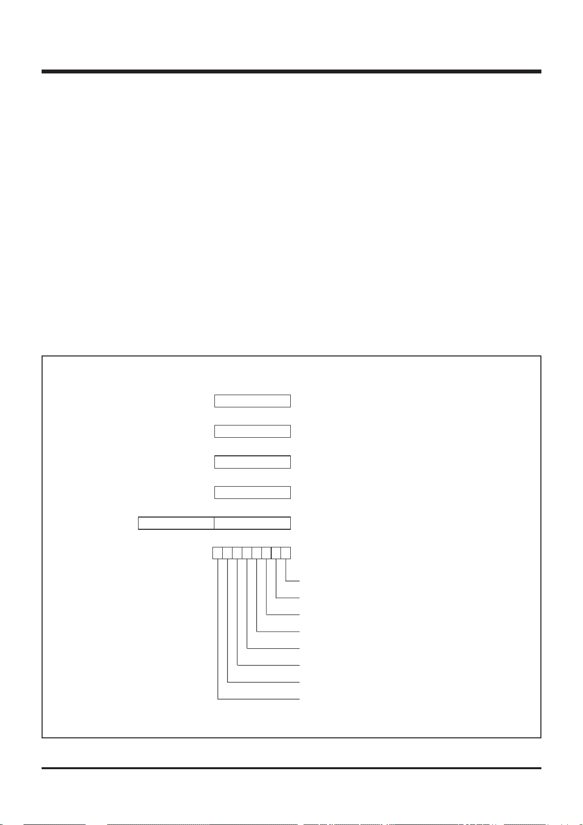
PART NUMBERING
Product
M3802 2 M 4 - XXX SP
Package type
SP : 64P4B package
FP : 64P6N-A package
SS : 64S1B-E package
FS : 64D0 package
ROM number
Omitted in some types.
Normally, using hyphen.
When electrical characteristic, or division of quality
identification code using alphanumeric character
– : standard
D : Extended operating temperature version
ROM/PROM size
: 4096 bytes
1
: 8192 bytes
2
: 12288 bytes
3
: 16384 bytes
4
: 20480 bytes
5
: 24576 bytes
6
: 28672 bytes
7
: 32768 bytes
8
Fig.4 Part numbering
The first 128 bytes and the last 2 bytes of ROM
are reserved areas ; they cannot be used.
Memory type
M
: Mask ROM version
E
: EPROM or One Time PROM version
RAM size
: 192 bytes
0
: 256 bytes
1
: 384 bytes
2
: 512 bytes
3
: 640 bytes
4
: 768 bytes
5
: 896 bytes
6
: 1024 bytes
7
1-6
3802 GROUP USER’S MANUAL
HARDWARE
GROUP EXPANSION
GROUP EXPANSION
Mitsubishi plans to expand the 3802 group as follows:
(1) Support for mask ROM, One Time PROM, and EPROM
versions
ROM/PROM capacity................................... 8 K to 32 K bytes
RAM capacity .............................................. 384 to 1024 bytes
Memory Expansion Plan
ROM size (bytes)
32K
28K
Mass product
24K
20K
Mass product
16K
12K
Mass product
8K
M38022M4
M38022M2
(2) Packages
64P4B ............................................ Shrink plastic molded DIP
64P6N-A................................................... Plastic molded QFP
64S1B-E.................................................... Shrink ceramic DIP
64D0................................................................... Ceramic LCC
Mass product
M38027M8/E8
M38024M6
4K
192
256 384 512 640 768 896 1024
Fig. 5 Memory expansion plan
Currently supported products are listed below
Table 2. List of supported products
Product
M38022M2-XXXSP
M38022M2-XXXFP
M38022M4-XXXSP
M38022M4-XXXFP
M38024M6-XXXSP
M38024M6-XXXFP
M38027M8-XXXSP
M38027E8-XXXSP
M38027E8SP
M38027M8-XXXFP
M38027E8-XXXFP
M38027E8FP
M38027E8SS
M38027E8FS
(P) ROM size (bytes)
ROM size for User in ( )
8192
(8062)
16384
(16254)
24576
(24446)
32768
(32638)
RAM size (bytes)
RAM size (bytes)
384
384
640
1024
Package
64P4B
64P6N-A
64P4B
64P6N-A
64P4B
64P6N-A
64P4B
64P6N-A
64S1B-E
64D0
As of May 1996
Remarks
Mask ROM version
Mask ROM version
Mask ROM version
Mask ROM version
Mask ROM version
Mask ROM version
Mask ROM version
One Time PROM version
One Time PROM version (blank)
Mask ROM version
One Time PROM version
One Time PROM version (blank)
EPROM version
EPROM version
3802 GROUP USER'S MANUAL
1-7
HARDWARE
GROUP EXPANSION
GROUP EXPANSION (Extended operating temperature version)
Mitsubishi plans to expand the 3802 group (extended operating
temperature version) as follows:
(1) Support for mask ROM One Time PROM, and EPROM ver-
sions
ROM/PROM capacity................................... 8 K to 32 K bytes
RAM capacity .............................................. 384 to 1024 bytes
(2) Packages
64P4B ............................................ Shrink plastic molded DIP
64P6N-A................................................... Plastic molded QFP
Memory Expansion Plan (Extended operating temperature version)
ROM size (bytes)
32K
28K
24K
20K
Mass product
16K
12K
Mass product
8K
M38022M4D
M38022M2D
Mass product
M38027M8D/E8D
4K
192
256 384 512 640 768 896 1024
RAM size (bytes)
Fig. 6 Memory expansion plan (Extended operating temperature version)
Currently supported products are listed below.
Table 3. List of supported products (Extended operating temperature version)
Product
M38022M2DXXXSP
M38022M2DXXXFP
M38022M4DXXXSP
M38022M4DXXXFP
M38027M8DXXXSP
M38027E8DXXXSP
M38027E8DSP
M38027M8DXXXFP
M38027E8DXXXFP
M38027E8DFP
(P) ROM size (bytes)
8192
(8062)
16384
(16254)
32768
(32638)
RAM size (bytes)
384
384
1024
Package
64P4B
64P6N-A
64P4B
64P6N-A
64P4B
64P6N-A
As of May 1996
Remarks
Mask ROM version
Mask ROM version
Mask ROM version
Mask ROM version
Mask ROM version
One Time PROM version
One Time PROM version (blank)
Mask ROM version
One Time PROM version
One Time PROM version (blank)
1-8
3802 GROUP USER’S MANUAL
HARDWARE
FUNCTIONAL DESCRIPTION
FUNCTIONAL DESCRIPTION
Central Processing Unit (CPU)
The 3802 group uses the standard 740 family instruction set. Refer
to the table of 740 family addressing modes and machine instructions or the SERIES 740 <Software> User´s Manual for details on
the instruction set.
Machine-resident 740 family instructions are as follows:
The FST and SLW instructions cannot be used.
The MUL, DIV, WIT and STP instruction can be used.
The central processing unit (CPU) has the six registers.
Accumulator (A)
The accumulator is an 8-bit register. Data operations such as data
transfer, etc., are executed mainly through the accumulator.
Index register X (X), Index register Y (Y)
Both index register X and index register Y are 8-bit registers. In the
index addressing modes, the value of the OPERAND is added to the
contents of register X or register Y and specifies the real address.
When the T flag in the processor status register is set to “1”, the
value contained in index register X becomes the address for the second OPERAND.
Stack pointer (S)
The stack pointer is an 8-bit register used during sub-routine calls
and interrupts. The stack is used to store the current address data
and processor status when branching to subroutines or interrupt routines.
The lower eight bits of the stack address are determined by the contents of the stack pointer. The upper eight bits of the stack address
are determined by the Stack Page Selection Bit. If the Stack Page
Selection Bit is “0”, then the RAM in the zero page is used as the
stack area. If the Stack Page Selection Bit is “1”, then RAM in page
1 is used as the stack area.
The Stack Page Selection Bit is located in the SFR area in the zero
page. Note that the initial value of the Stack Page Selection Bit varies with each microcomputer type. Also some microcomputer types
have no Stack Page Selection Bit and the upper eight bits of the
stack address are fixed. The operations of pushing register contents
onto the stack and popping them from the stack are shown in Fig.7.
Program counter (PC)
The program counter is a 16-bit counter consisting of two 8-bit registers
PC
H and PCL. It is used to indicate the address of the next instruction to
be executed.
b15
PC
b7
A
b7
X
b7
Y
b7
S
b7
H
b7
PC
b0
Accumulator
b0
Index Register X
b0
Index Register Y
b0
Stack Pointer
b0
L
Program Counter
b0
Processor Status Register (PS)
CZIDBTVN
Carry Flag
Zero Flag
Interrupt Disable Flag
Decimal Mode Flag
Break Flag
Index X Mode Flag
Fig. 7. 740 Family CPU register structure
Overflow Flag
Negative Flag
3802 GROUP USER’S MANUAL
1-9
HARDWARE
FUNCTIONAL DESCRIPTION
On-going Routine
Store Return Address
on Stack (Note 2)
Restore Return
Address
Interrupt request
M (S) (PCH)
(S)
M (S) (PCL)
(S)
Subroutine
Execute RTS
(S)
(PCL) M (S)
(S)
(PCH) M (S)
(S – 1)
(S – 1)
(S + 1)
(S + 1)
(Note 1)
Execute JSR
M (S) (PCH)
(S)
(S – 1)
M (S) (PCL)
(S)
(S – 1)
M (S) (PS)
(S)
(S – 1)
Interrupt
Service Routine
Execute RTI
(S)
(S + 1)
(PS) M (S)
(S)
(S + 1)
(PCL) M (S)
(S)
(S + 1)
Store Return Address
on Stack (Note 2)
Store Contents of Processor
Status Register on Stack
I Flag “0” to “1”
Fetch the Jump Vector
Restore Contents of
Processor Status Register
Restore Return
Address
Note 1 : The condition to enable the interrupt Interrupt enable bit is “1”
2 : When an interrupt occurs, the address of the next instruction to be executed is stored in
the stack area. When a subroutine is called, the address one before the next instruction
to be executed is stored in the stack area.
Fig. 8. Register push and pop at interrupt generation and subroutine call
Table. 4. Push and pop instructions of accumulator or processor status register
Push instruction to stack
Accumulator
Processor status register
PHA
PHP
Interrupt disable flag is “0”
(PCH) M (S)
Pop instruction from stack
PLA
PLP
1-10
3802 GROUP USER’S MANUAL

HARDWARE
FUNCTIONAL DESCRIPTION
Processor status register (PS)
The processor status register is an 8-bit register consisting of flags
which indicate the status of the processor after an arithmetic operation. Branch operations can be performed by testing the Carry (C)
flag, Zero (Z) flag, Overflow (V) flag, or the Negative (N) flag. In decimal mode, the Z, V, N flags are not valid.
After reset, the Interrupt disable (I) flag is set to “1”, but all other flags
are undefined. Since the Index X mode (T) and Decimal mode (D)
flags directly affect arithmetic operations, they should be initialized in
the beginning of a program.
(1) Carry flag (C)
The C flag contains a carry or borrow generated by the arithmetic
logic unit (ALU) immediately after an arithmetic operation. It can
also be changed by a shift or rotate instruction.
(2) Zero flag (Z)
The Z flag is set if the result of an immediate arithmetic operation
or a data transfer is “0”, and cleared if the result is anything other
than “0”.
(3) Interrupt disable flag (I)
The I flag disables all interrupts except for the interrupt
generated by the BRK instruction.
Interrupts are disabled when the I flag is “1”.
When an interrupt occurs, this flag is automatically set to “1” to
prevent other interrupts from interfering until the current interrupt
is serviced.
(4) Decimal mode flag (D)
The D flag determines whether additions and subtractions are
executed in binary or decimal. Binary arithmetic is executed when
this flag is “0”; decimal arithmetic is executed when it is “1”.
Decimal correction is automatic in decimal mode. Only the ADC
and SBC instructions can be used for decimal arithmetic.
(5) Break flag (B)
The B flag is used to indicate that the current interrupt was
generated by the BRK instruction. The BRK flag in the processor
status register is always “0”. When the BRK instruction is used to
generate an interrupt, the processor status register is pushed
onto the stack with the break flag set to “1”. The saved processor
status is the only place where the break flag is ever set.
(6) Index X mode flag (T)
When the T flag is “0”, arithmetic operations are performed
between accumulator and memory, e.g. the results of an
operation between two memory locations is stored in the
accumulator. When the T flag is “1”, direct arithmetic operations
and direct data transfers are enabled between memory locations,
i.e. between memory and memory, memory and I/O, and I/O and
I/O. In this case, the result of an arithmetic operation performed
on data in memory location 1 and memory location 2 is stored in
memory location 1. The address of memory location 1 is
specified by index register X, and the address of memory
location 2 is specified by normal addressing modes.
(7) Overflow flag (V)
The V flag is used during the addition or subtraction of one byte
of signed data. It is set if the result exceeds +127 to -128. When
the BIT instruction is executed, bit 6 of the memory location
operated on by the BIT instruction is stored in the overflow flag.
(8) Negative flag (N)
The N flag is set if the result of an arithmetic operation or data
transfer is negative. When the BIT instruction is executed, bit 7 of
the memory location operated on by the BIT instruction is stored
in the negative flag.
Table. 5. Set and clear instructions of each bit of processor status register
C flag Z flag I flag D flag B flag T flag V flag N flag
Set instruction
Clear instruction
SEC
CLC
_
_
SEI
CLI
SED
CLD
_
_
SET
CLT CLV
_
_
_
3802 GROUP USER’S MANUAL
1-11

HARDWARE
FUNCTIONAL DESCRIPTION
CPU Mode Register
The CPU mode register is allocated at address 003B16. The CPU mode
register contains the stack page selection bit.
b7
Fig. 9. Structure of CPU mode register
b0
CPU mode register
(
CPUM : address
003B16)
Processor mode bits
b1 b0
0 0 : Single-chip mode
0 1 : Memory expansion mode
1 0 : Microprocessor mode
1 1 : Not available
Stack page selection bit
0 : 0 page
1 : 1 page
Not used (return “0” when read)
1-12
3802 GROUP USER’S MANUAL
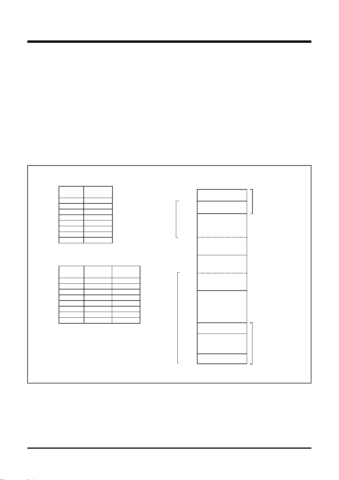
HARDWARE
FUNCTIONAL DESCRIPTION
Memory
Special function register (SFR) area
The Special Function Register area in the zero page contains control registers such as I/O ports and timers.
RAM
RAM is used for data storage and for stack area of subroutine
calls and interrupts.
ROM
The first 128 bytes and the last 2 bytes of ROM are reserved for
device testing and the rest is user area for storing programs.
Interrupt vector area
The interrupt vector area contains reset and interrupt vectors.
RAM area
RAM capacity
(bytes)
192
256
384
512
640
768
896
1024
Address
XXXX
00FF
013F
01BF
023F
02BF
033F
03BF
043F
16
16
16
16
16
16
16
16
16
Zero page
The 256 bytes from addresses 000016 to 00FF16 are called the
zero page area. The internal RAM and the special function registers (SFR) are allocated to this area.
The zero page addressing mode can be used to specify memory
and register addresses in the zero page area. Access to this area
with only 2 bytes is possible in the zero page addressing mode.
Special page
The 256 bytes from addresses FF0016 to FFFF16 are called the
special page area. The special page addressing mode can be
used to specify memory addresses in the special page area. Access to this area with only 2 bytes is possible in the special page
addressing mode.
0000
RAM
0040
0100
XXXX
16
16
16
16
SFR area
Zero page
Reserved area
ROM area
ROM capacity
(bytes)
4096
8192
12288
16384
20480
24576
28672
32768
Fig. 10 Memory map diagram
Address
YYYY
F000
E000
D000
C000
B000
A000
9000
8000
0440
16
Not used
16
16
16
16
16
16
16
16
16
Address
ZZZZ
F080
E080
D080
C080
B080
A080
9080
8080
16
16
16
16
16
16
16
16
16
ROM
YYYY
ZZZZ
FF00
FFDC
FFFE
FFFF
16
Reserved ROM area
(128 bytes)
16
16
16
Interrupt vector area
16
Reserved ROM area
16
Special page
3802 GROUP USER’S MANUAL
1-13

HARDWARE
FUNCTIONAL DESCRIPTION
Port P0 (P0)
0000
16
Port P0 direction register (P0D)
0001
16
Port P1 (P1)
0002
16
Port P1 direction register (P1D)
0003
16
Port P2 (P2)
0004
16
Port P2 direction register (P2D)
0005
16
Port P3 (P3)
0006
16
Port P3 direction register (P3D)
0007
16
Port P4 (P4)
0008
16
Port P4 direction register (P4D)
0009
16
Port P5 (P5)
000A
16
Port P5 direction register (P5D)
000B
16
Port P6 (P6)
000C
16
Port P6 direction register (P6D)
000D
16
000E
16
000F
16
0010
16
0011
16
0012
16
0013
16
0014
16
0015
16
0016
16
0017
16
Transmit/Receive buffer register (TB/RB)
0018
16
Serial I/O1 status register (SIO1STS)
0019
16
Serial I/O1 control register (SIO1CON)
001A
16
UART control register (UARTCON)
001B
16
Baud rate generator (BRG)
001C
16
Serial I/O2 control register (SIO2CON)
001D
16
001E
16
Serial I/O2 register (SIO2)
001F
16
Prescaler 12 (PRE12)
0020
16
Timer 1 (T1)
0021
16
Timer 2 (T2)
0022
16
Timer XY mode register (TM)
0023
16
Prescaler X (PREX)
0024
16
Timer X (TX)
0025
16
Prescaler Y (PREY)
0026
16
Timer Y (TY)
0027
16
0028
16
0029
16
002A
16
PWM control register (PWMCON)
002B
16
PMW prescaler (PREPWM)
002C
16
002D
16
PWM register (PWM)
002E
16
002F
16
0030
16
0031
16
0032
16
0033
16
AD/DA control register (ADCON)
0034
16
A-D conversion register (AD)
0035
16
D-A1 conversion register (DA1)
0036
16
D-A2 conversion register (DA2)
0037
16
0038
16
0039
16
Interrupt edge selection register
003A
16
CPU mode register (CPUM)
003B
16
Interrupt request register 1(IREQ1)
003C
16
Interrupt request register 2(IREQ2)
003D
16
Interrupt control register 1(ICON1)
003E
16
Interrupt control register 2(ICON2)
003F
16
(INTEDGE)
Fig. 11 Memory map of special function register (SFR)
1-14
3802 GROUP USER’S MANUAL
HARDWARE
FUNCTIONAL DESCRIPTION
I/O Ports
Direction registers
The 3802 group has 56 programmable I/O pins arranged in seven
I/O ports (ports P0 to P6). The I/O ports have direction registers
which determine the input/output direction of each individual pin.
Each bit in a direction register corresponds to one pin, each pin
can be set to be input port or output port.
When “0” is written to the bit corresponding to a pin, that pin becomes an input pin. When “1” is written to that bit, that pin becomes an output pin.
Table 6. list of I/O port functions
Pin
P00–P07
P10–P17
P20–P27
P30/DA1
P31/DA2
P32–P37
P40/INT4,
P41/INT0,
P43/INT2
P44/RXD,
P45/TXD,
P46/SCLK1,
P47/SRDY1
P50/SIN2,
P51/SOUT2,
P52/SCLK2,
P53/SRDY2
P54/CNTR0,
P55/CNTR1
P56/PWM
P57/INT3
P60/AN0–
P67/AN7
Note 1: For details of the functions of ports P0 to P3 in modes other than single-chip mode, and how to use double-function ports as func-
tion I/O ports, refer to the applicable sections.
2: Make sure that the input level at each pin is either 0 V or VCC during execution of the STP instruction.
When an input level is at an intermediate potential, a current will flow from VCC to VSS through the input-stage gate.
Name
Port P0
Port P1
Port P2
Port P3
Port P4
Port P5
Port P6
Input/Output
Input/output,
individual bits
Input/output,
individual bits
Input/output,
individual bits
Input/output,
individual bits
Input/output,
individual bits
Input/output,
individual bits
Input/output,
individual bits
I/O Format
CMOS 3-state output
CMOS compatible
input level
CMOS 3-state output
CMOS compatible
input level
CMOS 3-state output
CMOS compatible
input level
CMOS 3-state output
CMOS compatible
input level
CMOS 3-state output
CMOS compatible
input level
CMOS 3-state output
CMOS compatible
input level
CMOS 3-state output
CMOS compatible
input level
If data is read from a pin which is set to output, the value of the
port output latch is read, not the value of the pin itself. Pins set to
input are floating. If a pin set to input is written to, only the port
output latch is written to and the pin remains floating.
Non-Port Function
Address low-order byte
output
Address high-order
byte output
Data bus I/O
D-A conversion output
Control signal I/O
External interrupt input
Serial I/O1 function I/O
Serial I/O2 function I/O
Timer X and Timer Y
function I/O
PWM output
External interrupt input
A-D conversion input
Related SFRs
CPU mode register
CPU mode register
CPU mode register
AD/DA control register
CPU mode register
CPU mode register
Interrupt edge selection
register
Serial I/O1 control
register
UART control register
Serial I/O2 control
register
Timer XY mode register
PWM control register
Interrupt edge selection register
Ref.No.
(1)
(2)
(1)
(3)
(4)
(5)
(6)
(7)
(8)
(9)
(10)
(11)
(12)
(13)
(3)
(14)
3802 GROUP USER’S MANUAL
1-15

HARDWARE
FUNCTIONL DESCRIPTION
(1) Ports P0, P1, P2, P32–P37
Direction register
Data bus
Port latch
(3) Ports P40–P43, P57
Direction register
Data bus
Port latch
Interrupt input
(2) Ports P30, P31
Direction register
Data bus
Port latch
(4) Port P44
Serial I/O1 enable bit
Receive enable bit
Direction register
Data bus
Port latch
D–A conversion output
DA1 output enable bit (P30)
DA
2 output enable bit (P31)
Serial I/O1 input
(5) Port P45 (6) Port P46
P45/TXD P-channel output disable bit
Serial I/O1 enable bit
Transmit enable bit
Direction register
Data bus
Port latch
Serial I/O1 output
Serial I/O1 synchronous
clock selection bit
Serial I/O1 enable bit
Serial I/O1 mode selection bit
Data bus
(7) Port P47 (8) Port P50
Serial I/O1 mode selection bit
Serial I/O1 enable bit
S
RDY1 output enable bit
Data bus
Direction register
Port latch
Data bus
Serial I/O1 enable bit
Direction register
Port latch
Serial I/O1 clock output
Direction register
Port latch
Serial I/O2 input
Serial I/O1
external
clock input
Serial I/O1 ready output
Fig. 12 Port block diagram (single-chip mode) (1)
1-16
3802 GROUP USER’S MANUAL

HARDWARE
FUNCTIONAL DESCRIPTION
(9) Port P5
Data bus
(11) Port P5
1
P5
1/SOUT2
Serial I/O2 transmit end signal
Serial I/O2 port selection bit
Direction register
Port latch
Serial I/O2 output
3
Data bus
Serial I/O2 ready output
P-channel output disable bit
S
RDY2
output enable bit
Direction register
Port latch
(10) Port P5
Data bus
2
Serial I/O2
synchronous clock selection bit
Serial I/O2 port selection bit
Serial I/O2 clock output
(12) Ports P54, 5
Data bus
Direction register
Port latch
5
Direction register
Port latch
Pulse output mode
Timer output
Serial I/O2 external clock input
CNTR
0
, CNTR
Interrupt input
1
6
PWM output enable bit
Direction register
Data bus
Port latch
PWM output
Fig. 13 Port block diagram (single-chip mode) (2)
(14) Port P6(13) Port P5
Data bus
Direction register
Port latch
A-D conversion input
Analog input pin selection bit
3802 GROUP USER’S MANUAL
1-17

HARDWARE
FUNCTIONAL DESCRIPTION
INTERRUPTS
Interrupts occur by sixteen sources: seven external, eight internal,
and one software.
Interrupt control
Each interrupt is controlled by an interrupt request bit, an interrupt
enable bit, and the interrupt disable flag except for the software interrupt set by the BRK instruction. An interrupt occurs if the corresponding interrupt request and enable bits are “1” and the interrupt disable flag is “0”.
Interrupt enable bits can be set or cleared by software.
Interrupt request bits can be cleared by software, but cannot be
set by software.
The BRK instruction cannot be disabled with any flag or bit. The I
(interrupt disable) flag disables all interrupts except the BRK instruction interrupt.
When several interrupts occur at the same time, the interrupts are
received according to priority.
Table 7. Interrupt vector addresses and priority
Interrupt Source
Reset (Note 2)
INT
0
INT1
Serial I/O1
reception
Serial I/O1
transmission
Timer X
Timer Y
Timer 1
Timer 2
0
CNTR
CNTR1
Serial I/O2
INT2
INT3
INT4
A-D converter
Priority
1
2
3
4
5
6
7
8
9
10
11
12
13
14
15
16
Vector Addresses (Note 1)
High
FFFD16
FFFB16
FFF916
FFF716
FFF516
FFF316
FFF116
FFEF16
FFED16
FFEB16
FFE916
FFE716
FFE516
FFE316
FFE116
FFDF16
Low
FFFC
FFFA16
FFF816
FFF616
FFF416
FFF216
FFF016
FFEE16
FFEC16
FFEA16
FFE816
FFE616
FFE416
FFE216
FFE016
FFDE16
16
Interrupt operation
When an interrupt is received, the contents of the program counter
and processor status register are automatically stored into the
stack. The interrupt disable flag is set to inhibit other interrupts
from interfering.The corresponding interrupt request bit is cleared
and the interrupt jump destination address is read from the vector
table into the program counter.
Notes on use
When the active edge of an external interrupt (INT0 to INT4,
CNTR
0, or CNTR1) is changed, the corresponding interrupt re-
quest bit may also be set. Therefore, please take following sequence;
(1) Disable the external interrupt which is selected.
(2) Change the active edge selection.
(3) Clear the interrupt request bit which is selected to “0”.
(4) Enable the external interrupt which is selected.
Interrupt Request
Generating Conditions
At reset
At detection of either rising or
falling edge of INT
At detection of either rising or
falling edge of INT1 input
At completion of serial I/O1
data reception
At completion of serial I/O1
transfer shift or when
transmission buffer is empty
At timer X underflow
At timer Y underflow
At timer 1 underflow
At timer 2 underflow
At detection of either rising or
falling edge of CNTR0 input
At detection of either rising or
falling edge of CNTR1 input
At completion of serial I/O2
data transfer
At detection of either rising or
falling edge of INT2 input
At detection of either rising or
falling edge of INT3 input
At detection of either rising or
falling edge of INT4 input
At completion of A-D conversion
0 input
Non-maskable
External interrupt
(active edge selectable)
External interrupt
(active edge selectable)
Valid when serial I/O1 is selected
Valid when serial I/O1 is selected
STP release timer underflow
External interrupt
(active edge selectable)
External interrupt
(active edge selectable)
Valid when serial I/O2 is selected
External interrupt
(active edge selectable)
External interrupt
(active edge selectable)
External interrupt
(active edge selectable)
Remarks
BRK instruction
Note 1: Vector addresses contain interrupt jump destination addresses.
2: Reset function in the same way as an interrupt with the highest priority.
17
FFDD16
1-18
FFDC16
3802 GROUP USER’S MANUAL
At BRK instruction execution
Non-maskable software interrupt

Interrupt request bit
Interrupt enable bit
Interrupt disable flag (I)
HARDWARE
FUNCTIONAL DESCRIPTION
Fig. 14 Interrupt control
b7 b0
b7 b0
BRK instruction
Interrupt edge selection register
16
(INTEDGE : address 003A
)
INT0 active edge selection bit
INT
1
active edge selection bit
Not used (returns “0” when read)
INT
2
active edge selection bit
INT
3
active edge selection bit
INT
4
active edge selection bit
Not used (returns “0” when read)
Interrupt request register 1
(IREQ1 : address 003C
16
)
INT0 interrupt request bit
INT
1
interrupt request bit
Serial I/O1 receive interrupt request bit
Serial I/O1 transmit interrupt request bit
Timer X interrupt request bit
Timer Y interrupt request bit
Timer 1 interrupt request bit
Timer 2 interrupt request bit
Reset
0 : Falling edge active
1 : Rising edge active
b7 b0
Interrupt request
Interrupt request register 2
(IREQ2 : address 003D
CNTR0 interrupt request bit
CNTR
1
interrupt request bit
Serial I/O2 interrupt request bit
INT2 interrupt request bit
INT
3
interrupt request bit
INT
4
interrupt request bit
AD converter interrupt request bit
Not used (returns “0” when read)
0 : No interrupt request issued
1 : Interrupt request issued
16
)
b7 b0
Interrupt control register 1
(ICON1 : address 003E
INT0 interrupt enable bit
INT
1
interrupt enable bit
Serial I/O1 receive interrupt enable bit
Serial I/O1 transmit interrupt enable bit
Timer X interrupt enable bit
Timer Y interrupt enable bit
Timer 1 interrupt enable bit
Timer 2 interrupt enable bit
Fig. 15 Structure of interrupt-related registers
b7 b0
16
)
3802 GROUP USER’S MANUAL
Interrupt control register 2
(ICON2 : address 003F16)
CNTR0 interrupt enable bit
CNTR
1
interrupt enable bit
Serial I/O2 interrupt enable bit
INT
2
interrupt enable bit
INT
3
interrupt enable bit
INT
4
interrupt enable bit
AD converter interrupt enable bit
Not used (returns “0” when read)
(Do not write “1” to this bit)
0 : Interrupts disabled
1 : Interrupts enabled
1-19

HARDWARE
FUNCTIONAL DESCRIPTION
Timers
The 3802 group has four timers: timer X, timer Y, timer 1, and timer
2.
All timers are count down. When the timer reaches “00
derflow occurs at the next count pulse and the corresponding
timer latch is reloaded into the timer and the count is continued.
When a timer underflows, the interrupt request bit corresponding
to that timer is set to “1”.
The division ratio of each timer or prescaler is given by 1/(n + 1),
where n is the value in the corresponding timer or prescaler latch.
b7
b0
Timer XY mode register
(TM : address 0023
Timer X operating mode bit
b1b0
0 0: Timer mode
0 1: Pulse output mode
1 0: Event counter mode
1 1: Pulse width measurement mode
CNTR0 active edge switch bit
0: Interrupt at falling edge
Count at rising edge in event
counter mode
1: Interrupt at rising edge
Count at falling edge in event
counter mode
Timer X count stop bit
0: Count start
1: Count stop
Timer Y operating mode bit
b4b5
0 0: Timer mode
0 1: Pulse output mode
1 0: Event counter mode
1 1: Pulse width measurement mode
CNTR
1
active edge switch bit
0: Interrupt at falling edge
Count at rising edge in event
counter mode
1: Interrupt at rising edge
Count at falling edge in event
counter mode
Timer Y count stop bit
0: Count start
1: Count stop
16”, an un-
16)
Timer 1 and Timer 2
The count source of prescaler 12 is the oscillation frequency divided by 16. The output of prescaler 12 is counted by timer 1 and
timer 2, and a timer underflow sets the interrupt request bit.
Timer X and Timer Y
Timer X and Timer Y can each be selected in one of four operating
modes by setting the timer XY mode register.
Timer Mode
The timer counts f(X
Pulse Output Mode
Timer X (or timer Y) counts f(X
the timer reach “00
CNTR
1) pin is inverted. If the CNTR0 (or CNTR1) active edge
switch bit is “0”, output begins at “ H”.
If it is “1”, output starts at “L”. When using a timer in this mode, set
the corresponding port P5
put mode.
Event Counter Mode
Operation in event counter mode is the same as in timer mode,
except the timer counts signals input through the CNTR
CNTR
1 pin.
Pulse Width Measurement Mode
If the CNTR
0 (or CNTR1) active edge selection bit is “0”, the timer
counts at the oscillation frequency divided by 16 while the CNTR
(or CNTR1) pin is at “H”. If the CNTR0 (or CNTR1) active edge
switch bit is “1”, the count continues during the time that the
CNTR
0 (or CNTR1) pin is at “L”.
In all of these modes, the count can be stopped by setting the
timer X (timer Y) count stop bit to “1”. Every time a timer
underflows, the corresponding interrupt request bit is set.
IN)/16 in timer mode.
IN)/16. Whenever the contents of
16”, the signal output from the CNTR0 (or
4 ( or port P55) direction register to out-
0 or
0
Fig. 16 Structure of timer XY register
1-20
3802 GROUP USER’S MANUAL

Oscillator Divider
f(X
P54/CNTR0 pin
Port P5
direction register
IN) 1/16
CNTR
0 active
edge switch bit
“0”
“1”
4
Port P5
latch
Pulse output
mode
Pulse width
measurement
mode
Event
counter
mode
0 active
CNTR
edge switch
bit
4
Timer mode
Pulse output
mode
Timer X count stop bit
Q
“1”
“0”
Toggle flip- flop T
Q
Data bus
Prescaler X latch (8)
Prescaler X (8)
R
Data bus
HARDWARE
FUNCTIONAL DESCRIPTION
Timer X latch (8)
Timer X (8)
Timer X latch write pulse
Pulse output mode
To timer X interrupt
request bit
0 interrupt
To CNTR
request bit
P55/CNTR1 pin
Port P5
direction register
CNTR1 active
edge switch bit
“0”
“1”
5
Pulse output
mode
Port P5
latch
Pulse width
measurement
mode
Event
counter
mode
1 active
CNTR
edge switch
bit
5
Timer mode
Pulse output
mode
Timer Y count stop bit
Q
“1”
“0”
Prescaler
12 latch (8)
Toggle flip- flop T
Q
Prescaler Y latch (8)
Prescaler Y (8)
R
Data bus
Timer Y latch (8)
Timer Y (8)
Timer Y latch write pulse
Pulse output mode
Timer 2 latch (8) Timer 1 latch (8)
To timer Y interrupt
request bit
To CNTR
1 interrupt
request bit
Prescaler 12 (8)
Fig. 17 Block diagram of timer X, timer Y, timer 1, and timer 2
3802 GROUP USER’S MANUAL
Timer 2 (8)Timer 1 (8)
To timer 2 interrupt
request bit
To timer 1 interrupt
request bit
1-21

HARDWARE
FUNCTIONAL DESCRIPTION
Serial I/O
Serial I/O1
Serial I/O1 can be used as either clock synchronous or asynchronous (UART) serial I/O. A dedicated timer is also provided for
baud rate generation.
Data bus
Clock synchronous serial I/O mode
Clock synchronous serial I/O1 mode can be selected by setting
the mode selection bit of the serial I/O1 control register to “1”.
For clock synchronous serial I/O1, the transmitter and the receiver
must use the same clock. If an internal clock is used, transfer is
started by a write signal to the TB/RB (address 0018
16).
Receive buffer
P44/RXD
P46/S
7/SRDY1
P4
5/TX
P4
CLK1
f(XIN)
X
BRG count source selection bit
IN
F/F
D
1/4
Falling-edge detector
Receive shift register
Transmit shift register
Fig. 18 Block diagram of clock synchronous serial I/O1
Transfer shift clock
(1/2 to 1/2048 of the internal
clock, or an external clock)
Serial output TxD
D0 D1 D2 D3 D4 D5 D6
Address 0018
Shift clock
Serial I/O1 synchronous
clock selection bit
Frequency division ratio 1/(n+1)
Baud rate generator
Transmit buffer
Data bus
16
Address 001C
Shift clock
Address 0018
Serial I/O1 control register
Receive buffer full flag (RBF)
Receive interrupt request (RI)
Clock control circuit
1/4
16
Clock control circuit
Transmit shift completion flag (TSC)
Transmit interrupt source selection bit
Serial I/O1 status register
16
Transmit buffer empty flag (TBE)
Address 001A
Transmit interrupt request (TI)
Address 0019
16
16
D7
Serial input RxD
Receive enable signal SRDY1
Write pulse to receive/transmit
buffer (address 0018
Notes
16)
1 : The transmit interrupt (TI) can be selected to occur either when the transmit buffer has emptied (TBE=1) or after the
transmit shift operation has ended (TSC=1), by setting the transmit interrupt source selection bit (TIC) of the serial I/O1
control register.
2 : If data is written to the transmit buffer when TSC=0, the transmit clock is generated continuously and serial data is
output continuously from the TxD pin.
3 : The receive interrupt (RI) is set when the receive buffer full flag (RBF) becomes “1” .
TBE = 0
D0 D1 D2 D3 D4 D5 D6
TBE = 1
TSC = 0
Fig. 19 Operation of clock synchronous serial I/O1 function
1-22
3802 GROUP USER’S MANUAL
D7
RBF = 1
TSC = 1
Overrun error (OE)
detection

HARDWARE
FUNCTIONAL DESCRIPTION
Asynchronous serial I/O (UART) mode
Clock asynchronous serial I/O mode (UART) can be selected by
clearing the serial I/O mode selection bit of the serial I/O control
register to “0”.
Eight serial data transfer formats can be selected, and the transfer
formats used by a transmitter and receiver must be identical.
The transmit and receive shift registers each have a buffer, but the
Data bus
P4
P4
P4
4/RX
6/SCLK1
f(XIN)
5/TX
D
STdetector
BRG count source selection bit
D
Character length selection bit
1/4
Character length selection bit
Address 0018
OE
7 bits
8 bits
Serial I/O1 synchronous clock selection bit
16
Receive buffer
Receive shift register
PE FE
SP detector
Frequency division ratio 1/(n+1)
Baud rate generator
Address 001C
ST/SP/PA generator
Transmit shift register
Transmit buffer
Data bus
two buffers have the same address in memory. Since the shift register cannot be written to or read from directly, transmit data is
written to the transmit buffer, and receive data is read from the receive buffer.
The transmit buffer can also hold the next data to be transmitted,
and the receive buffer can hold a character while the next character is being received.
Serial I/O1 control register
Receive buffer full flag (RBF)
Receive interrupt request (RI)
Clock control circuit
16
1/16
Transmit interrupt source selection bit
Address
0018
Serial I/O1 status register
16
Address 001A
1/16
16
UART control register
Address 001B
Transmit shift completion flag (TSC)
Transmit interrupt request (TI)
Transmit buffer empty flag (TBE)
Address
0019
16
16
Fig. 20 Block diagram of UART serial I/O
3802 GROUP USER’S MANUAL
1-23

HARDWARE
FUNCTIONAL DESCRIPTION
Transmit or receive clock
Transmit buffer write
Receive buffer read
signal
TBE=0 TBE=0
TSC=0
TBE=1
Serial output TXD
signal
Serial input R
Notes
X
D
1: Error flag detection occurs at the same time that the RBF flag becomes "1" (at 1st stop bit, during reception).
2: The transmit interrupt (TI) can be selected to occur when either the TBE or TSC flag becomes "1", depending on the setting of the transmit interrupt
source selection bit (TIC) of the serial I/O control register.
3: The receive interrupt (RI) is set when the RBF flag becomes "1".
4: After data is written to the transmit buffer when TSC=1, 0.5 to 1.5 cycles of the data shift cycle is necessary until changing to TSC=0.
ST SP
D
0
D
1
1 start bit
7 or 8 data bit
1 or 0 parity bit
1 or 2 stop bit (s)
ST
D
0
D
1
Fig. 21 Operation of UART serial I/O function
Serial I/O1 control register (SIO1CON) 001A16
The serial I/O control register consists of eight control bits for the
serial I/O function.
UART control register (UARTCON) 001B16
The UART control register consists of four control bits (bits 0 to 3)
which are valid when asynchronous serial I/O is selected and set
the data format of an data transfer. One bit in this register (bit 4) is
always valid and sets the output structure of the P4
5/TXD pin.
Serial I/O1 status register (SIO1STS) 001916
The read-only serial I/O1 status register consists of seven flags
(bits 0 to 6) which indicate the operating status of the serial I/O
function and various errors.
Three of the flags (bits 4 to 6) are valid only in UART mode.
The receive buffer full flag (bit 1) is cleared to “0” when the receive
buffer is read.
If there is an error, it is detected at the same time that data is
transferred from the receive shift register to the receive buffer, and
the receive buffer full flag is set. A write to the serial I/O status register clears all the error flags OE, PE, FE, and SE (bit 3 to bit 6, re-
TBE=1
ST
SP
RBF=1
ST
SP D
D
0
D
1
✽
Generated at 2nd bit in 2-stop-bit mode
RBF=0
D
1
0
TSC=1
RBF=1
SP
✽
spectively). Writing “0” to the serial I/O enable bit SIOE (bit 7 of
the Serial I/O Control Register) also clears all the status flags, including the error flags.
All bits of the serial I/O1 status register are initialized to “0” at reset, but if the transmit enable bit (bit 4) of the serial I/O control register has been set to “1”, the transmit shift completion flag (bit 2)
and the transmit buffer empty flag (bit 0) become “1”.
Transmit buffer/Receive buffer register (TB/
RB) 0018
The transmit buffer and the receive buffer are located at the same
address. The transmit buffer is write-only and the receive buffer is
read-only. If a character bit length is 7 bits, the MSB of data stored
in the receive buffer is “0”.
16
Baud rate generator (BRG) 001C16
The baud rate generator determines the baud rate for serial transfer.
The baud rate generator divides the frequency of the count source
by 1/(n + 1), where n is the value written to the baud rate generator.
1-24
3802 GROUP USER’S MANUAL

HARDWARE
FUNCTIONAL DESCRIPTION
b7
b0
Serial I/O1 status register
(SIO1STS : address 0019
16
)
b7
Transmit buffer empty flag (TBE)
0: Buffer full
1: Buffer empty
Receive buffer full flag (RBF)
0: Buffer empty
1: Buffer full
Transmit shift completion flag (TSC)
0: Transmit shift in progress
1: Transmit shift completed
Overrun error flag (OE)
0: No error
1: Overrun error
Parity error flag (PE)
0: No error
1: Parity error
Framing error flag (FE)
0: No error
1: Framing error
Summing error flag (SE)
0: (OE) U (PE) U (FE)=0
1: (OE) U (PE) U (FE)=1
Not used (returns "1" when read)
b0
Serial I/O1 control register
(SIO1CON : address 001A16)
BRG count source selection bit (CSS)
0: f(X
IN
)
1: f(X
IN
)/4
Serial I/O1 synchronous clock selection bit (SCS)
0: BRG output divided by 4 when clock synchronous
serial I/O is selected, BRG output divided by 16
when UART is selected.
1: External clock input when clock synchronous serial
I/O is selected, external clock input divided by 16
when UART is selected.
S
RDY1
output enable bit (SRDY)
0: P4
7
pin operates as ordinaly I/O pin
1: P4
7
pin operates as S
RDY1
output pin
Transmit interrupt source selection bit (TIC)
0: Interrupt when transmit buffer has emptied
1: Interrupt when transmit shift operation is completed
Transmit enable bit (TE)
0: Transmit disabled
1: Transmit enabled
Receive enable bit (RE)
0: Receive disabled
1: Receive enabled
Serial I/O1 mode selection bit (SIOM)
0: Asynchronous serial I/O (UART)
1: Clock synchronous serial I/O
b7
b0
UART control register
(UARTCON : address 001B
Character length selection bit (CHAS)
0: 8 bits
1: 7 bits
16
)
Serial I/O enable bit (SIOE)
0: Serial I/O disabled
(pins P4
4
to P47 operate as ordinary I/O pins)
1: Serial I/O enabled
(pins P4
4
to P47 operate as serial I/O pins)
Parity enable bit (PARE)
0: Parity checking disabled
1: Parity checking enabled
Parity selection bit (PARS)
0: Even parity
1: Odd parity
Stop bit length selection bit (STPS)
0: 1 stop bit
1: 2 stop bits
P4
5/TX
D P-channel output disable bit (POFF)
0: CMOS output (in output mode)
1: N-channel open drain output (in output mode)
Not used (return "1" when read)
Fig. 22 Structure of serial I/O control registers
3802 GROUP USER’S MANUAL
1-25

HARDWARE
Serial I/O2 control register
(SIO2CON : address 001D
16
)
b7
Internal synchronous clock selection bits
0 0 0: f(XIN)/8
0 0 1: f(X
IN
)/16
0 1 0: f(X
IN
)/32
0 1 1: f(X
IN
)/64
1 1 0: f(X
IN
)/128
1 1 1: f(X
IN
)/256
Serial I/O2 port selection bit (SM2
3
)
0: I/O port
1: S
OUT2,SCLK2
output pin
S
RDY2
output enable bit (SM24)
0: I/O port
1: S
RDY2
output pin
Transfer direction selection bit (SM2
5
)
0: LSB first
1: MSB first
Serial I/O2 synchronous clock selection bit (SM2
6
)
0: External clock
1: Internal clock
P5
1/SOUT2
P-channel output disable bit
0: CMOS output (in output mode)
1: N-channel open-drain output (in output mode)
b0
b2 b1 b0
FUNCTIONAL DESCRIPTION
Serial I/O2
The serial I/O2 function can be used only for clock synchronous
serial I/O.
For clock synchronous serial I/O the transmitter and the receiver
must use the same clock. If the internal clock is used, transfer is
started by a write signal to the serial I/O2 register.
Serial I/O2 control register (SIO2CON) 001D16
The serial I/O2 control register contains seven bits which control
various serial I/O functions.
Fig. 23 Structure of serial I/O2 control register
1/8
1/16
X
IN
P53 latch
S
RDY2
P52 latch
"0"
"1"
P5
"0"
"0"
"1"
output enable bit
1
latch
"1"
P53/S
RDY2
P52/S
CLK2
Serial I/O2 port selection bit
P51/S
OUT2
Fig. 24 Block diagram of serial I/O2 function
P50/S
Serial I/O2 port selection bit
IN2
Serial I/O2 synchronous
S
RDY2
clock selection bit
Synchronization circuit
CLK2
S
External clock
1/32
1/64
Divider
1/128
1/256
"1"
"0"
Serial I/O counter 2 (3)
Serial I/O shift register 2 (8)
Internal synchronous
clock selection bits
Data bus
Serial I/O2
interrupt request
1-26
3802 GROUP USER’S MANUAL

Transfer clock (Note 1)
Serial I/O2 register
write signal
Serial I/O2 output S
Serial I/O2 input SIN2
Receive enable signal SRDY2
Notes
OUT2
1:
When the internal clock is selected as the transfer clock, the divide ratio can be selected by setting bits 0 to 2 of the serial
I/O2 control register.
2:
When the internal clock is selected as the transfer clock, the S
Fig. 25 Timing of serial I/O2 function
D2
HARDWARE
FUNCTIONAL DESCRIPTION
(Note 2)
D3 D4 D5 D6
Serial I/O2 interrupt request bit set
OUT2 pin goes to high impedance after transfer completion.
D7D0 D1
3802 GROUP USER’S MANUAL
1-27

HARDWARE
FUNCTIONAL DESCRIPTION
PULSE WIDTH MODULATION (PWM)
The 3802 group has a PWM function with an 8-bit resolution,
based on a signal that is the clock input X
vided by 2.
IN or that clock input di-
Data Setting
The PWM output pin also functions as port P56. Set the PWM period by the PWM prescaler, and set the period during which the
output pulse is an “H” by the PWM register.
If the value in the PWM prescaler is n and the value in the PWM
register is m (where n = 0 to 255 and m = 0 to 255) :
PWM period = 255 ✕ (n+1)/f(X
= 51 ✕ (n+1) µs (when X
Output pulse “H” period = PWM period ✕ m/255
IN)
IN = 5 MHz)
= 0.2 ✕ (n+1) ✕ m µs
(when X
IN = 5 MHz)
PWM Operation
When bit 0 (PWM enable bit) of the PWM control register is set to
“1”, operation starts by initializing the PWM output circuit, and
pulses are output starting at an “H”.
If the PWM register or PWM prescaler is updated during PWM
output, the pulses will change in the cycle after the one in which
the change was made.
51 ✕ m ✕ (n+1)
255
PWM output
T = [51 ✕ (n+1)] µs
m: Contents of PWM register
n : Contents of PWM prescaler
T : PWM cycle (when X
Fig. 26 Timing of PWM cycle
IN
= 5 MHz)
µs
Data bus
prescaler pre-latch
Count source
selection bit
1/2
“0”
“1”
XIN
Fig. 27 Block diagram of PWM function
PWM
Transfer control circuit
PWM
prescaler latch
PWM prescaler
PWM
register pre-latch
PWM
register latch
PWM register
Port P56 latch
PWM enable bit
Port P5
6
1-28
3802 GROUP USER’S MANUAL

HARDWARE
FUNCTIONAL DESCRIPTION
b7
Fig. 28 Structure of PWM control register
PWM output
b0
PWM control register
(PWMCON : address 002B
PWM function enable bit
0: PWM disabled
1: PWM enabled
Count source selection bit
IN
)
0: f(X
IN
)/2
1: f(X
Not used (return “0” when read)
ABC
16
)
C
B
=
T2
T
T
T
T2
PWM register
write signal
PWM prescaler
write signal
When the contents of the PWM register or PWM prescaler have changed, the PWM
output will change from the next period after the change.
Fig. 29 PWM output timing when PWM register or PWM prescaler is changed
(Changes from “A” to “B” during “H” period)
(Changes from “T” to “T2” during PWM period)
3802 GROUP USER’S MANUAL
1-29

HARDWARE
FUNCTIONAL DESCRIPTION
A-D Converter
The functional blocks of the A-D converter are described below.
[A-D conversion register]
The A-D conversion register is a read-only register that stores the
result of an A-D conversion. When reading this register during an
A-D conversion, the previous conversion result is read.
[AD/DA control register]
The AD/DA control register controls the A-D conversion process.
Bits 0 to 2 select a specific analog input pin. Bit 3 signals the
completion of an A-D conversion. The value of this bit remains at
“0” during an A-D conversion, and changes to “1” when an A-D
conversion ends. Writing “0” to this bit starts the A-D conversion.
Bits 6 and 7 are used to control the output of the D-A converter.
[Comparison voltage generator]
The comparison voltage generator divides the voltage between
AV
SS and VREF into 256, and outputs the divided voltages.
[Channel selector]
The channel selector selects one of the ports P60/AN0 to P67/AN7,
and inputs the voltage to the comparator.
[Comparator and Control circuit]
The comparator and control circuit compares an analog input voltage with the comparison voltage, then stores the result in the A-D
conversion register. When an A-D conversion is complete, the
control circuit sets the AD conversion completion bit and the AD
interrupt request bit to “1”.
Note that the comparator is constructed linked to a capacitor, so
set f(X
IN) to 500 kHz or more during an A-D conversion.
b7
b0
AD/DA control register
(ADCON : address 0034
Analog input pin selection bits
b2 b1 b0
0 0 0: P6
0 0 1: P61/AN1
0 1 0: P62/AN2
0 1 1: P63/AN3
1 0 0: P64/AN4
1 0 1: P65/AN5
1 1 0: P66/AN6
1 1 1: P67/AN7
AD conversion completion bit
0: Conversion in progress
1: Conversion completed
Not used (return "0" When read)
DA
0: DA
1: DA
DA
0: DA
1: DA
0/AN0
1 output enable bit
1 output disabled
1 output enabled
2 output enable bit
2 output disabled
2 output enabled
16)
AD/DA control register
(Address 0034
P60/AN
P61/AN
P62/AN
P63/AN
P64/AN
P65/AN
P66/AN
P67/AN
16
0
1
2
3
4
5
6
7
Fig. 31 Block diagram of A-D converter
b7 b0
)
3
Comparator
Channel selector
Fig.30 Structure of AD/DA control register
Data bus
A-D control circuit
A-D conversion register
Resistor ladder
REF
V
AV
A-D interrupt request
16
(Address 0035
)
8
SS
1-30
3802 GROUP USER’S MANUAL

D-A Converter
P30/DA
1
D-A1 conversion register (8)
R-2R resistor ladder
DA
1
output enable bit
P3
1
/DA
2
D-A2 conversion register (8)
R-2R resistor ladder
DA
2
output enable bit
Data bus
The 3802 group has two internal D-A converters (DA1 and DA2)
with 8-bit resolutions.
The D-A converter is performed by setting the value in the D-A
conversion register. The result of D-A converter is output from the
DA
1 or DA2 pin by setting the DA output enable bit to “1”.
When using the D-A converter, the corresponding port direction
register bit (P3
tus).
The output analog voltage V is determined by the value n (base
10) in the D-A conversion register as follows:
V = V
REF ✕ n/256 (n = 0 to 255)
Where V
At reset, the D-A conversion registers are cleared to “0016”, the DA
output enable bits are cleared to “0”, and the P3
DA
2 pins are set to input (high impedance).
The D-A output is not buffered, so connect an external buffer when
driving a low-impedance load.
Set V
CC to 3.0 V or more when using the D-A converter.
0/DA1 or P31/DA2) should be set to “0” (input sta-
REF is the reference voltage.
0/DA1 and P31/
HARDWARE
FUNCTIONAL DESCRIPTION
DA
1
"0"
P30/DA1
"1"
D-A1 conversion
register
AV
SS
V
REF
Fig. 33 Equivalent connection circuit of D-A converter
output enable bit
R
2R
MSB
"0"
"1"
2R
Fig. 32 Block diagram of D-A converter
R
2R
R
2R
R
R
2R
R
2R
R
2R 2R
LSB
2R
3802 GROUP USER’S MANUAL
1-31

HARDWARE
FUNCTIONAL DESCRIPTION
Reset Circuit
To reset the microcomputer, the RESET pin should be held at an
“L” level for 2 µs or more. Then the RESET pin is returned to an “H”
level (the power source voltage should be between 4.0 V and 5.5
V), reset is released. Internal operation begin until after 8 to 13 X
clock cycles are completed. After the reset is completed, the program starts from the address contained in address FFFD
order byte) and address FFFC
16 (low-order byte).
Make sure that the reset input voltage is less than 0.6 V for V
3.0 V (Extended operating temperature version : the reset input
voltage is less than 0.8 V for V
CC of 4.0 V).
4.0V
Power source
voltage
Reset input
voltage
0V
0V
1
M51953AL
3
5
4
0.1 µ F
0.8V
V
CC
RESET
SS
V
3802 group
Fig. 34 Example of reset circuit
16 (high-
CC of
Address
(1)
Port P0 direction register
(2)
IN
Port P1 direction register
(3)
Port P2 direction register
(4)
Port P3 direction register
(5)
Port P4 direction register
(6)
Port P5 direction register
(7)
Port P6 direction register
Serial I/O1 status register
(8)
(9)
Serial I/O1 control register
(10)
UART control register
(11)
Serial I/O2 control register
(12)
Prescaler 12
(13)
Timer 1
Timer 2
(14)
(15)
Timer XY mode register
(16)
Prescaler X
(17)
Timer X
(18)
Prescaler Y
(19)
Timer Y
(20)
PWM control register
(21)
AD/DA control register
(22)
D-A1 conversion register
D-A2 conversion register
(23)
(24)
Interrupt edge selection register
(25)
CPU mode register
Interrupt request register 1
(26)
Interrupt request register 2
(27)
Interrupt control register 1
(28)
(29)
Interrupt control register 2
(30)
Processor status register
Program counter
(31)
(000116) · · ·
(0003
(0005
(0007
(0009
(000B
(000D
(0019
(001A
(001B
(001D
(0020
(0021
(0022
(0023
(0024
(0025
(0026
(0027
(002B
(0034
(0036
(0037
(003A
(003B
(003C
(003D
(003E
(003F16) · · ·
Register contents
16) · · ·
16) · · ·
16) · · ·
16) · · ·
16) · · ·
16) · · ·
16) · · ·
100000 00
16) · · ·
16) · · ·
111000 00
16) · · ·
16) · · ·
16) · · ·
16) · · ·
16) · · ·
16) · · ·
16) · · ·
16) · · ·
16) · · ·
16) · · ·
16) · · ·
000010 00
16) · · ·
16) · · ·
16) · · ·
000000 0
16) · · ·
16) · · ·
16) · · ·
16) · · ·
✕✕✕✕✕1✕✕
(PS)
Contents of address FFFD16
H)
(PC
Contents of address FFFC16
(PC
L)
0016
0016
0016
0016
0016
00
0016
0016
0016
FF16
0116
FF16
0016
FF16
FF16
FF16
FF16
0016
0016
0016
0016
0016
0016
0016
0016
16
✽
1-32
Note. ✕ : Undefined
✽ : The initial values of CM
Fig. 35 Internal status of microcomputer after reset
3802 GROUP USER’S MANUAL
CNV
SS pin.
The contents of all other registers and RAM are undefined
after a reset, so they must be initialized by software.
1 are determined by the level at the

X
IN
φ
RESET
RESET
OUT
(internal reset)
SYNC
Address
Data
Fig. 36 Timing of reset
?
XIN: 8 to 13 clock cycles
HARDWARE
FUNCTIONAL DESCRIPTION
ADH, AD
?
?
?
?
Notes
??
??
1: f(XIN) and f(φ) are in the relationship: f(XIN)=2 • f(φ).
2: A question mark (?) indicates an undefined status that depends on the previous status.
?
FFFC FFFD
?
?
AD
AD
L
L
Reset address from the vector table
H
3802 GROUP USER’S MANUAL
1-33

HARDWARE
FUNCTIONAL DESCRIPTION
Clock Generating Circuit
An oscillation circuit can be formed by connecting a resonator between X
IN and XOUT. To supply a clock signal externally, input it to
the X
IN pin and make the XOUT pin open.
Oscillation control
Stop Mode
If the STP instruction is executed, the internal clock φ stops at an
“H”. Timer 1 is set to “01
Oscillator restarts when an external interrupt is received, but the
internal clock φ remains at an “H” until timer 1 underflow.
This allows time for the clock circuit oscillation to stabilize.
If oscillator is restarted by a reset, no wait time is generated, so
keep the RESET pin at an “L” level until oscillation has stabilized.
Wait Mode
If the WIT instruction is executed, the internal clock φ stops at an
“H” level, but the oscillator itself does not stop. The internal clock
restarts if a reset occurs or when an interrupt is received.
Since the oscillator does not stop, normal operation can be started
immediately after the clock is restarted.
To ensure that interrupts will be received to release the STP or
WIT state, interrupt enable bits must be set to “1” before the STP
or WIT instruction is executed.
16” and prescaler 12 is set to “FF16”.
When the STP status is released, prescaler 12 and timer 1 will
start counting and reset will not be released until timer 1
underflows, so set the timer 1 interrupt enable bit to “0” before the
STP instruction is executed.
XIN XOUT
CIN
COUT
Fig. 37 Ceramic resonator circuit
Interrupt request
Interrupt disable
flag (I)
Reset
Single-chip mode
X
IN
STP instruction
ONW pin
Rf
X
OUT
SQ
R
1/2
Rd
X
IN
External oscillation
circuit
Fig. 38 External clock input circuit
S
Q
WIT
instruction
ONW
control
1/8
R
Prescaler 12
FF
16
01
Q
Timer 1
16
Vcc
Vss
S
STP instruction
R
Internal clock φ
X
OUT
Open
Reset
φ output
Reset or STP instruction
Fig. 39 Block diagram of clock generating circuit
1-34
3802 GROUP USER’S MANUAL

Processor Modes
Single-chip mode, memory expansion mode, and microprocessor
mode can be selected by changing the contents of the processor
mode bits CM
memory expansion mode and microprocessor mode, memory can
be expanded externally through ports P0 to P3. In these modes,
ports P0 to P3 lose their I/O port functions and become bus pins.
Table 8. Functions of ports in memory expansion mode and
Port Name
Port P0
Port P1
Port P2
Port P3
Note: If CNV SS is connected to VSS, the microcomputer goes to
single-chip mode after a reset, so this pin cannot be used
as the RESETOUT output pin.
Single-Chip Mode
Select this mode by resetting the microcomputer with CNVSS connected to V
Memory Expansion Mode
Select this mode by setting the processor mode bits to “01” in software with CNV
memory expansion while maintaining the validity of the internal
ROM. Internal ROM will take precedence over external memory if
addresses conflict.
0 and CM1 (bits 0 and 1 of address 003B16). In
microprocessor mode
Function
Outputs low-order byte of address.
Outputs high-order byte of address.
Operates as I/O pins for data D7 to D0
(including instruction codes).
P30 and P31 function only as output pins
(except that the port latch cannot be read).
P32 is the ONW input pin.
P33 is the RESETOUT output pin. (Note)
P34 is the φ output pin.
P35 is the SYNC output pin.
P36 is the WR output pin, and P37 is the
RD output pin.
SS.
SS connected to VSS. This mode enables external
HARDWARE
FUNCTIONAL DESCRIPTION
000016
0008
16
SFR area
16
0040
Internal RAM
reserved area
0440
16
✽
16
YYYY
FFFF
Fig. 40 Memory maps in various processor modes
Fig. 41 Structure of CPU mode register
Internal ROM
16
Memory expansion mode
The shaded areas are external memory areas.
✽
:
YYYY16 is the start address of internal ROM.
b7
b0
CPU mode register
(CPUM : address 003B
000016
16
0008
0040
0440
FFFF
Processor mode bits
b1 b0
0 0 : Single-chip mode
0 1 : Memory expansion mode
1 0 : Microprocessor mode
1 1 : Not available
Stack page selection bit
0 : 0 page
1 : 1 page
Not used (return “0” when read)
SFR area
16
Internal RAM
reserved area
16
16
Microprocessor mode
16
)
Microprocessor Mode
Select this mode by resetting the microcomputer with CNV
nected to V
software with CNV
the internal ROM is no longer valid and external memory must be
used.
CC, or by setting the processor mode bits to “10” in
SS connected to VSS. In microprocessor mode,
SS con-
3802 GROUP USER’S MANUAL
1-35

HARDWARE
FUNCTIONAL DESCRIPTION
Bus control with memory expansion
The 3802 group has a built-in ONW function to facilitate access to
external memory and I/O devices in memory expansion mode or
microprocessor mode.
If an “L” level signal is input to the ONW pin when the CPU is in a
read or write state, the corresponding read or write cycle is extended by one cycle of φ. During this extended period, the RD or
WR signal remains at “L”. This extension period is valid only for
writing to and reading from addresses 0000
0440
16 to FFFF16 in microprocessor mode, 044016 to YYYY16 in
memory expansion mode, and only read and write cycles are extended.
16 to 000716 and
Read cycle Write cycle
Dummy cycle
Write cycle
Read cycle Dummy cycle
φ
AD15 to AD
0
RD
WR
ONW
✽✽✽
✽ :
Period during which ONW input signal is received
During this period, the ONW signal must be fixed at either “H” or “L”. At all other times, the input level of the ONW
signal has no affect on operations.
The bus cycles is not extended for an address in the area 0008
16
to 043F
16,
regardless of whether the ONW signal
is received.
Fig. 42 ONW function timing
1-36
3802 GROUP USER’S MANUAL

HARDWARE
NOTE ON PROGRAMMING
NOTES ON PROGRAMMING
Processor Status Register
The contents of the processor status register (PS) after a reset are
undefined, except for the interrupt disable flag (I) which is “1”. After a reset, initialize flags which affect program execution.
In particular, it is essential to initialize the index X mode (T) and
the decimal mode (D) flags because of their effect on calculations.
Interrupts
The contents of the interrupt request bits do not change immediately after they have been written. After writing to an interrupt request register, execute at least one instruction before executing a
BBC or BBS instruction.
Decimal Calculations
To calculate in decimal notation, set the decimal mode flag (D) to
“1”, then execute an ADC or SBC instruction. Only the ADC and
SBC instructions yield proper decimal results. After executing an
ADC or SBC instruction, execute at least one instruction before
executing a SEC, CLC, or CLD instruction.
In decimal mode, the values of the negative (N), overflow (V), and
zero (Z) flags are invalid.
The carry flag can be used to indicate whether a carry or borrow
has occurred. Initialize the carry flag before each calculation.
Clear the carry flag before an ADC and set the flag before an
SBC.
Timers
If a value n (between 0 and 255) is written to a timer latch, the frequency division ratio is 1/(n + 1).
Multiplication and Division Instructions
The index X mode (T) and the decimal mode (D) flags do not affect the MUL and DIV instruction.
The execution of these instructions does not change the contents
of the processor status register.
Ports
The contents of the port direction registers cannot be read.
The following cannot be used:
• The data transfer instruction (LDA, etc.)
• The operation instruction when the index X mode flag (T) is “1”
• The addressing mode which uses the value of a direction register as an index
• The bit-test instruction (BBC or BBS, etc.) to a direction register
• The read-modify-write instruction (ROR, CLB, or SEB, etc.) to a
direction register
Use instructions such as LDM and STA, etc., to set the port direction registers.
Serial I/O
In clock synchronous serial I/O, if the receive side is using an external clock and it is to output the S
enable bit, the receive enable bit, and the S
to “1”.
Serial I/O1 continues to output the final bit from the T
transmission is completed. The S
high impedance after transmission is completed.
RDY1 signal, set the transmit
RDY1 output enable bit
XD pin after
OUT2 pin from serial I/O2 goes to
A-D Converter
The comparator uses internal capacitors whose charge will be lost
if the clock frequency is too low.
Make sure that f(X
sion. (If the ONW pin has been set to “L”, the A-D conversion will
take twice as long to match the longer bus cycle, and so f(X
must be at least 1 MHz.)
Do not execute the STP or WIT instruction during an A-D conversion.
IN) is at least 500 kHz during an A-D conver-
IN)
D-A Converter
The accuracy of the D-A converter becomes poor rapidly under
the V
CC = 3.0 V or less condition.
Instruction Execution Time
The instruction execution time is obtained by multiplying the frequency of the internal clock φ by the number of cycles needed to
execute an instruction.
The number of cycles required to execute an instruction is shown
in the list of machine instructions.
The frequency of the internal clock φ is half of the X
When the ONW function is used in modes other than single-chip
mode, the frequency of the internal clock φ may be one fourth the
X
IN frequency.
IN frequency.
Memory Expansion Mode
The memory expansion mode is not available in the following microcomputers.
• M38024M6-XXXSP
• M38024M6-XXXFP
Memory Expansion Mode and Microprocessor Mode
Execute the LDM or STA instruction for writing to port P3 (address
0006
16) in memory expansion mode and microprocessor mode.
Set areas which can be read out and write to port P3 (address
0006
16) in a memory, using the read-modify-write instruction
(SEB, CLB).
3802 GROUP USER’S MANUAL
1-37

HARDWARE
DATA REQUIRED FOR MASK ORDERS/ROM PROGRAMMING METHOD
DATA REQUIRED FOR MASK ORDERS
The following are necessary when ordering a mask ROM production:
1. Mask ROM Order Confirmation Form
2. Mark Specification Form
3. Data to be written to ROM, in EPROM form (three identical
copies)
ROM PROGRAMMING METHOD
The built-in PROM of the blank One Time PROM version and builtin EPROM version can be read or programmed with a generalpurpose PROM programmer using a special programming
adapter. Set the address of PROM programmer in the user ROM
area.
Table 9. Programming adapter
Package
64P4B, 64S1B
64P6N
64D0
The PROM of the blank One Time PROM version is not tested or
screened in the assembly process and following processes. To ensure proper operation after programming, the procedure shown in
Figure 35 is recommended to verify programming.
Name of Programming Adapter
PCA4738S-64A
PCA4738F-64A
PCA4738L-64A
Programming with PROM
programmer
Screening (Caution)
(150°C for 40 hours)
Verification with
PROM programmer
Functional check in
target device
Caution :
Fig. 43 Programming and testing of One Time PROM version
The screening temperature is far higher
than the storage temperature. Never
expose to 150 °C exceeding 100 hours.
1-38
3802 GROUP USER’S MANUAL

HARDWARE
FUNCTIONAL DESCRIPTION SUPPLEMENT
FUNCTIONAL DESCRIPTION SUPPLEMENT
Interrupt
3802 group permits interrupts on the basis of 16
sources. It is vector interrupts with a fixed priority
system. Accordingly, when two or more interrupt
Table 10. Interrupt sources, vector addresses and interrupt priority
Vector addresses
Priority
Reset (Note)
1
INT0 interrupt
2
INT1 interrupt
3
Serial I/O1 receive interrupt
4
Serial I/O1 transmit interrupt
5
Timer X interrupt
6
Timer Y interrupt
7
Timer 1 interrupt
8
Timer 2 interrupt
9
10
11
12
13
14
15
16
17
Note: Reset functions in the same way as an interrupt with the highest priority.
CNTR0 interrupt
CNTR1 interrupt
Serial I/O2 interrupt
INT2 interrupt
INT3 interrupt
INT4 interrupt
A-D conversion interrupt
BRK instruction interrupt
Interrupt sources
High-order Low-order
FFFD16
FFFB16
FFF916
FFF716
FFF516
FFF316
FFF116
FFEF16
FFED16
FFEB16
FFE916
FFE716
FFE516
FFE316
FFE116
FFDF16
FFDD16
requests occur during the same sampling, the higherpriority interrupt is accepted first. This priority is
determined by hardware, but variety of priority
processing can be performed by software, using an
interrupt enable bit and an interrupt disable flag.
For interrupt sources, vector addresses and interrupt priority, refer to “Table 10.”
FFFC16
FFFA16
FFF816
FFF616
FFF416
FFF216
FFF016
FFEE16
FFEC16
FFEA16
FFE816
FFE616
FFE416
FFE216
FFE016
FFDE16
FFDC16
Non-maskable
External interrupt
(active edge selectable)
External interrupt
(active edge selectable)
Valid when serial I/O1 is selected
Valid when serial I/O1 is selected
STP release timer underflow
External interrupt
(active edge selectable)
External interrupt
(active edge selectable)
Valid when serial I/O2 is selected
External interrupt
(active edge selectable)
External interrupt
(active edge selectable)
External interrupt
(active edge selectable)
Non-maskable software interrupt
Remarks
3802 GROUP USER’S MANUAL
1-39

HARDWARE
FUNCTIONAL DESCRIPTION SUPPLEMENT
Timing After Interrupt
The interrupt processing routine begins with the
machine cycle following the completion of the instruction that is currently in execution.
SYNC
RD
WR
Address bus
Data bus
SYNC
B
AL, AH
PC BL BH AL, AH
Not used PCH PCL PS AL AH
: CPU operation code fetch cycle
: Vector address of each interrupt
L, BH
: Jump destination address of each interrupt
: “00
SPS
16” or “0116”
S, SPS S-2, SPSS-1, SPS
Figure 44 shows a timing chart after an interrupt
occurs, and Figure 45 shows the time up to execution of the interrupt processing routine.
Fig. 44 Timing chart after an interrupt occurs
Generation of interrupt request
Main routine Interrupt processing routine
post-processing
of pipeline
Waiting time for
0 to 16 cycles
✻
2 cycles 5 cycles
Stack push and
Vector fetch
Start of interrupt processing
7 to 23 cycles
(At performing 8.0 MHz, 1.75 µs to 5.75 µs)
✻ : at execution of DIV instruction (16 cycles)
Fig. 45 Time up to execution of the interrupt processing routine
1-40
3802 GROUP USER’S MANUAL

HARDWARE
FUNCTIONAL DESCRIPTION SUPPLEMENT
A-D Converter
A-D conversion is started by setting AD conversion
completion bit to “0.” During A-D conversion, internal operations are performed as follows.
1. After the start of A-D conversion, A-D conversion
register goes to “0016.”
2. The highest-order bit of A-D conversion register
is set to “1,” and the comparison voltage Vref is
input to the comparator. Then, Vref is compared
with analog input voltage VIN.
3. As a result of comparison, when Vref < VIN, the
highest-order bit of A-D conversion register be
comes “1.” When Vref > VIN, the highest-order
bit becomes “0.”
Relative formula for a reference voltage VREF of A-D converter and Vref
When n = 0 Vref = 0
When n = 1 to 255 Vref = ✕ (n – 0.5)
n : the value of A-D converter (decimal numeral)
By repeating the above operations up to the lowestorder bit of the A-D conversion register, an analog
value converts into a digital value.
A-D conversion completes at 50 clock cycles (12.5
s at f(XIN) = 8.0 MHz) after it is started, and the
µ
result of the conversion is stored into the A-D conversion register.
Concurrently with the completion of A-D conversion,
A-D conversion interrupt request occurs, so that the
AD conversion interrupt request bit is set to “1.”
VREF
256
Table 11. Change of A-D conversion register during A-D conversion
Change of A-D conversion register
At start of conversion
First comparison
Second comparison
Third comparison
After completion of eighth
comparison
0000000
1000000
✽
100000
1
✽1✽
2
A result of A-D conversion
✽✽ ✽✽✽✽✽✽
12345678
✽1: A result of the first comparison
✽3: A result of the third comparison
✽5: A result of the fifth comparison
✽7: A result of the seventh comparison
0
0
0
10000
0
✽2: A result of the second comparison
✽4: A result of the fourth comparison
✽6: A result of the sixth comparison
✽8: A result of the eighth comparison
Value of comparison voltage (Vref)
2
VREF
2
VREF VREF VREF
2
–
±
±
VREFVREF
512
VREF
4
4
0
–
±
VREF
512
8
–
VREF
512
3802 GROUP USER’S MANUAL
1-41

HARDWARE
FUNCTIONAL DESCRIPTION SUPPLEMENT
Figures 46 shows A-D conversion equivalent circuit, and Figure 47 shows A-D conversion timing
chart.
VSSVCC AVSSVCC
about 2 kΩ
AN0
AN1
AN2
AN3
AN4
AN5
AN6
AN7
b1b2 b0
AD/DA control register
VREF
Build-in
D-A converter
AVSS
Fig. 46 A-D conversion equivalent circuit
VIN
Sampling
clock
Vref
Reference
clock
C
Chopper amplifier
A-D conversion register
A-D conversion interrupt request
Write signal for AD/DA control register
AD conversion completion bit
Sampling clock
Fig. 47 A-D conversion timing chart
1-42
50 cycles
3802 GROUP USER’S MANUAL

CHAPTER 2CHAPTER 2
APPLICATION
2.1 I/O port
2.2 Timer
2.3 Serial I/O
2.4 PWM
2.5 A-D converter
2.6 Processor mode
2.7 Reset

APPLICATION
2.1 I/O port
2.1 I/O port
2.1.1 Memory map of I/O port
000016
000116
000216
000316
000416
000516
000616
000716
000816
000916
000A16
000B16
000C16
000D16
Port P0 (P0)
Port P0 direction register (P0D)
Port P1 (P1)
Port P1 direction register (P1D)
Port P2 (P2)
Port P2 direction register (P2D)
Port P3 (P3)
Port P3 direction register (P3D)
Port P4 (P4)
Port P4 direction register (P4D)
Port P5 (P5)
Port P5 direction register (P5D)
Port P6 (P6)
Port P6 direction register (P6D)
Fig. 2.1.1 Memory map of I/O port related registers
2-2
3802 GROUP USER’S MANUAL

2.1.2 Related registers
Port Pi direction register
b7 b6 b5 b4 b3 b2 b1 b0
B
Function
At reset RW
0
1
2
3
4
5
6
7
Name
Port Pi direction register
0
0
0
0
0
0
0
0
Port Pi direction register (PiD) (i = 0, 1, 2, 3, 4, 5, 6)
[Address : 01
16, 0316, 0516, 0716, 0916, 0B16, 0D16]
0 : Port Pi0 input mode
1 : Port Pi
0 output mode
0 : Port Pi
1 input mode
1 : Port Pi
1 output mode
0 : Port Pi
2 input mode
1 : Port Pi
2 output mode
0 : Port Pi
3 input mode
1 : Port Pi
3 output mode
0 : Port Pi
4 input mode
1 : Port Pi
4 output mode
0 : Port Pi
5 input mode
1 : Port Pi
5 output mode
0 : Port Pi
6 input mode
1 : Port Pi
6 output mode
0 : Port Pi
7 input mode
1 : Port Pi
7 output mode
✕
✕
✕
✕
✕
✕
✕
✕
Port Pi
b7 b6 b5 b4 b3 b2 b1 b0
Port Pi (Pi) (i = 0, 1, 2, 3, 4, 5, 6)
[Address : 00
B
0
1
2
3
4
5
Port Pi0
Port Pi1
Port Pi2
Port Pi3
Port Pi4
Port Pi5
Name
16, 0216, 0416, 0616, 0816, 0A16, 0C16]
Function
●
In output mode
Write
Read
●
In input mode
Write : Port latch
Read : Value of pins
Port latch
APPLICATION
2.1 I/O port
At reset
RW
?
?
?
?
?
?
Fig. 2.1.2 Structure of Port Pi (i = 0, 1, 2, 3, 4, 5, 6)
Fig. 2.1.3 Structure of Port Pi direction register (i = 0, 1, 2, 3, 4, 5, 6)
Port Pi6
6
Port Pi7
7
3802 GROUP USER’S MANUAL
?
?
2-3

APPLICATION
2.1 I/O port
2.1.3 Handling of unused pins
Table 2.1.1 Handling of unused pins (in single-chip mode)
Name of Pins/Ports
P0, P1, P2, P3, P4, P5, P6
•
Set to the input mode and connect to VCC or VSS through a
Handling
resistor of 1 k to 10 k .
• Set to the output mode and open at “L” or “H.”
VREF
AVSS
XOUT
Connect to VSS(GND) or open.
Connect to VSS(GND).
Open (only when using external clock).
Table 2.1.2 Handling of unused pins (in memory expansion mode and microprocessor mode)
Name of Pins/Ports Handling
P30, P31
P4, P5, P6
Open
•
Set to the input mode and connect to VCC or VSS through a
resistor of 1 k to 10 k .
• Set to the output mode and open at “L” or “H.”
VREF
____
ONW
_________
RESETOUT
Connect to VSS(GND) or open.
Connect to VCC through a resistor of 1 k to 10 k .
Open
Open
SYNC
AVSS
XOUT
Open
Connect to VSS(GND).
Open (only when using external clock).
2-4
3802 GROUP USER’S MANUAL

2.2 Timer
2.2.1 Memory map of timer
APPLICATION
2.2 Timer
002016
002116
002216
002316
002416
002516
002616
002716
003C16
003D16
003E16
003F16
Prescaler 12 (PRE12)
Timer 1 (T1)
Timer 2 (T2)
Timer XY mode register (TM)
Prescaler X (PREX)
Timer X (TX)
Prescaler Y (PREY)
Timer Y (TY)
Interrupt request register 1 (IREQ1)
Interrupt request register 2 (IREQ2)
Interrupt control register 1 (ICON1)
Interrupt control register 2 (ICON2)
Fig. 2.2.1 Memory map of timer related registers
3802 GROUP USER’S MANUAL
2-5

APPLICATION
2.2 Timer
2.2.2 Related registers
Prescaler 12, Prescaler X, Prescaler Y
b7 b6 b5 b4 b3 b2 b1 b0
Prescaler 12 (PRE12), Prescaler X (PREX), Prescaler Y (PREY)
[Address : 20
B
●
The count value of each prescaler is set.
0
●
The value set in this register is written to both the prescaler and
the prescaler latch at the same time.
1
●
When the prescaler is read out, the value (count value) of the
prescaler is read out.
2
16, 2416, 2616]
Function
At reset
1
1
1
RW
3
4
5
6
7
Fig. 2.2.2 Structure of Prescaler 12, Prescaler X, Prescaler Y
Timer 1
b7 b6 b5 b4 b3 b2 b1 b0
Timer 1 (T1) [Address : 2116]
B
●
The count value of the Timer 1 is set.
0
●
The value set in this register is written to both the Timer 1 and
the Timer 1 latch at the same time.
1
●
When the Timer 1 is read out, the value (count value) of the
Timer 1 is read out.
2
Function
1
1
1
1
1
At reset
1
0
0
RW
3
4
5
6
7
Fig. 2.2.3 Structure of Timer 1
2-6
0
0
0
0
0
3802 GROUP USER’S MANUAL

Timer 2, Timer X, Timer Y
b7 b6 b5 b4 b3 b2 b1 b0
Timer 2 (T2), Timer X (TX), Timer Y (TY)
[Address : 22
B
●
The count value of each timer is set.
0
●
The value set in this register is written to both the Timer and the
Timer latch at the same time.
1
●
When the Timer is read out, the value (count value) of the Timer
is read out.
2
16, 2516, 2716]
Function
APPLICATION
2.2 Timer
At reset
RW
1
1
1
3
4
5
6
7
Fig. 2.2.4 Structure of Timer 2, Timer X, Timer Y
1
1
1
1
1
3802 GROUP USER’S MANUAL
2-7

APPLICATION
2.2 Timer
Timer XY mode register
b7 b6 b5 b4 b3 b2 b1 b0
Timer XY mode register (TM)
B
Timer X operating mode bit
0
Name
[Address : 23
1
CNTR0 active edge switch bit
2
Timer X count stop bit
3
4
Timer Y operating mode bit
5
1 active edge switch bit
CNTR
6
Timer Y count stop bit
7
Fig. 2.2.5 Structure of Timer XY mode register
Table. 2.2.1 Function of CNTR0/CNTR1 edge switch bit
Operating mode of
Timer X/Timer Y
Timer mode
“0”
Function of CNTR0/CNTR1 edge switch bit (bits 2 and 6)
• Generation of CNTR0/CNTR1 interrupt request : Falling edge
(No effect on timer count)
• Generation of CNTR0/CNTR1 interrupt request : Rising edge
Pulse output mode
“1”
“0”
(No effect on timer count)
• Start of pulse output : From “H” level
• Generation of CNTR0/CNTR1 interrupt request : Falling edge
• Start of pulse output : From “L” level
Event counter mode
“1”
“0”
• Generation of CNTR0/CNTR1 interrupt request : Rising edge
• Timer X/Timer Y : Count of rising edge
• Generation of CNTR0/CNTR1 interrupt request : Falling edge
• Timer X/Timer Y : Count of falling edge
Pulse width measurement mode
“1”
“0”
• Generation of CNTR0/CNTR1 interrupt request : Rising edge
• Timer X/Timer Y : Measurement of “H” level width
• Generation of CNTR0/CNTR1 interrupt request : Falling edge
• Timer X/Timer Y : Measurement of “L” level width
“1”
• Generation of CNTR0/CNTR1 interrupt request : Rising edge
16]
Function
b1 b0
0 0 : Timer mode
0 1 : Pulse output mode
1 0 : Event counter mode
1 1 : Pulse width measurement mode
It depends on the operating mode
of the Timer X (refer to Table 2.2.1).
0 : Count start
1 : Count stop
b5 b4
0 0 : Timer mode
0 1 : Pulse output mode
1 0 : Event counter mode
1 1 : Pulse width measurement mode
It depends on the operating mode
of the Timer Y (refer to Table 2.2.1).
0 : Count start
1 : Count stop
At reset
0
0
0
0
0
0
0
0
R
W
2-8
3802 GROUP USER’S MANUAL

y
Interrupt request register 1
b7 b6 b5 b4 b3 b2 b1 b0
Interrupt request reigster 1 (IREQ1) [Address : 3C16]
B
INT0 interrupt request bit
0
INT
1
2
Serial I/O1 receive interrupt
request bit
Serial I/O1 transmit interrupt
3
request bit
Timer X interrupt request
4
bit
Timer Y interrupt request
5
bit
Timer 1 interrupt request bit
6
Timer 2 interrupt request bit
7
✻
“0” is set by software, but not “1.”
Name
1 interrupt request bit
0 : No interrupt request
1 : Interrupt request
0 : No interrupt request
1 : Interrupt request
0 : No interrupt request
1 : Interrupt request
0 : No interrupt request
1 : Interrupt request
0 : No interrupt request
1 : Interrupt request
0 : No interrupt request
1 : Interrupt request
0 : No interrupt request
1 : Interrupt request
0 : No interrupt request
1 : Interrupt request
Function
APPLICATION
2.2 Timer
At reset
RW
0
0
0
0
0
0
0
0
✻
✻
✻
✻
✻
✻
✻
✻
Fig. 2.2.6 Structure of Interrupt request register 1
Interrupt request register 2
b7 b6 b5 b4 b3 b2 b1 b0
Interrupt request reigster 2 (IREQ2) [Address : 3D16]
B
CNTR0 interrupt request bit
0
CNTR
1
Serial I/O2 interrupt request
2
bit
INT
3
INT
4
INT
5
AD conversion interrupt
6
request bit
Nothing is allocated for this bit. This is a write disabled bit.
7
When this bit is read out, the value is “0.”
✻
“0” is set b
Name
1 interrupt request bit
2 interrupt request bit
3 interrupt request bit
4 interrupt request bit
software, but not “1.”
Function
0 : No interrupt request
1 : Interrupt request
0 : No interrupt request
1 : Interrupt request
0 : No interrupt request
1 : Interrupt request
0 : No interrupt request
1 : Interrupt request
0 : No interrupt request
1 : Interrupt request
0 : No interrupt request
1 : Interrupt request
0 : No interrupt request
1 : Interrupt request
At reset
0
0
0
0
0
0
0
0
RW
✻
✻
✻
✻
✻
✻
✻
✕
Fig. 2.2.7 Structure of Interrupt request register 2
3802 GROUP USER’S MANUAL
2-9

APPLICATION
2.2 Timer
Interrupt control register 1
b7 b6 b5 b4 b3 b2 b1 b0
Interrupt control register 1 (ICON1) [Address : 3E16]
B
INT0 interrupt enable bit
0
INT
1
Serial I/O1 receive interrupt
2
enable bit
Serial I/O1 transmit interrupt
3
enable bit
Timer X interrupt enable bit
4
Timer Y interrupt enable bit
5
Timer 1 interrupt enable bit
6
Timer 2 interrupt enable bit
7
Name
1 interrupt enable bit
0 : Interrupt disabled
1 : Interrupt enabled
0 : Interrupt disabled
1 : Interrupt enabled
0 : Interrupt disabled
1 : Interrupt enabled
0 : Interrupt disabled
1 : Interrupt enabled
0 : Interrupt disabled
1 : Interrupt enabled
0 : Interrupt disabled
1 : Interrupt enabled
0 : Interrupt disabled
1 : Interrupt enabled
0 : Interrupt disabled
1 : Interrupt enabled
Function
At reset
0
0
0
0
0
0
0
0
RW
Fig. 2.2.8 Structure of Interrupt control register 1
Interrupt control register 2
b7 b6 b5 b4 b3 b2 b1 b0
0
Interrupt control reigster 2 (ICON2) [Address : 3F16]
B
CNTR0 interrupt enable bit
0
CNTR
1
Serial I/O2 interrupt enable bit
2
INT2 interrupt enable bit
3
INT3 interrupt enable bit
4
INT
5
AD conversion interrupt
6
enable bit
Fix this bit to “0.”
7
Name
1 interrupt enable bit
4 interrupt enable bit
Function
0 : Interrupt disabled
1 : Interrupt enabled
0 : Interrupt disabled
1 : Interrupt enabled
0 : Interrupt disabled
1 : Interrupt enabled
0 : Interrupt disabled
1 : Interrupt enabled
0 : Interrupt disabled
1 : Interrupt enabled
0 : Interrupt disabled
1 : Interrupt enabled
0 : Interrupt disabled
1 : Interrupt enabled
At reset
0
0
0
0
0
0
0
0
RW
Fig. 2.2.9 Structure of Interrupt control register 2
2-10
3802 GROUP USER’S MANUAL

APPLICATION
2.2.3 Timer application examples (1) Basic functions and uses
[Function 1] Control of Event interval (Timer X, Timer Y, Timer 1, Timer 2)
The Timer count stop bit i s set to “0” afte r setting a count value to a timer. T hen a timer interrupt
request occurs after a certain period.
[Use] • Generation of an output signal timing
• Generation of a waiting time
[Function 2] Control of Cyclic operation (Tim er X , Time r Y, T imer 1, Tim er 2)
The value of a timer latch is automatically written to a corresponding timer every time a timer
underflows, and each cyclic timer interrupt request occurs.
[Use] • Generation of cyclic interrupts
• Clock function (measurement of 250m second) Application example 1
• Control of a main routine cycle
[Function 3] Output of Rectangular waveform (Timer X, Timer Y)
The output level of the CNTR pin is inverted every time a timer underflows (Pulse output mode).
2.2 Timer
[Use] • A piezoelectric buzzer output Application example 2
• Generation of the remote-control carrier waveforms
[Function 4] Count of External pulse (Timer X, Timer Y)
External pulses input to the CNTR pin are selected as a timer count source (Event counter
mode).
[Use] • Measurement of frequency Application example 3
• Division of external pulses.
• Generation of interrupts in a cycle based on an external pulse.
(count of a reel pulse)
[Function 5] Measurement of External pulse width (Timer X, Timer Y)
The “H” or “L” level width of external pulses input to CNTR pin is measured (Pulse width
measurement mode).
[Use] • Measurement of external pulse frequency (Measurement of pulse width of FG pulse✽ gener-
ated by motor) Application example 4
• Measurement of external pulse duty (when the frequency is fixed)
✽FG pulse : Pulse used for detecting the motor speed to control the motor speed.
3802 GROUP USER’S MANUAL
2-11

APPLICATION
2.2 Timer
(2) Timer application example 1 : Clock function (measurement of 250 ms)
Outline : The input clock is divided by a timer so that the clock counts up every 250 ms.
Specifications : • The clock f(XIN) = 4.19 MHz (2
• The clock is counted at intervals of 250 ms by the Timer X interrupt.
Figure 2.2.10 shows a connection of timers and a setting of division ratios, Figures 2.2.11 show a
setting of related registers, and Figure 2.2.12 shows a control procedure.
22
Hz) is divided by a timer.
f(XIN) =
4.19 MHz
Fixed Prescaler X Timer X
1/16
1/2561/256
Timer X interrupt request bit
250 ms
The clock is divided by 4 by software.
0 or 1
0 : No interrupt request
1 : Interrupt request
1/4
Fig. 2.2.10 Connection of timers and setting of division ratios [Clock function]
1 second
2-12
3802 GROUP USER’S MANUAL

APPLICATION
(
)
2.2 Timer
TM
PREX
TX
ICON1
Timer XY mode register (Address : 23
b7 b0
1
Prescaler X (Address : 24
b7 b0
00
Timer X operating mode bits : Timer mode
Timer X count stop bit : Count stop
Set to “0” at starting to count.
16)
255
Timer X (Address:25
b7 b0
16)
Set “division ratio – 1”
255
Interrupt control register 1 (Address : 3E
b7 b0
1
16)
16)
Timer X interrupt enable bit : Interrupt enabled
Interrupt request register 1 (Address : 3C16)
b7 b0
IREQ1
0
Timer X interrupt request bit
becomes “1” every 250 ms
Fig. 2.2.11 Setting of related registers [Clock function]
3802 GROUP USER’S MANUAL
2-13

APPLICATION
2.2 Timer
Control procedure :
Figure 2.2.12 shows a control procedure.
RESET
●
X : This bit is not used in this application.
Set it to “0” or “1.” It’s value can be disregarded.
Initialization
SEI
.... .... .... ....
TM
ICON1
PREX
TX
TM
(Address : 2316)
(Address : 3E
(Address : 24
(Address : 25
(Address : 23
16), bit4
16)
16)
16), bit3
XXXX1X002
1
256 – 1
256 – 1
0
CLI
Main processing
....
[Processing for completion of setting clock]
(Note 1)
PREX
TX
IREQ1
(Address : 2416)
(Address : 25
(Address : 3C
16)
16), bit4
256 – 1
256 – 1
0
●
All interrupts : Disabled
●
Timer X : Timer mode
●
Timer X interrupt : Enabled
●
Set “division ratio – 1” to the Prescaler X
and Timer X.
●
Timer X count : Operating
●
Interrupts : Enabled
●
When restarting the clock from zero
second after completing to set the
clock, re-set timers.
Note 1: This processing is performed only
at completing to set the clock.
Timer X interrupt processing routine
CLT (Note 2)
CLD (Note 3)
Push register to stack
Clock stop?
Y
N
Clock count up (1/4 second-year)
Pop registers
RTI
Fig. 2.2.12 Control procedure [Clock function]
Note 2: When using the Index X mode flag (T).
Note 3: When using the Decimal mode flag (D).
●
Push the register used in the interrupt
processing routine into the stack.
●
Check if the clock has already been set.
●
Count up the clock.
●
Pop registers which is pushed to stack
2-14
3802 GROUP USER’S MANUAL

APPLICATION
2.2 Timer
(3) Timer application example 2 : Piezoelectric buzzer output
Outline : The rectangular waveform output function of a timer is applied for a piezoelectric buzzer
output.
Specifications : • The rectangular waveform resulting from dividing clock f(XIN) = 4.19 MHz into about
2 kHz (2048 Hz) is output from the P54/CNTR0 pin.
• The level of the P54/CNTR0 pin fixes to “H” while a piezoelectric buzzer output is
stopped.
Figure 2.2.13 shows an example of a peripheral circuit, and Figure 2.2.14 shows a connection of the
timer and setting of the division ratio.
The “H” level is output while a piezoelectric buzzer output is stopped.
0 output
CNTR
3802 group
P54/CNTR0
PiPiPi....
244 µs
244 µs
Set a division ratio so that the underflow output cycle of the Timer X becomes this value.
Fig. 2.2.13 Example of a peripheral circuit
Timer X
1/64
Fixed
1/2
CNTR0
f(XIN) = 4.19 MHz
Fixed
1/16
Prescaler X
1
Fig. 2.2.14 Connection of the timer and setting of the division ratio [Piezoelectric buzzer output]
3802 GROUP USER’S MANUAL
2-15

APPLICATION
2.2 Timer
16)
TM
Timer XY mode register (Address : 23
b7 b0
010
1
Timer X operating mode bits : Pulse output mode
CNTR0 active edge switch bit : Output from the “H” level
Timer X count stop bit : Count Stop
Set to “0” at starting to count.
Timer X (Address : 2516)
b7 b0
TX
PREX
Prescaler X (Address : 24
b7 b0
63
0
16)
Set “division ratio – 1”
Fig. 2.2.15 Setting of related registers [Piezoelectric buzzer output]
Control procedure :
Figure 2.2.16 shows a control procedure.
Initialization
....
P5
P5D
.... ....
ICON1
TM
TX
PREX
Output unit
RESET
(Address : 0A16), bit4
(Address : 0B
(Address : 3E
(Address : 23
(Address : 25
(Address : 24
16)
16)
16)
16)
16), bit4
1
XXX1XXXX
0
XXXX1001
64 – 1
1 – 1
Main processing
A piezoelectric buzzer
is requested?
N
TM (Address : 2316), bit3 1
TX (Address : 25
16) 64 –1
●
X : This bit is not used in this application.
Set it to “0” or “1.” It’s value can be disregarded.
2
●
Timer X interrupts : Disabled
●
2
The CNTR
0 output is stopped at this point (stop
outputting a piezoelectric buzzer).
●
Set “division ratio – 1” to the Prescaler X and
Timer X.
●
The piezoelectric buzzer request occured in the
main processing is processed in the output unit.
Y
TM (Address : 2316), bit3 0
During stopping outputting a piezoelectric buzzer
During outputting a piezoelectric buzzer
Fig. 2.2.16 Control procedure [Piezoelectric buzzer output]
2-16
3802 GROUP USER’S MANUAL

APPLICATION
2.2 Timer
(4) Timer application example 3 : Measurement of frequency
Outline : The following two values are compared for judging if the frequency is within a certain range.
• A value counted a pulse which is input to P55/CNTR1 pin by a timer.
• A referance value
Specifications : • The pulse is input to the P55/CNTR1 pin and counted by the Timer Y.
• A count value is read out at the interval of about 2 ms (Timer 1 interrupt interval
: 244 µs ✕ 8). When the count value is 28 to 40, it is regarded the input pulse
as a valid.
• Because the timer is a down-counter, the count value is compared with 227 to 215 .
✽227 to 215 = 255 (initialized value of counter) – 28 to 40 (the number of valid
value).
Figure 2.2.17 shows a method for judging if input pulse exists, and Figure 2.2.18 shows a setting of
related registers.
✽
Input pulse
71.4 µ s or more
(14 kHz or less)
Invalid Valid Invalid
• • • • • • • • • • • •
71.4 µs
(14 kHz)
2 ms
71.4 µs
= 28 counts
Fig 2.2.17 A method for judging if input pulse exists
50 µs
(20 kHz)
2 ms
50 µs
50 µ s or less
(20 kHz or more)
= 40 counts
3802 GROUP USER’S MANUAL
2-17

APPLICATION
).)
2.2 Timer
TM
PRE12
T1
PREY
Timer XY mode register (Address : 23
b7 b0
1
1
01
Timer Y operating mode bit : Event counter mode
CNTR1 active edge switch bit : Count at falling edge
Timer Y count stop bit : Count stop
Set to “0” at starting to count.
Prescaler 12 (Address : 2016)
b7 b0
63
Timer 1 (Address : 21
b7 b0
7
Prescaler Y (Address : 26
b7 b0
16)
Set “division ratio – 1”
16)
0
16)
TY
ICON1
IREQ1
Timer Y (Address : 27
b7 b0
255
16)
Set “255” to this register immediately before
counting pulse.
(After a certain time, this value is decreased by
the number of input pulses)
Interrupt control register 1 (Address : 3E
b7 b0
1
0
Timer Y interrupt enable bit : Interrupt disabled
Timer 1 interrupt enable bit : Interrupt enabled
Interrupt request register 1 (Address : 3C
b7 b0
0
Judgment of Timer Y interrupt request bit
(When this bit is set to “1” at reading out
the count value of the Timer Y (address : 27
256 pulses or more are input (at setting 255 to
the Timer Y
16)
16)
16),
Fig. 2.2.18 Setting of related registers [Measurement of frequency]
2-18
3802 GROUP USER’S MANUAL

Control procedure :
Figure 2.2.19 shows a control procedure.
APPLICATION
2.2 Timer
RESET
Initialization
SEI
.... ........
TM
(Address : 2316)
PRE12
T1
PREY
TY
ICON1
TM
(Address : 20
(Address : 21
(Address : 26
(Address : 27
(Address : 3E
(Address : 23
16)
16)
16)
16)
16), bit6
16), bit7
CLI
~
~
Timer 1 interrupt processing routine
CLT (Note 1)
CLD (Note 2)
Push register to stack
1
IREQ1 (Address : 3C
0
(A) TY (Address : 2716)
1110XXXX
64–1
8–1
1–1
256–1
1
0
16), bit5?
X●:This bit is not used in this application.
Set it to “0” or “1.” It’s value can be disregarded.
●
All interrupts : Disabled
●
2
Timer Y : Event counter mode
(Count at falling edge of pulse input from CNTR
●
Set the division ratio so that the Timer 1 interrupt
1 pin)
occurs every 2 ms.
●
Timer 1 interrupt : Enabled
●
Timer Y count : Start
●
Interrupts : Enabled
Note 1: When using the Index X mode flag (T).
Note 2: When using the Decimal mode flag (D).
●
Push the register used in the interrupt
processing routine into the stack.
●
When the count value is 256 or more, the
processing is performed as out of range.
●
Read the count value.
●
Store the count value in the accumulator (A).
214 (A) 228?
< <
In range
Out of range
TY
IREQ1
Fpulse 0
(Address : 27
(Address : 3C
16)
16), bit5
256 – 1
0
Fpulse 1
●
Initialize the count value.
●
Set the Timer Y interrupt request bit to “0.”
Processing for a result of judgment
●
Pop registers
Pop registers which is pushed to stack.
RTI
Fig. 2.2.19 Control procedure [Measurement of frequency]
3802 GROUP USER’S MANUAL
●
Compare the count value read with the
reference value.
●
Store the comparison result in flag Fpulse.
2-19

APPLICATION
2.2 Timer
(5) Timer application example 4 : Measurement of pulse width of FG pulse generated by motor
Outline : The “H” level width of a pulse input to the P54/CNTR0 pin is counted by Timer X. An
underflow is detected by Timer X interrupt and an end of the input pulse “H” level is
detected by CNTR0 interrupt.
Specifications : • The “H” level width of a FG pulse input to the P54/CNTR0 pin is counted by Timer
X. (Example : When the clock frequency is 4.19 MHz, the count source would be
3.8 µ s that is obtained by dividing the clock frequency by 16.
Measurement can be made up to 250 ms in the range of FFFF16
to 000016.)
Figure 2.2.20 shows a connection of the timer and a setting of the division ration, and Figure 2.2.21
shows a setting of related registers.
Timer X interrupt request bit
0 or 1
250 ms
0 : No interrupt request
1 : Interrupt request
f(X
IN) = 4.19 MHz
Fixed Prescaler X Timer X
1/16
1/2561/256
Fig. 2.2.20 Connection of the timer and setting of the division ratio [Measurement of pulse width]
2-20
3802 GROUP USER’S MANUAL

APPLICATION
g
2.2 Timer
TM
PREX
TX
ICON1
Timer XY mode register (Address : 23
b7 b0
01
11
Prescaler X (Address : 24
b7 b0
16)
16)
Timer X operating mode bits : Pulse width
measurement mode
CNTR0 active edge switch bit : Count “H” level width
Timer X count stop bit : Count stop
Set to “0” at starting to count.
255
Timer X (Address : 25
b7 b0
16)
Set “division ratio – 1”
255
Interrupt control register 1 (Address : 3E
b7 b0
1
16)
IREQ1
ICON2
IREQ2
Timer X interrupt enable bit : Interrupt enabled
Interrupt request register (Address : 3C
b7 b0
0
Timer X interrupt request bit
(This bit is set to “1” at underflow of Timer X.)
Interrupt control register 2 (Address : 3F
b7 b0
1
CNTR0 interrupt enable bit : Interrupt enabled
Interrupt request register 2 (Address : 3D
b7 b0
0
CNTR0 interrupt request bit
(This bit is set to “1” at completion of inputting
“H” level si
16)
16)
16)
nal.)
Fig. 2.2.21 Setting of related registers [Measurement of pulse width]
3802 GROUP USER’S MANUAL
2-21

APPLICATION
2.2 Timer
Figure 2.2.22 shows a control procedure.
X : This bit is not used in this application.
●
Set it to “0” or “1.” It’s value can be disregarded.
●
All interrupts : Disabled
Initialization
SEI
....
RESET
TM
PREX
TX
ICON1
IREQ1
ICON2
IREQ2
....
TM
....
(Address : 2316)
(Address : 24
(Address : 25
(Address : 3E
(Address : 3C
(Address : 3F
(Address : 3D
(Address : 23
16)
16)
16), bit4
16), bit4
16), bit0
16), bit0
16), bit3
XXXX10112
CLI
~
~
Timer X interrupt processing routine
Processing for error
RTI
interrupt processing routine
0
CNTR
256–1
256–1
1
0
1
0
0
●
Timer X : Pulse width measurement mode
(Count “H” level width of pulse input from CNTR
●
Set the division ratio so that the Timer X interrupt occurs
0 pin.)
every 250 ms.
●
Timer X interrupt : Enabled
●
CNTR0 interrupt : Enabled
●
Timer X count : Operating
●
Interrupts : Enabled
●
Error occurs
CLT (Note 1)
CLD (Note 2)
Push register to stack
Note 1:When using the Index X mode flag (T).
Note 2: When using the Decimal mode flag (D).
●
Push the register used in the interrupt
processing routine into the stack.
(A)
Result of pulse width measurement
low–order 8-bit
(A)
Result of pulse width measurement
high–order 8-bit
PREX (Address : 24
TX (Address : 2516)
16)
Pop registers
PREX
Inversion of (A)
TX
Inversion of (A)
256 – 1
256– 1
●
A count value is read out and stored to RAM.
●
Set the division ratio so that the Timer X
interrupt occurs every 250 ms.
●
Pop registers which is pushed to stack.
RTI
Fig. 2.2.22 Control procedure [Measurement of pulse width]
2-22
3802 GROUP USER’S MANUAL

2.3 Serial I/O
2.3.1 Memory map of serial I/O
APPLICATION
2.3 Serial I/O
001816
001916
001A16
001B16
001C16
001D16
001F16
003A16
003C16
003D16
003E16
16
003F
Transmit/Receive buffer register (TB/RB )
Se
rial I/O1 status register (SIO1STS)
Serial I/O1 control register (SIO1CON)
UART control register (UARTCON)
B
aud rate generator (BRG)
Serial I/O2 control register (SIO2CON)
Serial I/O2 register (SIO2)
Interrupt edge selection register (INTEDGE)
Interrupt request register 1 (IREQ1)
Interrupt reques
Interrupt
control register 1 (ICON1)
t register 2 (IREQ2)
Interrupt control register 2 (ICON2)
Fig. 2.3.1 Memory map of serial I/O related registers
3802 GROUP USER’S MANUAL
2-23

APPLICATION
2.3 Serial I/O
2.3.2 Related registers
Transmit/Receive buffer register
b7 b6 b5 b4 b3 b2 b1 b0
Transmit/Receive buffer register (TB/RB) [Address : 1816]
B
A transmission data is written to or a receive data is read out
0
from this buffer register.
• At writing : a data is written to the Transmit buffer register.
1
• At reading : a content of the Receive buffer register is read out.
Function
2
3
4
5
6
7
Note: A content of the transmit buffer register cannot be read out.
A data cannot be written to the receive buffer register.
Fig. 2.3.2 Structure of Transmit/Receive buffer register
Serial I/O1 status register
b7 b6 b5 b4 b3 b2 b1 b0
At reset
?
?
?
?
?
?
?
?
RW
Serial I/O1 status register (SIO1STS) [Address : 1916]
B
Transmit buffer empty flag
0
(TBE)
Receive buffer full flag (RBF)
1
Transmit shift register shift
2
completion flag (TSC)
3
Overrun error flag (OE)
Parity error flag (PE)
4
5
Framing error flag (FE)
6
Summing error flag (SE)
Nothing is allocated for this bit. It is a write disabled bit.
7
When this bit is read out, the value is “0.”
Name
Fig. 2.3.3 Structure of Serial I/O1 status register
Function
0 : Buffer full
1 : Buffer empty
0 : Buffer empty
1 : Buffer full
0 : Transmit shift in progress
1 : Transmit shift completed
0 : No error
1 : Overrun error
0 : No error
1 : Parity error
0 : No error
1 : Framing error
0 : (OE) (PE) (FE) = 0
1 : (OE) (PE) (FE) = 1
At reset
0
0
0
0
0
0
0
1
RW
✕
✕
✕
✕
✕
✕
✕
✕
2-24
3802 GROUP USER’S MANUAL

APPLICATION
2.3 Serial I/O
Serial I/O1 control register
b7 b6 b5 b4 b3 b2 b1 b0
Serial I/O1 control register (SIO1CON) [Address : 1A16]
B
BRG count source selection
0
bit (CSS)
Serial I/O1 synchronous clock
1
selection bit (SCS)
SRDY1 output enable bit
2
(SRDY)
Transmit interrupt
3
source selection bit (TIC)
Transmit enable bit (TE)
4
Receive enable bit (RE)
5
Serial I/O1 mode
6
selection bit (SIOM)
Serial I/O1 enable bit (SIOE)
7
Name
Function
0 : f(XIN)
1 : f(X
IN)/4
At selecting clock synchronous serial I/O
0 : BRG output divided by 4
1 : External clock input
At selecting UART
0 : BRG output divided by 16
1 : External clock input divided by 16
0 : I/O port (P47)
1 :
SRDY1 output pin
Transmit buffer empty
0 :
1 :
Transmit shift operating completion
0 : Transmit disabled
1 : Transmit enabled
0 : Receive disabled
1 : Receive enabled
0 : UART
1 : Clock synchronous serial I/O
0 :
Serial I/O1 disabled
(P44–P47 : I/O port)
1 : Serial I/O1 enabled
(P44–P47 : Serial I/O function pin)
At reset
0
0
0
0
0
0
0
0
RW
Fig. 2.3.4 Structure of Serial I/O1 control register
UART control register
b7 b6 b5 b4 b3 b2 b1 b0
UART control register (UARTCON) [Address : 1B16]
B Function
Character length
0
selection bit (CHAS)
Parity enable bit
1
(PARE)
Parity selection bit
2
(PARS)
Stop bit length
3
selection bit (STPS)
P4
5/TxD P-channel
4
output disable bit (POFF)
5
Nothing is allocated for these bits. These are write disabled
6
bits. When these bits are read out, the values are “1.”
Name
7
0 : 8 bits
1 : 7 bits
0 : Parity checking disabled
1 : Parity checking enabled
0 : Even parity
1 : Odd parity
0 : 1 stop bit
1 : 2 stop bits
In output mode
0 : CMOS output
1 : N-channel open-drain output
At reset
0
0
0
0
0
1
1
1
RW
Fig. 2.3.5 Structure of UART control register
3802 GROUP USER’S MANUAL
2-25

APPLICATION
2.3 Serial I/O
Baud rate generator
b7 b6 b5 b4 b3 b2 b1 b0
Baud rate generator (BRG) [Address : 1C16]
B
A count value of Baud rate generator is set.
0
Function
At reset
?
RW
1
2
3
4
5
6
7
Fig. 2.3.6 Structure of Baud rate generator
Serial I/O2 control register
b7 b6 b5 b4 b3 b2 b1 b0
Serial I/O2 control register (SIO2CON) [Address : 1D16]
B
Internal synchronous clock
0
selection bits
Name
1
2
Serial I/O2 port selection bit
3
SRDY2 output enable bit
4
5
Transfer direction selection bit
6
Serial I/O2 synchronous clock
selection bit
7
P51/SOUT2 P-channel
output disable bit
Function
b2 b1 b0
0 0 0 : f(XIN)/8
0 0 1 : f(X
0 1 0 : f(X
0 1 1 : f(X
1 1 0 : f(X
1 1 1 : f(X
0 : I/O port (P5
1 : S
0 : I/O port (P5
1 :
SRDY2 output pin
0 : LSB first
1 : MSB first
0 : External clock
1 : Internal clock
In output mode
0 : CMOS output
1 : N-channel open-drain output
IN)/16
IN)/32
IN)/64
IN)/128
IN)/256
1, P52)
OUT2, SCLK2 output pin
3)
?
?
?
?
?
?
?
At reset
0
0
0
0
0
0
0
0
RW
Fig. 2.3.7 Structure of Serial I/O2 control register
2-26
3802 GROUP USER’S MANUAL

APPLICATION
2.3 Serial I/O
Serial I/O2 register
b7 b6 b5 b4 b3 b2 b1 b0
Serial I/O2 register (SIO2) [Address : 1F16]
B
A shift register for serial transmission and reception.
0
●
At transmitting : Set a transmission data.
●
At receiving : Store a reception data.
1
Function
At reset
?
?
RW
2
3
4
5
6
7
Fig. 2.3.8 Structure of Serial I/O2 register
Interrupt edge selection register
b7 b6 b5 b4 b3 b2 b1 b0
Interrupt edge selection register (INTEDGE) [Address : 3A16]
B
INT
0
selection bit
INT
1
selection bit
Nothing is allocated for this bit. This is a write
2
disabled bit.When this bit is read out, the value is “0.”
INT
3
selection bit
INT
4
selection bit
INT
5
selection bit
6
Nothing is allocated for these bits. These are write disabled
bits. When these bits are read out, the values are “0.”
7
Name
0 interrupt edge
1 interrupt edge
2 interrupt edge
3 interrupt edge
4 interrupt edge
Function
0 : Falling edge active
1 : Rising edge active
0 : Falling edge active
1 : Rising edge active
0 : Falling edge active
1 : Rising edge active
0 : Falling edge active
1 : Rising edge active
0 : Falling edge active
1 : Rising edge active
?
?
?
?
?
?
At reset
0
0
0
0
0
0
0
0
WR
Fig. 2.3.9 Structure of Interrupt edge selection register
3802 GROUP USER’S MANUAL
2-27

APPLICATION
2.3 Serial I/O
Interrupt request register 1
b7 b6 b5 b4 b3 b2 b1 b0
Interrupt request reigster 1 (IREQ1) [Address : 3C16]
B
INT0 interrupt request bit
0
1
INT
1 interrupt request bit
2
Serial I/O1 receive interrupt
request bit
Serial I/O1 transmit interrupt
3
request bit
Timer X interrupt request
4
Timer X interrupt request bit
bit
5
Timer Y interrupt request bit
Timer 1 interrupt request bit
6
Timer 2 interrupt request bit
7
“0” is set by software, but not “1.”
✻
Name
0 : No interrupt request
1 : Interrupt request
0 : No interrupt request
1 : Interrupt request
0 : No interrupt request
1 : Interrupt request
0 : No interrupt request
1 : Interrupt request
0 : No interrupt request
1 : Interrupt request
0 : No interrupt request
1 : Interrupt request
0 : No interrupt request
1 : Interrupt request
0 : No interrupt request
1 : Interrupt request
Function
At reset
0
0
0
0
0
0
0
0
RW
✻
✻
✻
✻
✻
✻
✻
✻
Fig. 2.3.10 Structure of Interrupt request register 1
Interrupt request register 2
b7 b6 b5 b4 b3 b2 b1 b0
Interrupt request reigster 2 (IREQ2) [Address : 3D16]
B
CNTR0 interrupt request bit
0
CNTR
1
Serial I/O2 interrupt request bit
2
2 interrupt request bit
INT
3
INT
3 interrupt request bit
4
INT
4 interrupt request bit
5
AD conversion interrupt
6
request bit
Nothing is allocated for this bit. This is a write disabled bit.
7
When this bit is read out, the value is “0.”
✻ “0” is set by software, but not “1.”
Name
1 interrupt request bit
Function
0 : No interrupt request
1 : Interrupt request
0 : No interrupt request
1 : Interrupt request
0 : No interrupt request
1 : Interrupt request
0 : No interrupt request
1 : Interrupt request
0 : No interrupt request
1 : Interrupt request
0 : No interrupt request
1 : Interrupt request
0 : No interrupt request
1 : Interrupt request
At reset
0
0
0
0
0
0
0
0
RW
✻
✻
✻
✻
✻
✻
✻
✕
Fig. 2.3.11 Structure of Interrupt request register 2
2-28
3802 GROUP USER’S MANUAL

Interrupt control register 1
b7 b6 b5 b4 b3 b2 b1 b0
Interrupt control register 1 (ICON1) [Address : 3E16]
B
INT0 interrupt enable bit
0
INT
1 interrupt enable bit
1
Serial I/O1 receive interrupt
2
enable bit
Serial I/O1 transmit interrupt
3
enable bit
Timer X interrupt enable bit
4
Timer Y interrupt enable bit
5
Timer 1 interrupt enable bit
6
Timer 2 interrupt enable bit
7
Name
0 : Interrupt disabled
1 : Interrupt enabled
0 : Interrupt disabled
1 : Interrupt enabled
0 : Interrupt disabled
1 : Interrupt enabled
0 : Interrupt disabled
1 : Interrupt enabled
0 : Interrupt disabled
1 : Interrupt enabled
0 : Interrupt disabled
1 : Interrupt enabled
0 : Interrupt disabled
1 : Interrupt enabled
0 : Interrupt disabled
1 : Interrupt enabled
Function
APPLICATION
2.3 Serial I/O
At reset
RW
0
0
0
0
0
0
0
0
Fig. 2.3.12 Structure of Interrupt control register 1
Interrupt control register 2
b7 b6 b5 b4 b3 b2 b1 b0
0
Interrupt control reigster 2 (ICON2) [Address : 3F16]
B
CNTR0 interrupt enable bit
0
CNTR
1
Serial I/O2 interrupt enable bit
2
INT2 interrupt enable bit
3
3 interrupt enable bit
INT
4
4 interrupt enable bit
INT
5
AD conversion interrupt
6
enable bit
Fix this bit to “0.”
7
Name
1 interrupt enable bit
Function
0 : Interrupt disabled
1 : Interrupt enabled
0 : Interrupt disabled
1 : Interrupt enabled
0 : Interrupt disabled
1 : Interrupt enabled
0 : Interrupt disabled
1 : Interrupt enabled
0 : Interrupt disabled
1 : Interrupt enabled
0 : Interrupt disabled
1 : Interrupt enabled
0 : Interrupt disabled
1 : Interrupt enabled
At reset
0
0
0
0
0
0
0
0
RW
Fig. 2.3.13 Structure of Interrupt control register 2
3802 GROUP USER’S MANUAL
2-29

APPLICATION
2.3 Serial I/O
2.3.3 Serial I/O connection examples (1) Control of peripheral IC equipped with CS pin
There are connection examples using a clock synchronous serial I/O mode.
Figure 2.3.14 shows connection examples of a peripheral IC equipped with the CS pin.
(1) Only transmission
(using the R
Port
CLK
S
TXD
XD pin as an I/O port)
CS
CLK
DATA
3802 group Peripheral IC
(OSD controller etc.)
(3) Transmission and reception
(Pins R
(Pins IN
XD and TXD are connected)
and OUT in peripheral IC
are connected)
Port
S
CLK
TXD
R
XD
3802 group
CS
CLK
IN
OUT
✻1
Peripheral IC
2
(E PROM etc.)
✻2
(2) Transmission and reception
Port
CLK
S
TXD
R
XD
3802 group Peripheral IC
CS
CLK
IN
OUT
2
(E PROM etc.)
(4) Connecting ICs
Port
CLK
S
TXD
R
Port
XD
CS
CLK
IN
OUT
Peripheral IC 1
3802 group
✻1: Select an N-channel open-drain output control of TXD pin.
2: Use such OUT pin of peripheral IC as an N-channel open drain output in high impedance during receiving data.
Notes1:
“Port” is an output port controlled by software.
Use S
2:
OUT and SIN instead of TXD and RXD in the
serial I/O2.
Fig. 2.3.14 Serial I/O connection examples (1)
CS
CLK
IN
OUT
Peripheral IC 2
2-30
3802 GROUP USER’S MANUAL

(2) Connection with microcomputer
Figure 2.3.15 shows connection examples of the other microcomputers.
APPLICATION
2.3 Serial I/O
(1) Selecting an internal clock
CLK
S
XD
T
XD
R
CLK
IN
OUT
3802 group Microcomputer
(3) Using the
SRDY siganl output function
(Selecting an external clock)
SRDY
SCLK
TXD
XD
R
3802 group
RDY
CLK
IN
OUT
Microcomputer
(2) Selecting an external clock
SCLK
TXD
XD
R
CLK
IN
OUT
3802 group Microcomputer
(4) Using UART
TXD
XD
R
✻
RXD
XD
T
3802 group Microcomputer
✻: UART can not be used in the serial I/O2
Note: Use SOUT and SIN instead of TXD and RXD in the serial I/O2.
Fig. 2.3.15 Serial I/O connection examples (2)
.
3802 GROUP USER’S MANUAL
2-31

APPLICATION
2.3 Serial I/O
2.3.4 Setting of serial I/O transfer data format
A clock synchronous or clock asynchronous (UART) is selected as a data format of the serial I/O1.
The serial I/O2 operates in a clock synchronous.
Figure 2.3.16 shows a setting of serial I/O transfer data format.
1ST-8DATA-1SP
ST LSB
1ST-7DATA-1SP
ST LSB
1ST-8DATA-1PAR-1SP
ST LSB
1ST-7DATA-1PAR-1SP
ST LSB
MSB SP
MSB SP
MSB PAR SP
MSB PAR SP
UART
1ST-8DATA-2SP
ST LSB
1ST-7DATA-2SP
ST LSB
Serial
I/O1
1ST-8DATA-1PAR-2SP
ST LSB
1ST-7DATA-1PAR-2SP
ST LSB
Serial
I/O2
Clock synchronous
Serial I/O
Clock synchronous
Serial I/O
LSB first
LSB first
MSB first
Fig. 2.3.16 Setting of Serial I/O transfer data format
MSB 2SP
MSB 2SP
MSB PAR 2SP
MSB PAR 2SP
ST : Start bit
SP : Stop bit
PAR : Parity bit
2-32
3802 GROUP USER’S MANUAL

APPLICATION
2.3 Serial I/O
2.3.5 Serial I/O application examples (1) Communication using a clock synchronous serial I/O (transmit/receive)
Outline : 2-byte data is transmitted and received through the clock synchronous serial I/O. The SRDY
signal is used for communication control.
Figure 2.3.17 shows a connection diagram, and Figure 2.3.18 shows a timing chart.
Transmitting side Receiving side
_____
P41/INT0
SCLK1
TXD
3802 group
SRDY1
SCLK
RXD
3802 group
Fig. 2.3.17 Connection diagram [Communication using a clock synchronous serial I/O]
Specifications : • The Serial I/O1 is used (clock synchronous serial I/O is selected)
• Synchronous clock frequency : 125 kHz (f(X IN) = 4 MHz is divided by 32)
• The SRDY1 (receivable signal) is used.
_____
_____
• The receiving side outputs the SRDY1 signal at intervals of 2 ms (generated by
timer), and 2-byte data is transferred from the transmitting side to the receiving
side.
SRDY1
CLK1
S
TXD
D0 D4D2D1 D6D5 D7D3 D0 D4D2D1 D6D5 D7D3 D0 D1
2 ms
Fig. 2.3.18 Timing chart [Communication using a clock synchronous serial I/O]
3802 GROUP USER’S MANUAL
• • • •
• • • •
• • • •
2-33

APPLICATION
2.3 Serial I/O
Transmitting side
Serial I/O1 status register (Address : 19
b7 b0
SIO1STS
Transmit buffer empty flag
• Check to be transferred data from the Transmit buffer register to
Transmit shift register.
• Writable the next transmission data to the Transmit buffer register
at being set to “1.”
Transmit shift register shift completion flag
Check a completion of transmitting 1-byte data with this flag
“1” : Transmit shift completed
16)
SIO1CON
BRG
INTEDGE
Serial I/O1 control register (Address : 1A16)
b7 b0
11 1
0
00
BRG counter source selection bit : f(XIN)
Serial I/O1 synchronous clock selection bit : BRG/4
Transmit enable bit : Transmit enabled
Receive enable bit : Receive disabled
Serial I/O1 mode selection bit : Clock synchronous serial I/O
Serial I/O1 enable bit : Serial I/O1 enabled
Baud rate generator (Address : 1C16)
b7 b0
7
Set “division ratio – 1”
Interrupt edge selection register (Address : 3A16)
b7 b0
0
INT0 active edge selection bit : Select INT0 falling edge
Fig. 2.3.19 Setting of related registers at a transmitting side [Communication using a clock
synchronous serial I/O]
2-34
3802 GROUP USER’S MANUAL

APPLICATION
2.3 Serial I/O
Receiving side
Serial I/O1 status register (Address : 1916)
b7 b0
SIO1STS
Receive buffer full flag
Check a completion of receiving 1-byte data with this flag.
“1” : At completing to receive
“0” : At reading out a receive buffer
Serial I/O1 control register (Address : 1A16)
b7 b0
SIO1CON
111111
Serial I/O1 synchronous clock selection bit : External clock
SRDY1 output enable bit : Use the SRDY1 output
Transmit enable bit : Transmit enabled
Set this bit to “1,” using
Receive enable bit : Receive enabled
Sirial I/O1 mode selection bit : Clock synchronous serial I/O
Serial I/O1 enable bit : Serial I/O1 enabled
SRDY1 output.
Fig. 2.3.20 Setting of related registers at a receiving side [Communication using a clock
synchronous serial I/O]
3802 GROUP USER’S MANUAL
2-35

APPLICATION
2.3 Serial I/O
Control procedure : Figure 2.3.21 shows a control procedure at a transmitting side, and Figure
2.3.22 shows a control procedure at a receiving side.
●
X : This bit is not used in this application.
Set it to “0” or “1.” It’s value can be disregarded.
Initialization
.....
RESET
SIO1CON
BRG
INTEDGE
(Address : 1A
(Address : 1C
(Address : 3A
IREQ1 (Address:3C
IREQ1 (Address : 3C
TB/RB (Address : 1816)
SIO1STS (Address : 19
16)
1101XX002
16)
16), bit0
16), bit0?
1
16), bit0
The first byte of a
transmission data
16), bit0?
1
8—1
0
0
0
• Detect INT
0 falling edge
• Write a transmission data
The Transmit buffer empty flag is set to “0”
by this writing.
0
• Check to be transfered data from the Transmit
buffer register to the Transmit shift register.
(Transmit buffer empty flag)
TB/RB (Address : 1816)
The second byte of a
transmission data
• Write a transmission data
The transmit buffer empty flag is set to “0”
by this writing.
SIO1STS (Address : 1916), bit0?
0
• Check to be transfered data from the Transmit
buffer register to the Transmit shift register.
1
SIO1STS (Address : 19
16), bit2?
0
(Transmit buffer empty flag)
• Check a shift completion of the Transmit shift register
(Transmit shift register shift completion flag)
1
Fig. 2.3.21 Control procedure at a transmitting side [Communication using a clock synchronous
serial I/O]
2-36
3802 GROUP USER’S MANUAL

APPLICATION
2.3 Serial I/O
●
X : This bit is not used in this application.
Set it to “0” or “1.” It’s value can be disregarded.
Initialization
.....
RESET
SIO1CON (Address : 1A
Pass 2 ms?
TB/RB (Address : 1816)
SIO1STS (Address : 19
Read out reception data from
TB/RB (Address : 18
SIO1STS (Address : 19
16)
Y
1
1
1111X11X2
Dummy data
16), bit1?
16)
16), bit1?
N
• An interval of 2 ms is generated by a timer.
•
SRDY1 output
SRDY1 signal is output by writing data to
the TB/RB.
Using the
SRDY1 , the transmit enabled bit
(bit4) of the SIO1CON is set to “1.”
0
• Check a completion of receiving
(Receive buffer full flag)
• Receive the first byte data.
A Receive buffer full flag is set to “0” by reading data.
0
• Check a completion of receiving
(Receive buffer full flag)
Read out reception data from
TB/RB (Address : 18
16)
• Receive the second byte data.
A Receive buffer full flag is set to “0” by reading data.
Fig. 2.3.22 Control procedure at a receiving side [Communication using a clock synchronous
serial I/O]
3802 GROUP USER’S MANUAL
2-37

APPLICATION
2.3 Serial I/O
(2) Output of serial data (control of a peripheral IC)
Outline : 4-byte data is transmitted and received through the clock synchronous serial I/O. The CS
signal is output to a peripheral IC through the port P53.
P53
SCLK1
TXD
3802 group
CS
CLK
DATA
CS
CLK
DATA
Peripheral IC
P53
SCLK2
SOUT2
3802 group
CS
CLK
DATA
CS
CLK
DATA
Peripheral IC
(1) Example for using Serial I/O1 (2) Example for using Serial I/O2
Fig. 2.3.23 Connection diagram [Output of serial data]
Specifications : • The Serial I/O is used. (clock synchronous serial I/O is selected)
• Synchronous clock frequency : 125 kHz (f(X IN) = 4 MHz is divided by 32)
• Transfer direction : LSB first
• The Serial I/O interrupt is not used.
___
• The Port P53 is connected to the CS pin (“L” active) of the peripheral IC for a
transmission control (the output level of the port P53 is controlled by software).
Figre 2.3.24 shows an output timing chart of serial data.
CS
CLK
DATA
Note: The SOUT2 pin is in high impedance after completing to transfer data, using the serial I/O2
DO0 DO1 DO2 DO3
Fig. 2.3.24 Timing chart [Output of serial data]
2-38
3802 GROUP USER’S MANUAL

APPLICATION
Serial I/O1 synchronous clock selection bit : BRG/4
SRDY1 output enable bit : Not use the SRDY1 signal output function
0
Serial I/O1 transmit interrupt enable bit : Interrupt disabled
ICON1
Interrupt control register 1 (Address : 3E
16)
Serial I/O1 transmit interrupt request bit
Using this bit, check the completion of
transmitting 1-byte base data.
“1” : Transmit shift completion
IREQ1
Interrupt request register 1 (Address : 3C
16)
001SIO1CON
Serial I/O1 control register (Address : 1A
16)
0011
BRG count source selection bit : f(XIN)
Transmit interrupt source selection bit : Transmit shift operating
completion
Transmit enable bit : Transmit enabled
1
Receive enable bit : Receive disabled
b7 b0
0
b7 b0
b7 b0
Serial I/O1 mode selection bit : Clock synchronous serial I/O
Serial I/O1 enable bit : Serial I/O1 enabled
0
P45/TXD P-channel output disable bit : CMOS output
UARTCON
UART control register (Address : 1B
16)
b7 b0
7
Set “division ratio – 1”
BRG
Baud rate generator (Address : 1C
16)
b7 b0
q
2.3 Serial I/O
Figure 2.3.25 shows a setting of serial I/O1 related registers, and Figure 2.3.26 shows a setting of
serial I/O1 transmission data.
Fig. 2.3.25 Setting of serial I/O1 related registers [Output of serial data]
TB/RB
Fig. 2.3.26 Setting of serial I/O1 transmission data [Output of serial data]
Transmit/Receive buffer register (Address : 18
b7 b0
Set a transmission data.
Check that transmission of the previous data is
completed before writing data (bit 3 of the
Interrupt re
16)
uest register 1 is set to “1”).
3802 GROUP USER’S MANUAL
2-39

APPLICATION
2.3 Serial I/O
Control procedure : When the registers are set as shown in Fig. 2.3.25, the Serial I/O1 can transmit
1-byte data simply by writing data to the Transmit buffer register.
Thus, after setting the CS signal to “L,” write the transmission data to the
Receive buffer register on a 1-byte base, and return the CS signal to “H” when
the desired number of bytes have been transmitted.
Figure 2.3.27 shows a control procedure of serial I/O1.
RESET
Initialization
....
SIO1CON
UARTCON
BRG
ICON1
P5
P5D
....
(Address : 1A16)
(Address : 1B
(Address : 1C
(Address : 3E
(Address : 0A
(Address : 0B
16), bit4
16)
16), bit3
16), bit3
16)
P5 (Address : 0A16), bit3 0
IREQ1 (Address : 3C16), bit3 0
TB/RB (Address : 1816)
110110002
0
8–1
0
1
XXXX1XXX2
a transmission
data
●
X : This bit is not used in this application.
Set it to “0” or “1.” It’s value can be disregarded.
●
Set the Serial I/O1.
●
Serial I/O1 transmit interrupt : Disabled
●
Set the CS signal output port.
(“H” level output)
●
Set the CS signal output level to “L.”
●
Set the Serial I/O1 transmit interrupt
request bit to “0.”
●
Write a transmission data.
(start to transmit 1-byte data)
IREQ1 (Address : 3C
16), bit3?
0
●
Check the completion of transmitting 1byte data.
1
N
Complete to transmit data?
●
Use any of RAM area as a counter for
counting the number of transmitted bytes.
●
Y
P5 (Address : 0A16), bit3 1
Check that transmission of the target
number of bytes has been completed.
●
Return the CS signal output level to “H”
when transmission of the target number of
bytes is completed.
Fig. 2.3.27 Control procedure of serial I/O1 [Output of serial data]
2-40
3802 GROUP USER’S MANUAL

APPLICATION
q
2.3 Serial I/O
Figure 2.3.28 shows a setting of serial I/O2 related registers, and Figure 2.3.29 shows a setting of
serial I/O2 transmission data.
ICON2
IREQ2
Serial I/O2 control register (Address : 1D
b7 b0
010SIO2CON
0
0011
Internal synchronous clock selection bits : f(XIN)/32
Serial I/O2 port selection bit : Use the Serial I/O2
SRDY2 output enable bit : Not use the SRDY2 signal output function
Transfer direction selection bit : LSB first
Serial I/O2 synchronous clock selection bit : Internal clock
P51/SOUT2 P-channel output disable bit : CMOS output
Interrupt control register 2 (Address : 3F
b7 b0
0
Serial I/O2 interrupt enable bit : Interrupt disabled
Interrupt request register 2 (Address : 3D
b7 b0
0
Serial I/O2 interrupt request bit
Using this bit, check the completion of
transmitting 1-byte base data.
“1” : Transmit completion
16)
16)
16)
Fig. 2.3.28 Setting of serial I/O2 related registers [Output of serial data]
Serial I/O2 register (Address : 1F
b7 b0
SIO2
16)
Set a transmission data.
Check that transmission of the previous data is
completed before writing data (bit 2 of the Interrupt
re
uest register 2 is set to “1”).
Fig. 2.3.29 Setting of serial I/O2 transmission data [Output of serial data]
3802 GROUP USER’S MANUAL
2-41

APPLICATION
2.3 Serial I/O
Control procedure : When the registers are set as shown in Fig. 2.3.28, the Serial I/O2 can transmit
1-byte data simply by writing data to the Serial I/O2 register.
Thus, after setting the CS signal to “L,” write the transmission data to the Serial
I/O1 register on a 1-byte base, and return the CS signal to “H” when the desired
number of bytes have been transmitted.
Figure 2.3.30 shows a control procedure of serial I/O2.
RESET
Initialization
.... ....
SIO2CON
ICON2
P5
P5D
(Address : 1D16)
(Address : 3F
(Address : 0A
(Address : 0B
P5 (Address : 0A
16), bit2
16), bit3
16)
16), bit3 0
IREQ2 (Address : 3D16), bit2 0
SIO2 (Address : 1F16)
a transmission
data
010010102
0
1
XXXX1XXX2
●
X : This bit is not used in this application.
Set it to “0” or “1.” It’s value can be disregarded.
●
Set the Serial I/O2 control register.
●
Serial I/O2 interrupt : Disabled
●
Set the CS signal output port.
(“H” level output)
●
Set the CS signal output level to “L.”
●
Set the Serial I/O2 interrupt request bit to “0.”
●
Write a transmission data.
(start to transmit 1-byte data)
IREQ2 (Address : 3D
16), bit2?
0
●
Check the completion of transmitting 1byte data.
1
N
Complete to transmit data?
Y
P5 (Address : 0A16), bit3 1
●
Use any of RAM area as a counter for
counting the number of transmitted bytes.
●
Check that transmission of the target
number of bytes has been completed.
●
Return the CS signal output level to “H” when
transmission of the target number of bytes is
completed.
Fig. 2.3.30 Control procedure of serial I/O2 [Output of serial data]
2-42
3802 GROUP USER’S MANUAL

APPLICATION
2.3 Serial I/O
(3) Cyclic transmission or reception of block data (data of a specified number of bytes)
between microcomputers
[without using an automatic transfer]
Outline : When a clock synchronous serial I/O is used for communication, synchronization of the clock
and the data between the transmitting and receiving sides may be lost because of noise
included in the synchronizing clock. Thus, it is necessary to be corrected constantly. This
“heading adjustment” is carried out by using the interval between blocks in this example.
SCLK
R
T
Master unit
Note: Use S
XD
XD
OUT and SIN instead of TXD and RXD in the serial I/O2.
SCLK
T
XD
R
XD
Slave unit
Fig. 2.3.31 Connection diagram [Cyclic transmission or reception of block data between
microcomputers]
Specifications : • The serial I/O1 is used (clock synchronous serial I/O is selected).
• Synchronous clock frequency : 131 kHz (f(XIN) = 4.19 MHz is divided by 32)
• Byte cycle: 488 µ s
• Number of bytes for transmission or reception : 8 byte/block
• Block transfer cycle : 16 ms
• Block transfer period : 3.5 ms
• Interval between blocks : 12.5 ms
• Heading adjustive time : 8 ms
Limitations of the specifications
1. Reading of the reception data and setting of the next transmission data must be completed
within the time obtained from “byte cycle – time for transferring 1-byte data” (in this example,
the time taken from generating of the Serial I/O1 receive interrupt request to generating of the
next synchronizing clock is 431 µ s).
2. “Heading adjustive time < interval between blocks” must be satisfied.
3802 GROUP USER’S MANUAL
2-43
 Loading...